


MCP4921/4922
12-Bit DAC with SPI™ Interface
Features
•12-Bit Resolution
• ±0.2 LSB DNL (typ)
• ±2 LSB INL (typ)
• Single or Dual Channel
• Rail-to-Rail Output
• SPI™ Interface with 20 MHz Clock Support
• Simultaneous Latching of the Dual DACs w/LDAC
• Fast Settling Time of 4.5 µs
• Selectable Unity or 2x Gain Output
• 450 kHz Multiplier Mode
•External V
REF
Input
• 2.7V to 5.5V Single-Supply Operation
• Extended Temperature Range: -40°C to +125°C
Applications
• Set Point or Offset Trimming
• Sensor Calibration
• Digitally-Controlled Multiplier/Divider
• Portable Instrument ati on (Batte ry-Po w ered )
• Motor Feedback Loop Control
Block Diagram
CS SDI SCK
Interface Logic
Input
Register A
DACA
V
REF
A
Gain
Logic
Register
Buffer
String
DAC
Register B
A
Output
Op Amps
Input
DAC
B
Register
String
DAC
B
LDAC
Power-on
Reset
Buffer
Gain
Logic
V
AV
V
B
DD
SS
REF
Description
The Microchip Technology Inc. MCP492X are 2.7–
5.5V , low-power , low DNL, 12-Bit Digital-to-Analog Converters (DACs) with optional 2x buffered output and SPI
interface.
The MCP492X are DACs that provide high accuracy
and low noise performance for industrial applications
where calibration or compensation of signals (such as
temperature, pressure and humidity) are required.
The MCP492X are available in the extended temperature range and PDIP, SOIC, MSOP and TSSOP
packages.
The MCP492X devices utilize a resistive string architecture, with its inherent advantages of low DNL error,
low ratio metric tem perature coe fficient and fast s ettling
time. These devices are specified over the extended
temperature range. The MCP492X include doublebuffered inputs, allowing simultaneous updates using
the LDAC
pin. These devices also incorporate a
Power-On Reset (POR) circuit to ensure reliable
power-up.
Package Types
8-Pin PDIP, SOIC, MSOP
V
DD
CS
SCK
SDI
14-Pin PDIP, SOIC, TSSOP
V
DD
NC
CS
SCK
SDI
NC
NC
MCP4921
1
2
3
4
1
2
MCP4922
3
4
5
6
7
8
7
6
5
14
13
12
11
10
9
8
V
OUTA
AV
SS
V
REFA
LDAC
V
OUTA
V
REFA
AV
SS
V
REFB
V
OUTB
SHDN
LDAC
Output
Logic
V
OUTA
© 2007 Microchip Technology Inc. DS21897B-page 1
SHDN
V
OUTB

MCP4921/4922
1.0 ELECTRICAL CHARACTERISTICS
† Notice: Stresses above those listed under “Maximum Rat-
ings” may cause permanent damage to the devic e. This is a
stress rating only and functional operation of the device at
those or any other conditions above those indicated in the
Absolute Maximum Ratings †
operational listings of this specification is not implied. Exposure to maximum rating conditions for extended periods m ay
V
............................................................................................................. 6.5V
DD
All inputs and outputs w.r.t ............. AV
–0.3V to VDD+0.3V
SS
affect device reliability.
Current at Input Pins ................ .. .... .. .... .. ......... .. .... .. .... .±2 mA
Current at Supply Pins ...............................................±50 mA
Current at Output Pins ....................... ............. ...........±25 mA
Storage temperature.....................................-65°C to +150°C
Ambient temp. with power applied................-55°C to +125°C
ESD protection on all pins ........... ≥ 4 kV (HBM), ≥ 400V (MM)
Maximum Junction Temperature (T
)..........................+150°C
J
5V AC/DC CHARACTERISTICS
Electrical Specifications: Unless otherwise indicated, V
to GND, C
= 100 pF TA = -40 to +85°C. Typical values at +25°C.
L
Parameters Sym Min Typ Max Units Conditions
Power Requirements
Input Voltage V
Input Current - MCP4921
Input Current - MCP4922
Hardware Shutdown Current I
Software Shutdown Current I
SHDN_SW
Power-on-Reset Threshold V
DD
I
DD
SHDN
POR
2.7 — 5.5
—
—
—0.3 2 µA
—3.3 6 µA
—2.0 — V
DC Accuracy
Resolution n 12 — — Bits
INL Error INL -12 2 12 LSB
DNL DNL -0.75 ±0.2 +0.75 LSB Device is Monotonic
Offset Error V
Offset Error Temperature
V
Coefficient
Gain Error g
Gain Error Temperature
ΔG/°C — -3 — ppm/°C
OS
/°C — 0.16 — ppm/°C -45°C to 25°C
OS
E
— ±0.02 1 % of FSR Code 0x000h
— -0.44 — ppm/°C +25°C to 85°C
— -0.10 1 % of FSR Code 0xFFFh, not including offset
Coefficient
Input Amplifier (V
Input Range - Buffered Mode V
Input Range - Unbuffered
REF
Input)
V
REF
REF
0.040 — V
0— VDDV
Mode
Input Impedance R
Input Capacitance -
Unbuffered Mode
Multiplier Mode
C
f
VREF
VREF
VREF
— 165 — kΩ Unbuffered Mode
—7 — pF
— 450 — kHz V
-3 dB Bandwidth
— 400 — kHz V
—-73 — dBV
Multiplier Mode Total Harmonic Distortion
f
THD
VREF
VREF
Note 1: By design, not production tested.
2: Too small to quantify.
= 5V , AV
DD
175
350
SS
350
= 0V , V
= 2.048V , output buf fer gain (G) = 2x, RL = 5 kΩ
REF
µA Input unbuffered, digital inputs
700
– 0.040 V Note 1
DD
grounded, output unloaded,
code at 0x000
error.
Code = 2048
V
= 0.2v p-p, f = 100 Hz and 1 kHz
REF
= 2.5V ±0.2Vp-p, Unbuffered,
REF
G = 1
= 2.5V ±0.2 Vp-p, Unbuffered,
REF
G = 2
= 2.5V ±0.2Vp-p,
REF
Frequency = 1 kHz
DS21897B-page 2 © 2007 Microchip Technology Inc.

MCP4921/4922
5V AC/DC CHARACTERISTICS (CONTINUED)
Electrical Specifications: Unless otherwise indicated, V
to GND, C
= 100 pF TA = -40 to +85°C. Typical values at +25°C.
L
Parameters Sym Min Typ Max Units Conditions
Output Amplifier
Output Swing V
Phase Margin
OUT
θm — 66 — degrees
— 0.010
Slew Rate SR — 0.55 — V/µs
Short Circuit Current I
Settling Time t
SC
settling
—15 24 mA
— 4.5 — µs Within 1/2 LSB of final value from 1/4
Dynamic Performance
DAC-to-DAC Crosstalk — 10 — nV-s Note 2
Major Code Transition Glitch — 45 — nV-s 1 LSB change around major carry
Digital Feedthrough — 10 — nV-s Note 2
Analog Crosstalk — 10 — nV-s Note 2
Note 1: By design, not production tested.
2: Too small to quantify.
= 5V , AV
DD
to V
DD
– 0.040
SS
= 0V , V
= 2.048V , output buf fer gain (G) = 2x, RL = 5 kΩ
REF
— Accuracy is better than 1 LSB for
V
= 10 mV to (V
OUT
to 3/4 full-scale range
(0111...1111 to 1000...0000)
– 40 mV)
DD
3V AC/DC CHARACTERISTICS
Electrical Specifications: Unless otherwise indicated, V
R
= 5 kΩ to GND, CL = 100 pF TA = -40 to +85°C. Typical values at 25°C
L
Parameters Sym Min Typ Max Units Conditions
Power Requirements
Input Voltage V
Input Current - MCP4921
Input Current - MCP4922
Hardware Shutdown Current I
Software Shutdown Current I
SHDN_SW
Power-On Reset threshold V
DD
I
DD
SHDN
POR
2.7 — 5.5
—
—
—0.25 2 µA
—2 6 µA
—2.0 — V
DC Accuracy
Resolution n 12 — — Bits
INL Error INL -12 ±3 +12 LSB
DNL DNL -0.75 ±0.3 +0.75 LSB Device is Monotonic
Offset Error V
Offset Error Temperature
V
Coefficient
Gain Error g
Gain Error Temperature
ΔG/°C — -3 — ppm/°C
OS
/°C — 0.5 — ppm/°C -45°C to 25°C
OS
E
— ±0.02 1 % of FSR Code 0x000h
— -0.77 — ppm/°C +25°C to 85°C
— -0.15 1 % of FSR Code 0xFFFh, not including offset
Coefficient
Input Amplifier (V
Input Range - Buffered Mode V
Input Range - Unbuffered
Mode
Input Impedance R
REF
Input)
REF
V
REF
VREF
0.040 — VDD-0.040 V Note 1
0—VDDV
— 165 — kΩ Unbuffered Mode
Note 1: By design, not production tested.
2: Too small to quantify.
= 3V, AV
DD
125
250
SS
250
500
= 0V, V
= 2.048V external, output buffer gain (G) = 1x,
REF
µA Input unbuffered, digital inputs
grounded, output unloaded,
code at 0x000
error.
Code = 2048,
= 0.2v p-p, f = 100 Hz and 1 kHz
V
REF
© 2007 Microchip Technology Inc. DS21897B-page 3

MCP4921/4922
3V AC/DC CHARACTERISTICS (CONTINUED)
Electrical Specifications: Unless otherwise indicated, V
= 5 kΩ to GND, CL = 100 pF TA = -40 to +85°C. Typical values at 25°C
R
L
Parameters Sym Min Typ Max Units Conditions
Input Capacitance –
C
VREF
—7 — pF
Unbuffered Mode
Multiplier Mode
-3 dB Bandwidth
Multiplier Mode –
Total Harmonic Distortion
f
f
THD
VREF
VREF
VREF
— 440 — kHz V
— 390 — kHz V
—-73 — dBV
Output Amplifier
Output Swing V
Phase Margin
OUT
θm — 66 — degrees
— 0.010
Slew Rate SR — 0.55 — V/µs
Short Circuit Current I
Settling Time t
SC
settling
—14 24 mA
— 4.5 — µs Within 1/2 LSB of final value from 1/4
Dynamic Performance
DAC-to-DAC Crosstalk — 10 — nV-s Note 2
Major Code Transition Glitch — 45 — nV-s 1 LSB change around major carry
Digital Feedthrough — 10 — nV-s Note 2
Analog Crosstalk — 10 — nV-s Note 2
Note 1: By design, not production tested.
2: Too small to quantify.
= 3V, AV
DD
to V
DD
– 0.040
SS
= 0V, V
= 2.048V external, output buffer gain (G) = 1x,
REF
= 2.048V ±0.1 Vp-p, unbuffered,
REF
G = 1
= 2.048V ±0.1 Vp-p, unbuffered,
REF
G = 2
= 2.5V ±0.1 Vp-p,
REF
Frequency = 1 kHz
— Accuracy is better than 1 LSB for
V
= 10 mV to (VDD – 40 mV)
OUT
to 3/4 full-scale range
(0111...1111 to 1000...0000)
5V EXTENDED TEMPERATURE SPECIFICATIONS
Electrical Specifications: Unless otherwise indicated, V
to GND, C
= 100 pF. Typical values at +125°C by characterization or simulation.
L
Parameters Sym Min Typ Max Units Conditions
Power Requirements
Input Voltage V
Input Current - MCP4921
Input Current - MCP4922
Hardware Shutdown Current I
Software Shutdown Current I
SHDN_SW
Power-On Reset threshold V
DD
I
DD
SHDN
POR
2.7 — 5.5
—
—
—1.5— µA
—5— µA
—1.85— V
DC Accuracy
Resolution n 12 — — Bits
INL Error INL — ±4 — LSB
DNL DNL — ±0.25 — LSB Device is Monotonic
Offset Error V
Offset Error Temperature
V
Coefficient
OS
/°C — -5 — ppm/°C +25°C to +125°C
OS
— ±0.02 — % of FSR Code 0x000h
Note 1: By design, not production tested.
2: Too small to quantify.
= 5V, AV
DD
200
400
SS
—
—
= 0V, V
= 2.048V , output buf fer gain (G) = 2x, RL = 5 kΩ
REF
µA Input unbuffered, digital inputs
grounded, output unloaded,
code at 0x000
DS21897B-page 4 © 2007 Microchip Technology Inc.

MCP4921/4922
5V EXTENDED TEMPERATURE SPECIFICATIONS (CONTINUED)
Electrical Specifications: Unless otherwise indicated, V
to GND, C
= 100 pF. Typical values at +125°C by characterization or simulation.
L
Parameters Sym Min Typ Max Units Conditions
Gain Error g
Gain Error Temperature
ΔG/°C — -3 — ppm/°C
E
— -0.10 — % of FSR Co de 0xFFFh, not including offset
Coefficient
Input Amplifier (V
Input Range - Buffered Mode V
Input Range - Unbuffered
Mode
Input Impedance R
Input Capacitance -
Unbuffered Mode
Multiplying Mode
REF
Input)
V
C
f
REF
REF
VREF
VREF
VREF
— 0.040 to
0—VDDV
— 174 — kΩ Unbuffered Mode
—7— pF
— 450 — kHz V
-3 dB Bandwidth
— 400 — kHz V
——— dBV
Multiplying Mode - Total
Harmonic Distortion
f
THD
VREF
VREF
Output Amplifier
Output Swing V
Phase Margin
OUT
θm — 66 — degrees
— 0.010 to
Slew Rate SR — 0.55 — V/µs
Short Circuit Current I
Settling Time t
SC
settling
—17— mA
— 4.5 — µ s Within 1/2 LSB of final value from 1/4
Dynamic Performance
DAC to DAC Crosstalk — 10 — nV-s Note 2
Major Code Transition Glitch — 45 — nV-s 1 LSB change around major carry
Digital Feedthrough — 10 — nV-s Note 2
Analog Crosstalk — 10 — nV-s Note 2
Note 1: By design, not production tested.
2: Too small to quantify.
= 5V, AV
DD
V
DD
0.040
V
DD
0.040
–
SS
= 0V, V
= 2.048V , output buf fer gain (G) = 2x, RL = 5 kΩ
REF
error
—VNote 1
-
Code = 2048,
V
= 0.2v p-p, f = 100 Hz and 1 kHz
REF
= 2.5V ±0.1 Vp-p, Unbuffered,
REF
G=1
= 2.5V ±0.1 Vp-p, Unbuffered,
REF
G = 2
= 2.5V ±0.1Vp-p,
REF
Frequency = 1 kHz
— Accuracy is better than 1 LSB for
V
= 10 mV to (V
OUT
to 3/4 full-scale range
(0111...1111 to 1000...0000)
– 40 mV)
DD
© 2007 Microchip Technology Inc. DS21897B-page 5

MCP4921/4922
AC CHARACTERISTICS (SPI TIMING SPECIFICATIONS)
Electrical Specifications: Unless otherwise indicated, VDD= 2.7V – 5.5V, TA= -40 to +125°C.
Typical values are at +25°C.
Parameters Sym Min Typ Max Units Conditions
Schmitt Trigger High-Level
V
0.7 V
IH
DD
——V
Input Voltage (All digital input
pins)
Schmitt Trigger Low-Level
V
IL
——0.2V
Input Voltage
(All digital input pins)
Hysteresis of Schmitt Trigger
V
HYS
—0.05VDD—
Inputs
Input Leakage Current I
LEAKAGE
Digital Pin Capacitance
(All inputs/outputs)
C
Clock Frequency F
Clock High Time t
Clock Low Time t
Fall to First Rising CLK
CS
t
CIN,
OUT
CLK
HI
LO
CSSR
-1 — 1 μASHDN = LDAC = CS = SDI =
—10—pFV
——20MHzT
15 — — ns Note 1
15 — — ns Note 1
40 — — ns Applies only when CS falls with
Edge
Data Input Setup Time t
Data Input Hold Ti me t
SCK Rise to CS
Rise Hold
t
CHS
SU
HD
15 — — ns Note 1
10 — — ns Note 1
15 — — ns Note 1
Time
CS
High Time t
Pulse Width t
LDAC
Setup Time t
LDAC
SCK Idle Time before CS
Fall t
CSH
LD
LS
IDLE
15 — — ns Note 1
100 — — ns Note 1
40 — — ns Note 1
40 — — ns Note 1
Note 1: By design and characterization, not production tested.
V
D
D
SCK + V
= 5.0V, TA = +25°C,
DD
f
= 1 MHz (Note 1)
cLK
= +25°C (Note 1)
A
= VDD or AV
REF
SS
CLK high. (Note 1)
t
CSH
CS
t
IDLE
t
LS
t
LD
SCK
LDAC
Mode 1,1
Mode 0,0
SI
t
CSSR
t
SU
MSB in
t
t
LO
HI
t
HD
LSB in
t
CHS
FIGURE 1-1: SPI™ Input Timing.
DS21897B-page 6 © 2007 Microchip Technology Inc.

MCP4921/4922
TEMPERATURE CHARACTERISTICS
Electrical Specifications: Unless otherwise indicated, VDD= +2.7V to +5.5V, AVSS=GND.
Parameters Sym Min Typ Max Units Conditions
Temperature Ranges
Specified Temperature Range T
Operating Temperature Range T
Storage Temperature Range T
A
A
A
Thermal Package Resistances
Thermal Resistance, 8L-PDIP θ
Thermal Resistance, 8L-SOIC θ
Thermal Resistance, 8L-MSOP θ
Thermal Resistance, 14L-PDIP θ
Thermal Resistance, 14L-SOIC θ
Thermal Resistance, 14L-TSSOP θ
JA
JA
JA
JA
JA
JA
Note 1: The MCP492X family of DACs operate over this extended temperature range, but with reduced
performance. Operation in this range must not cause T
150°C.
-40 — +125 °C
-40 — +125 °C Note 1
-65 — +150 °C
—85—°C/W
—163—°C/W
—206—°C/W
—70—°C/W
—120—°C/W
—100—°C/W
to exceed the Maximum Junction Temperature of
J
© 2007 Microchip Technology Inc. DS21897B-page 7

MCP4921/4922
2.0 TYPICAL PERFORMANCE CURVES
Note: The graphs and tables provid ed fol low i ng thi s n ote are a statistical summary based on a l im ite d n um ber of
samples and are provided for informational purposes only. The performance characteristics listed herein
are not tested or guaranteed. In some graphs or tables, the data presented may be outside the specified
operating range (e.g., outside specified power supply range) and therefore outside the warranted range.
Note: Unless otherwi se indi cated, TA = +25°C, VDD = 5V , AVSS = 0V, V
0.3
0.2
0.1
0
DNL (LSB)
-0.1
-0.2
-0.3
0 1024 2048 3072 4096
Code (Decimal)
FIGURE 2-1: DNL vs. Code.
Absolute DNL (LSB)
FIGURE 2-4: Absolute DNL vs. Ambient
Temperature.
0.2
0.1
0
DNL (LSB)
-0.1
-0.2
0 1024 2048 3072 4096
Code (Decimal)
125C 85C 25C
Absolute DNL (LSB)
= 2.048V , G ain = 2, RL = 5 kΩ, CL = 100 pF .
REF
0.0766
0.0764
0.0762
0.076
0.0758
0.0756
0.0754
0.0752
0.075
-40 -20 0 20 40 60 80 100 120
Ambient Temperature (ºC)
0.35
0.3
0.25
0.2
0.15
0.1
0.05
0
12345
Voltage Reference (V)
FIGURE 2-2: DNL vs. Code and Ambient
Temperature.
0.4
0.3
0.2
0.1
0
-0.1
DNL (LSB)
-0.2
-0.3
-0.4
0 1024 2048 3072 4096
Code (Decimal)
FIGURE 2-3: DNL vs. Code and V
1 2 3 4 5.5
.
REF
FIGURE 2-5: Absolute DNL vs. Voltage
Reference.
Gain=1.
DS21897B-page 8 © 2007 Microchip Technology Inc.

MCP4921/4922
Note: Unless otherwi se indicat ed, TA = +25°C, VDD = 5V , AVSS = 0V, V
5
4
3
2
1
0
-1
INL (LSB)
-2
-3
-4
-5
0 1024 2048 3072 4096
Code (Decimal)
FIGURE 2-6: INL vs. Code and Ambient
Ambient Temperature
125C 85 25
INL (LSB)
FIGURE 2-9: INL vs. Code and V
Temperature.
2.5
2
1.5
1
0.5
Absolute INL (LSB)
0
-40 -20 0 20 40 60 80 100 120
Ambient Temperature (ºC)
INL (LSB)
= 2.048V , G ain = 2, RL = 5 kΩ, CL = 100 pF .
REF
3
2
1
0
-1
-2
-3
-4
0 1024 2048 3072 4096
Code (Decimal)
2
0
-2
-4
-6
0 1024 2048 3072 4096
Code (Decimal)
V
REF
1 2 3 4 5.5
REF
.
FIGURE 2-7: Absolute INL vs. Ambient
Temperature.
3
2.5
2
1.5
1
Absolute INL (LSB)
0.5
0
12345
Voltage Reference (V)
FIGURE 2-8: Absolute INL vs. V
REF
.
FIGURE 2-10: INL vs. Code.
Note: Single device graph (Figure 2-10) for
illustration of 64 code effect.
© 2007 Microchip Technology Inc. DS21897B-page 9

MCP4921/4922
Note: Unless otherwise indicated, TA = +25°C, VDD = 5V, AVSS = 0V, V
210
190
170
(µA)
DD
I
150
130
110
-40-200 20406080100120
Ambient Temperature (°C)
FIGURE 2-11: MCP4921 IDD vs. Ambient
Temperature and V
18
16
14
12
10
8
Occurrence
6
4
2
0
143
145
147
149
DD
.
151
IDD (μA)
153
155
157
159
161
163
165
5.5V
5.0V
4.0V
3.0V
2.7V
V
167
DD
(µA)
DD
I
FIGURE 2-14: MCP4922 I
Temperature and V
Occurrence
= 2.048V, Gain = 2.
REF
400
350
300
250
200
-40 -20 0 20 40 60 80 100 120
20
18
16
14
12
10
8
6
4
2
0
Ambient Temperature (ºC)
DD
215
225
235
245
.
255
IDD (μA)
265
vs. Ambient
DD
275
285
295
305
315
5.5V
5.0V
4.0V
3.0V
2.7V
V
DD
325
FIGURE 2-12: MCP4921 I
(V
= 2.7V).
DD
9
8
7
6
5
4
3
Occurrence
2
1
0
151 156 161 166 171 176 181 186 191 196 201
IDD (μA)
FIGURE 2-13: MCP4921 I
(V
= 5.0V).
DD
Histogram
DD
Histogram
DD
FIGURE 2-15: MCP4922 I
(V
= 2.7V).
DD
16
14
12
10
8
6
Occurrence
4
2
0
250
265
280
295
310
325
340
IDD (μA)
FIGURE 2-16: MCP4922 I
(V
= 5.0V).
DD
Histogram
DD
355
370
385
Histogram
DD
400
415
DS21897B-page 10 © 2007 Microchip Technology Inc.

MCP4921/4922
V
Note: Unless otherwi se indicat ed, TA = +25°C, VDD = 5V , AVSS = 0V, V
2
5.5V
1.5
(μA)
1
SHDN
I
0.5
0
-40 -20 0 20 40 60 80 100 120
Ambient Temperature (ºC)
FIGURE 2-17: Hardware Shutdown Current
vs. Ambient Temperature and V
6
5
4
(μA)
3
2
SHDN_SW
I
1
0
-40 -20 0 20 40 60 80 100 120
Ambient Temperature (ºC)
DD
.
5.0V
4.0V
3.0V
2.7V
V
5.5V
5.0V
4.0V
3.0V
2.7V
V
DD
DD
Gain Error (%)
FIGURE 2-20: Gain Error vs. Ambient
Temperature and V
Hi Threshold (V)
IN
V
= 2.048V , G ain = 2, RL = 5 kΩ, CL = 100 pF .
REF
-0.08
-0.1
-0.12
-0.14
-0.16
-40 -20 0 20 40 60 80 100 120
Ambient Temperature (ºC)
.
DD
4
3.5
3
2.5
2
1.5
1
-40 -20 0 20 40 60 80 100 120
Ambient Temperature (ºC)
V
DD
5.5V
5.0V
4.0V
3.0V
2.7V
V
5.5V
5.0V
4.0V
3.0V
2.7V
DD
FIGURE 2-18: Software Shutdown Current
vs. Ambient Temperature and V
0.12
0.1
0.08
0.06
0.04
0.02
Offset Error (%)
0
-0.02
-40 -20 0 20 40 60 80 100 120
Ambient Temperature (ºC)
DD
.
V
DD
5.5V
5.0V
4.0
3.0V
2.7V
FIGURE 2-19: Offset Error vs. Ambient
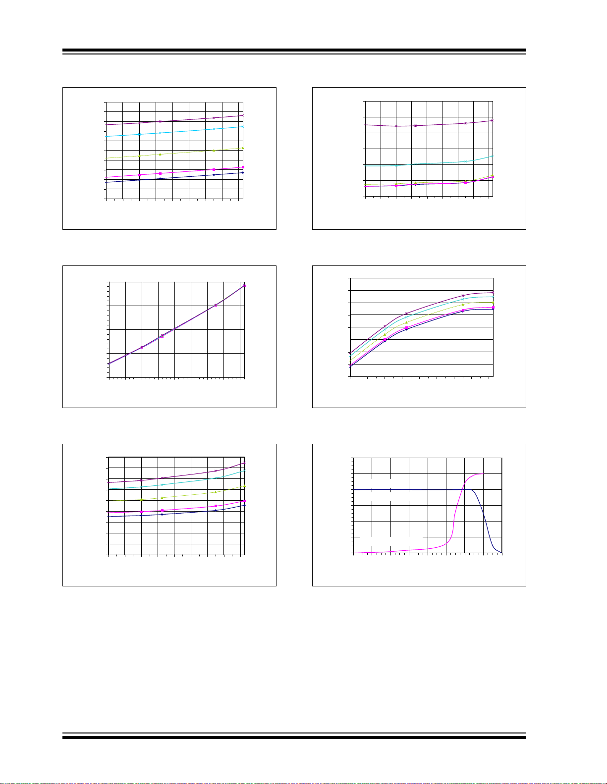
Temperature and V
DD
.
FIGURE 2-21: V
High Threshold vs
IN
Ambient Temperature and V
1.6
1.5
1.4
1.3
1.2
1.1
Low Threshold (V)
IN
1
V
0.9
0.8
-40 -20 0 20 40 60 80 100 120
FIGURE 2-22: V
Ambient Temperature (ºC)
Low Threshold vs
IN
Ambient Temperature and V
DD
DD
.
V
DD
5.5V
5.0V
4.0V
3.0V
2.7V
.
© 2007 Microchip Technology Inc. DS21897B-page 11
MCP4921/4922
V
Note: Unless otherwi se indi cated, TA = +25°C, VDD = 5V , AVSS = 0V, V
2.5
2.25
2
1.75
1.5
1.25
1
Hysteresis (V)
SPI
0.75
_
IN
0.5
V
0.25
0
-40 -20 0 20 40 60 80 100 120
Ambient Temperature (ºC)
FIGURE 2-23: Input Hysteresis vs. Ambient
Temperature and V
175
170
Impedance
165
(kOhm)
160
REF_UNBUFFERED
V
155
-40 -20 0 20 40 60 80 100 120
.
DD
Ambient Temperature (ºC)
V
DD
5.5V
5.0V
4.0V
3.0V
2.7V
5.5V -
2.7V
V
DD
)(V)
SS
Limit (Y-AV
OUT_LOW
V
FIGURE 2-26: V
Temperature and V
(mA)
OUT_HI_SHORTED
I
= 2.048V , G ain = 2, RL = 5 kΩ, CL = 100 pF .
REF
0.0045
0.004
0.0035
0.003
0.0025
0.002
0.0015
-40 -20 0 20 40 60 80 100 120
Ambient Temperature (ºC)
Low Limit vs. Ambient
OUT
.
DD
18
17
16
15
14
13
12
11
10
-40 -20 0 20 40 60 80 100 120
Ambient Temperature (ºC)
V
5.5V
5.0V
4.0V
3.0V
2.7V
V
5.5V
5.0V
4.0V
3.0V
2.7V
DD
DD
FIGURE 2-24: V
Input Impedance vs.
REF
Ambient Temperature and V
0.045
0.04
0.035
-Y)(V)
0.03
DD
0.025
0.02
Limit (V
0.015
0.01
OUT_HI
V
0.005
0
-40 -20 0 20 40 60 80 100 120
Ambient Temperature (ºC)
FIGURE 2-25: V
Temperature and V
High Limit vs. Ambient
OUT
.
DD
DD
FIGURE 2-27: I
.
5.5V
5.0V
4.0
3.0V
2.7V
V
DD
Ambient Temperature and V
6.0
(V)
OUT
V
5.0
4.0
3.0
2.0
1.0
0.0
V
=4.0
REF
Output Shorted to V
Output Shorted to V
0246810121416
FIGURE 2-28: I
High Short vs.
OUT
I
OUT
OUT
DD
SS
(mA)
vs V
DD
.
OUT
. Gain = 1.
DS21897B-page 12 © 2007 Microchip Technology Inc.

MCP4921/4922
Note: Unless otherwi se indicat ed, TA = +25°C, VDD = 5V , AVSS = 0V, V
V
OUT
V
OUT
SCK
LDAC
Time (1 µs/div)
FIGURE 2-29: V
V
OUT
SCK
Rise Time 100%.
OUT
LDAC
FIGURE 2-32: V
V
OUT
SCK
= 2.048V , G ain = 2, RL = 5 kΩ, CL = 100 pF .
REF
Time (1 µs/div)
Rise Time 25% - 75%
OUT
LDAC
Time (1 µs/div)
FIGURE 2-30: V
V
OUT
SCK
LDAC
Time (1 µs/div)
FIGURE 2-31: V
Fall Time.
OUT
Rise Time 50%.
OUT
LDAC
Time (1 µs/div)
FIGURE 2-33: V
Rise Time Exit
OUT
Shutdown.
Ripple Rejection (dB)
Frequency (Hz)
FIGURE 2-34: PSRR vs. Frequency.
© 2007 Microchip Technology Inc. DS21897B-page 13
 Loading...