

Page 1

MCP4802/4812/4822
MCP48X2
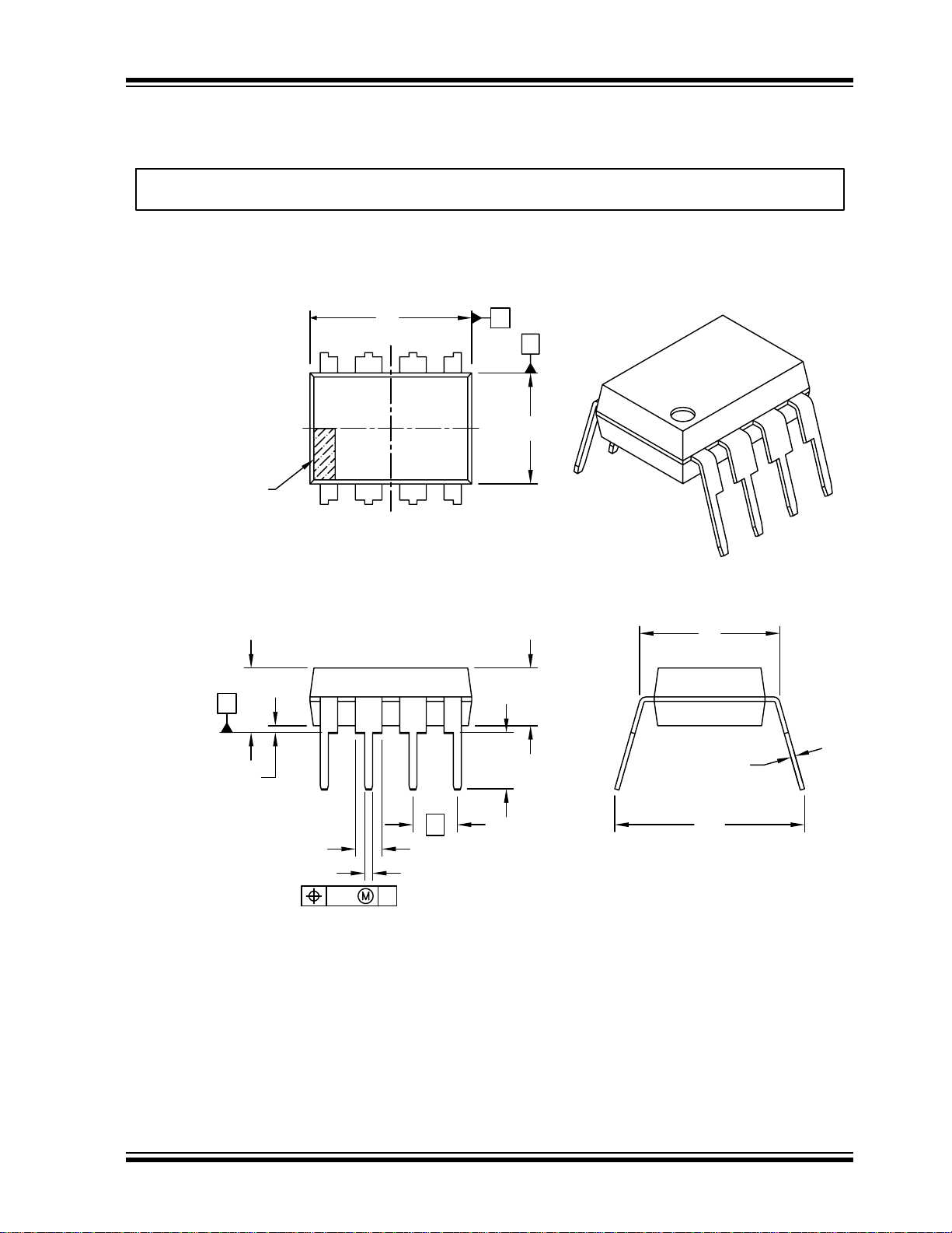
8-Pin PDIP, SOIC, MSOP
1
2
3
4
8
7
6
5
CS
SCK
SDI
V
DD
V
SS
V
OUTA
V
OUTB
LDAC
MCP4802: 8-bit dual DAC
MCP4812: 10-bit dual DAC
MCP4822: 12-bit dual DAC
8/10/12-Bit Dual Voltage Out put Digital-to-Analog Converter
with Internal V
and SPI Interface
REF
Features
• MCP4802: Dual 8-Bit Voltage Output DAC
• MCP4812: Dual 10-Bit Voltage Output DAC
• MCP4822: Dual 12-Bit Voltage Output DAC
• Rail-to-Rail Output
• SPI Interface with 20 MHz Clock Support
• Simultaneous Latching of the Dual DACs
with LDAC pin
• Fast Settling Time of 4.5 µs
• Selectable Unity or 2x Gain Ou tput
• 2.048V Internal Voltage Reference
•50ppm/°C V
• 2.7V to 5.5V Single-Supply Operation
• Extended Temperature Range: -40°C to +125°C
Temperature Coefficient
REF
Applications
• Set Point or Offset Trimming
• Sensor Calibration
• Precision Selectable Voltage Reference
• Portable Instrument ati on (Batte ry-Po w ered )
• Calibration of Optical Communication Devices
DAC
(1)
No. of
Channels
Related Products
P/N
MCP4801 8 1
MCP4811 10 1
MCP4821 12 1
MCP4802 8 2
MCP4812 10 2
MCP4822 12 2
MCP4901 8 1
MCP4911 10 1
MCP4921 12 1
MCP4902 8 2
MCP4912 10 2
MCP4922 12 2
Note 1: The products listed here have similar
Resolution
AC/DC performances.
Voltage
Reference
)
(V
REF
Internal
(2.048V)
External
Description
The MCP4802/4812/4822 devices are dual 8-bit, 10-bit
and 12-bit buffered voltage output Digital-to-Analog
Converters (DACs), respectively. The devices operate
from a single 2.7V to 5.5V supply with SPI compatible
Serial Peripheral Interface.
The devices have a high precision internal voltage
reference (V
full-scale range of the device to be 2.048V or 4.096V by
setting the Gain Selection Option bit (gain of 1 of 2).
Each DAC channel can be operated in Active or
Shutdown mode individually by setting the Configuration
register bits. In Shutdown mode, most of the internal
circuits in the shutdown channel are turned off for power
savings and the output amplifier is configured to present
a known high resistance output load (500 k typical.
The devices include double-buffered registers,
allowing synchronous updates of two DAC outputs
using the LDAC
Power-on Reset (POR) circuit to ensure reliable powerup.
The devices utilize a r esistive string arc hitecture , with
its inherent advantages of low DNL error, low ratio
metric temperature coefficient and fast settling time.
These devices are specified over the extended
temperature range (+125°C).
The devices provide high accuracy and low noise
performance for consumer and industrial applications
where calibration or compensation of signals (such as
temperature, pressure and humidity) are required.
The MCP4802/4812/4822 devices are available in the
PDIP, SOIC and MSOP packages.
= 2.048V). The user can configure the
REF
pin. These devices also incorporate a
Package Types
2010-2015 Microchip Technology Inc. DS20002249B-page 1
Page 2

MCP4802/4812/4822
Op Amps
V
DD
V
SS
CS SDI SCK
Interface Logic
Input
Register A
Register B
Input
DAC
A
Register Register
DAC
B
String
DAC
B
String
DAC
A
Output
Power-on
Reset
V
OUTA
V
OUTB
LDAC
Output
Gain
Logic
Gain
Logic
2.048V
V
REF
Logic
Block Diagram
DS20002249B-page 2 2010-2015 Microchip Technology Inc.
Page 3

MCP4802/4812/4822
1.0 ELECTRICAL CHARACTERISTICS
† Notice: Stresses above those listed under “Maximum
Ratings” may cause permanent damage to the device.
This is a stress rating only and functional operation of
the device at tho se or any oth er conditions ab ove those
Absolute Maximum Ratings †
VDD....................................................................... 6.5V
All inputs and outputs ..........V
– 0.3V to V
SS
DD
+ 0.3V
indicated in the operational listings of this specification
is not implied. Exposure to maximum rating conditions
for extended periods may affect device reliability.
Current at Input Pins .........................................±2 mA
Current at Supply Pins ....................................±50 mA
Current at Output Pins ....................................±25 mA
Storage temperature ..........................-65°C to +150°C
Ambient temp. with power applied.....-55°C to +125°C
ESD protection on all pins 4 kV (HBM), 400V (MM)
Maximum Junction Temperature (T
)................+150°C
J
ELECTRICAL CHARACTERISTICS
Electrical Specifications: Unless otherwise indicated, VDD = 5V, VSS = 0V, V
Output Buffer Gain (G) = 2x, R
Parameters Sym Min Typ Max Units Conditions
Power Requirements
Input Voltage V
Input Current I
Software Shutdown Current I
Power-on Reset Threshold V
DC Accuracy
MCP4802
Resolution n 8 — — Bits
INL Error INL -1 ±0.125 1 LSb
DNL DNL -0.5 ±0.1 +0.5 LSb Note 1
MCP4812
Resolution n 10 — — Bits
INL Error INL -3.5 ± 0.5 3.5 LSb
DNL DNL -0.5 ±0.1 +0.5 LSb Note 1
MCP4822
Resolution n 12 — — Bits
INL Error INL -12 ±2 12 LSb
DNL DNL -0.75 ±0.2 +0.75 LSb Note 1
Offset Error V
Offset Error Temperature
Coefficient
Gain Error g
Gain Error Temperature
Coefficient
Note 1: Guaranteed monotonic by des ign over all codes.
2: This parameter is ensured by design, and not 100% tested.
= 5 k to GND, CL = 100 pF, TA = -40 to +85°C. Typical values are at +25°C.
L
DD
DD
SHDN_SW
POR
OS
V
OS
2.7 — 5.5 V
— 4 15 750 µA All digital inputs are grounded,
—3.3 6 µA
—2.0 — V
-1 ±0.02 1 % of FSR Code = 0x000h
/°C — 0.16 — ppm/°C -45°C to +25°C
— -0.44 — ppm/°C +25°C to +85°C
E
-2 -0.10 2 % of FSR Code = 0xFFFh,
G/°C — -3 — ppm/°C
= 2.048V,
REF
all analog outputs (V
OUT
unloaded. Code = 0x000h
not including offset error
) are
2010-2015 Microchip Technology Inc. DS20002249B-page 3
Page 4

MCP4802/4812/4822
ELECTRICAL CHARACTERISTICS (CONTINUED)
Electrical Specifications: Unless otherwise indicated, VDD = 5V, VSS = 0V, V
Output Buffer Gain (G) = 2x, R
= 5 k to GND, CL = 100 pF, TA = -40 to +85°C. Typical values are at +25°C.
L
Parameters Sym Min Typ Max Units Conditions
Internal Voltage Reference (V
Internal Reference V o lt a ge V
Temperature Coefficient
(Note 2)
)
REF
2.008 2.048 2.088 V V
/°C — 125 325 ppm/°C -40°C to 0°C
V
REF
REF
— 0.25 0.65 LSb/°C -40°C to 0°C
— 45 160 ppm/°C 0°C to +85°C
— 0.09 0.32 LSb/°C 0°C to +85°C
Output Noise (V
Noise) E
REF
NREF
—290 —µV
(0.1-
10 Hz)
Output Noise Density e
NREF
—1.2 —µV/Hz Code = 0xFFFh, G = 1x
(1 kHz)
e
NREF
—1.0 —µV/Hz Code = 0xFFFh, G = 1x
(10 kHz)
1/f Corner Frequency f
CORNER
—400 — Hz
Output Amplifier
Output Swing V
OUT
— 0.01 to
– 0.04
V
DD
— V Accuracy is better than 1LSb for
Phase Margin PM — 66 — Degree
Slew Rate SR — 0.55 — V/µs
Short Circuit Current I
Settling Time t
SETTLING
SC
—1524mA
— 4.5 — µs Within 1/2 LSb of final value from
Dynamic Performance (Note 2)
DAC-to-DAC Crosstalk — <10 — nV-s
Major Code Transition Glitch — 45 — nV-s 1 LSb change around major carry
Digital Feedthrough — <10 — nV-s
Analog Crosstalk — <10 — nV-s
Note 1: Guaranteed monotonic by des ign over all codes.
2: This parameter is ensured by design, and not 100% tested.
= 2.048V,
REF
(°)
when G = 1x and
OUTA
Code = 0xFFFh
Code = 0xFFFh, G = 1x
p-p
V
= 10 mV to (VDD–40 mV)
OUT
= 400 pF, RL =
C
L
1/4 to 3/4 full-scale range
(0111...1111 to
1000...0000)
DS20002249B-page 4 2010-2015 Microchip Technology Inc.
Page 5

MCP4802/4812/4822
ELECTRICAL CHARACTERISTIC WITH EXTE NDED TEMPERATURE
Electrical Specifications: Unless otherwise indicated, V
= 5 k to GND, CL = 100 pF. Typical values are at +125°C by characterization or simulation.
R
L
Parameters Sym Min Typ Max Units Conditions
Power Requirements
Input Voltage V
Input Current
DD
I
DD
2.7 — 5.5 V
Input Curren
Software Shutdown Curren t I
Power-On Reset threshold V
SHDN_SW
POR
DC Accuracy
MCP4802
Resolution n 8 — — Bits
INL Error INL — ±0.25 — LSb
DNL DNL — ±0.2 — LSb Note 1
MCP4812
Resolution n 10 — — Bits
INL Error INL — ±1 — LSb
DNL DNL — ±0.2 — LSb Note 1
MCP4822
Resolution n 12 — — Bits
INL Error INL — ±4 — LSb
DNL DNL — ±0.25 — LSb Note 1
Offset Error V
Offset Error Temperature
OS
VOS/°C — -5 — ppm/°C +25°C to +125°C
Coefficient
Gain Error g
Gain Error Temperature
E
G/°C — -3 — ppm/°C
Coefficient
Internal Voltage Reference (V
Internal Reference V o lt a ge V
Temperature Coefficient
)
REF
REF
V
/°C — 125 — ppm/°C -40°C to 0°C
REF
(Note 2)
Output Noise (V
Noise) E
REF
NREF
(0.1 – 10 Hz)
Output Noise Density e
NREF
(1 kHz)
e
NREF
(10 kHz)
1/f Corner Frequency f
CORNER
Note 1: Guaranteed monotonic by des ign over all codes.
2: This parameter is ensured by design, and not 100% tested.
DD
= 5V, V
SS
= 0V, V
= 2.048V, Output Buffer Gain (G) = 2x,
REF
— 440 — µA All digital inputs are grounded,
all analog outputs (V
unloaded. Code = 0x000h.
—5—µA
—1.85— V
— ±0.02 — % of FSR Code = 0x000h
— -0.10 — % of FSR Code = 0xFFFh,
not including offset error
— 2.048 — V V
when G = 1x and
OUTA
Code = 0xFFFh
— 0.25 — LSb/°C -40°C to 0°C
— 45 — ppm/°C 0°C to +85°C
— 0.09 — LSb/°C 0°C to +85°C
— 290 — µV
—1.2—µV/
—1.0—µV/
Code = 0xFFFh, G = 1x
p-p
Hz Code = 0xFFFh, G = 1x
Hz Code = 0xFFFh, G = 1x
— 400 — Hz
OUT
) are
2010-2015 Microchip Technology Inc. DS20002249B-page 5
Page 6

MCP4802/4812/4822
ELECTRICAL CHARACTERISTIC WITH EXTE NDED TEMPERATURE (CONTINUED)
Electrical Specifications: Unless otherwise indicated, V
= 5 k to GND, CL = 100 pF. Typical values are at +125°C by characterization or simulation.
R
L
Parameters Sym Min Typ Max Units Conditions
Output Amplifier
Output Swing V
OUT
Phase Margin PM — 66 — Degree (°) C
Slew Rate SR — 0.55 — V/µs
Short Circuit Current I
Settling Time t
SC
SETTLING
Dynamic Performance (Note 2)
DAC-to-DAC Crosstalk — <10 — nV-s
Major Code Transition
Glitch
Digital Feedthrough — <10 — nV-s
Analog Crosstalk — <10 — nV-s
Note 1: Guaranteed monotonic by des ign over all codes.
2: This parameter is ensured by design, and not 100% tested.
= 5V, V
DD
— 0.01 to
V
DD
SS
– 0.04
= 0V, V
= 2.048V, Output Buffer Gain (G) = 2x,
REF
— V Accuracy is better than 1 LSb
for
V
= 10 mV to (VDD –
OUT
40 mV)
= 400 pF, RL =
L
—17—mA
— 4.5 — µs Within 1/2 LSb of final value
from 1/4 to 3/4 full-scale ra nge
— 45 — nV-s 1 LSb change around major
carry (0111...1111 to
1000...0000)
AC CHARACTERISTICS (SPI TIMING SPECIFICATIONS)
Electrical Specifications: Unless otherwise indicated, V
Typical values are at +25°C.
Parameters Sym Min Typ Max Units Conditions
Schmitt Trigger High-Level
V
0.7 V
IH
DD
Input Voltage
(All digital input pins)
Schmitt Trigger Low-Level
V
IL
——0.2VDDV
Input Voltage
(All digital input pins)
Hysteresis of Schmitt Trigger
V
HYS
—0.05VDD—V
Inputs
Input Leakage Current I
LEAKAGE
Digital Pin Capacitance
(All inputs/outputs)
C
Clock Frequency F
Clock High Time t
Clock Low Time t
Fall to First Rising CLK
CS
t
CIN,
OUT
CLK
HI
LO
CSSR
-1 — 1 ALDAC = CS = SDI = SCK =
—10—pFV
——20MHzT
15 — — ns Note 1
15 — — ns Note 1
40 — — ns Applies only when CS falls with
Edge
Data Input Setup Time t
Data Input Hold Time t
SCK Rise to CS
Rise Hold
SU
HD
t
CHS
15 — — ns Note 1
10 — — ns Note 1
15 — — ns Note 1
Time
Note 1: This parameter is ensured by design and not 100% tested.
= 2.7V – 5.5V, TA= -40 to +125°C.
DD
——V
V
or V
DD
SS
= 5.0V, TA = +25°C,
DD
= 1 MHz (Note 1)
f
CLK
= +25°C (Note 1)
A
CLK high. (Note 1)
DS20002249B-page 6 2010-2015 Microchip Technology Inc.
Page 7

MCP4802/4812/4822
CS
SCK
SDI
LDAC
t
CSSR
t
HD
t
SU
t
LO
t
CSH
t
CHS
LSb in
MSb in
t
IDLE
Mode 1,1
Mode 0,0
t
HI
t
LD
t
LS
AC CHARACTERISTICS (SPI TIMING SPECIFICATIONS)
Electrical Specifications: Unless otherwise indicated, V
Typical values are at +25°C.
Parameters Sym Min Typ Max Units Conditions
CS High Time t
LDAC Pulse Width t
Setup Time t
LDAC
SCK Idle Time before CS Fal l t
CSH
LD
LS
IDLE
15 — — ns Note 1
100 — — ns Note 1
40 — — ns Note 1
40 — — ns Note 1
Note 1: This parameter is ensured by design and not 100% tested.
= 2.7V – 5.5V, TA= -40 to +125°C.
DD
FIGURE 1-1: SPI Input Timing Data.
TEMPERATURE CHARACTERISTICS
Electrical Specifications: Unless otherwise indicated, VDD= +2.7V to +5.5V, VSS= GND.
Parameters Sym Min Typ Max Units Conditions
Temperature Ranges
Specified Temperature Range T
Operating Temperature Range T
Storage Temperature Range T
Thermal Package Resistances
Thermal Resistance, 8L-MSOP
Thermal Resistance, 8L-PDIP
Thermal Resistance, 8L-SOIC
Note 1: The MCP4802/4812/4822 devices operate over this extended temperature range, but with reduced
performance. Operation in this range must not cause T
of +150°C.
JA
JA
JA
A
A
A
-40 — +125 °C
-40 — +125 °C Note 1
-65 — +150 °C
—211—°C/W
—90—°C/W
—150—°C/W
to exceed the maximum junction temperature
J
2010-2015 Microchip Technology Inc. DS20002249B-page 7
Page 8

MCP4802/4812/4822
NOTES:
DS20002249B-page 8 2010-2015 Microchip Technology Inc.
Page 9

MCP4802/4812/4822
-0.3
-0.2
-0.1
0
0.1
0.2
0.3
0 1024 2048 3072 4096
Code (Decimal)
DNL (L SB)
-0.2
-0.1
0
0.1
0.2
0 1024 2048 3072 4096
Code (Decimal)
DNL (LSB)
125C 85C 25C
0.075
0.0752
0.0754
0.0756
0.0758
0.076
0.0762
0.0764
0.0766
-40-200 20406080100120
Ambient Temperature (ºC)
Absolute DNL (LSB)
-5
-4
-3
-2
-1
0
1
2
3
4
5
0 1024 2048 3072 4096
Code (Decimal)
INL (LSB)
125C 85 25
Ambient Temperat ure
0
0.5
1
1.5
2
2.5
-40 -20 0 20 40 60 80 100 120
Ambient Temperature (ºC)
Absolute IN L (LS B)
-6
-4
-2
0
2
0 1024 2048 3072 4096
Code (Decimal )
INL (LSB)
2.0 TYPICAL PERFORMANCE CURVES
Note: The graphs and table s prov ided following this note are a st a tis tic al s umm ary based on a limited number of
samples and are provided for informational purposes only. The performance characteristics listed herein
are not tested or guaranteed. In some graphs or tables, the data presented may be outside the specified
operating range (e.g., outside specified power supply range) and therefore outside the warranted range.
Note: Unless otherwise in dic ate d, TA = +25°C, VDD = 5V, VSS = 0V, V
FIGURE 2-1: DNL vs. Code (MCP4822).
FIGURE 2-4: INL vs. Code and
Temperature (MCP4822).
= 2.048V, Gain = 2x, RL = 5 k, CL = 100 pF.
REF
FIGURE 2-2: DNL vs. Code and Temperature (MCP4822).
FIGURE 2-3: Absolute DNL vs. Temperature (MCP4822).
2010-2015 Microchip Technology Inc. DS20002249B-page 9
FIGURE 2-5: Absolute INL vs. Temperature (MCP4822).
FIGURE 2-6: INL vs. Code (MCP4822 ).
Note: Single device graph for illustration of 64
code effect.
Page 10

MCP4802/4812/4822
-0.3
-0.2
-0.1
0
0.1
0.2
0.3
0 128 256 384 512 640 768 896 1024
Code
DNL (LSB)
- 40oC
+25oC to +125oC
-3
-2.5
-2
-1.5
-1
-0.5
0
0.5
1
1.5
0 128 256 384 512 640 768 896 1024
INL (LSB)
25oC
85oC
125oC
- 40oC
-0.15
-0.1
-0.05
0
0.05
0.1
0.15
0 32 64 96 128 160 192 224 256
Code
DNL (LSB)
34
Temperature: - 40oC to +125
o
-0.3
-0.2
-0.1
0
0.1
0.2
0.3
0.4
0.5
0.6
0 326496128160192224256
Code
INL (LSB)
-
o
C
25oC
85oC
125oC
2.040
2.041
2.042
2.043
2.044
2.045
2.046
2.047
2.048
2.049
2.050
-40 -20 0 20 40 60 80 100 120
Ambient Temperature (°C)
Full Scale V
OUT
(V)
VDD: 4V
VDD: 3V
VDD: 2.7V
4.076
4.080
4.084
4.088
4.092
4.096
4.100
-40 -20 0 20 40 60 80 100 120
Ambient Temperature (°C)
Full Scal e V
OUT
(V)
VDD: 5.5V
VDD: 5V
Note: Unless otherwise in dic ate d, TA = +25°C, VDD = 5V, VSS = 0V, V
FIGURE 2-7: DNL vs. Code and Temperature (MCP4812).
FIGURE 2-10: INL vs. Code and Temperature (MCP4802).
= 2.048V, Gain = 2x, RL = 5 k, CL = 100 pF.
REF
40
Code
FIGURE 2-8: INL vs. Code and
FIGURE 2-11: Full-Scale V
Ambient Temperature and V
DD
vs.
OUTA
. Gain = 1x.
Temperature (MCP4812).
C
FIGURE 2-9: DNL vs. Code and Temperature (MCP4802).
DS20002249B-page 10 2010-2015 Microchip Technology Inc.
FIGURE 2-12: Full-Scale V
Ambient Temperature and V
DD
vs.
OUTA
. Gain = 2x.
Page 11

MCP4802/4812/4822
1.E-07
1.E-06
1.E-05
1.E-04
1E-1 1E+0 1E+1 1E+2 1E+3 1E+4 1E+5
Frequency (Hz)
Output Noise Voltage Densit y
(µV/
Hz)
1 10 100 1k 10k 100k
100
10
1
0.1
1.E-05
1.E-04
1.E-03
1.E-02
1E+2 1E+3 1E+4 1E+5 1E+6
Bandwidth (Hz)
Output Noise Voltage (mV)
100 1k 10k 100k 1M
Eni (in V
RMS
)
10.0
1.00
0.10
0.01
Eni (in V
P-P
)
Maximum Measurement Time = 10s
180
200
220
240
260
280
300
320
340
-40-200 20406080100120
Ambien t Te mp e r at ure (°C)
I
DD
(µA)
V
DD
5.5V
4.0V
5.0V
3.0V
2.7V
0
5
10
15
20
25
380
385
390
395
400
405
410
415
420
425
430
435
440
IDD (µA)
Occurrence
0
2
4
6
8
10
12
14
16
18
20
22
385
390
395
400
405
410
415
420
425
430
435
IDD (µA)
Occurrence
Note: Unless otherwise in dic ate d, TA = +25°C, VDD = 5V, VSS = 0V, V
0.1
FIGURE 2-13: Output Noise Voltage
Density (V
Noise Density) vs. Frequency.
REF
FIGURE 2-16: IDD Histogram (VDD = 2.7V).
Gain = 1x.
= 2.048V, Gain = 2x, RL = 5 k, CL = 100 pF.
REF
FIGURE 2-14: Output Noise Voltage
(V
Noise Voltage) vs. Bandwidth. Gain = 1x.
REF
FIGURE 2-15:
2010-2015 Microchip Technology Inc. DS20002249B-page 11
IDD vs. Temperature and VDD.
FIGURE 2-17: I
Histogram (VDD = 5.0V).
DD
Page 12

MCP4802/4812/4822
1
1.5
2
2.5
3
3.5
4
-40-20 0 20406080100120
Ambient Temperature (ºC)
I
SHDN_SW
(µA)
V
DD
5.5V
4.0V
5.0V
3.0V
2.7V
-0.03
-0.01
0.01
0.03
0.05
0.07
0.09
0.11
-40 -20 0 20 40 60 80 100 120
Ambien t Te m p er at u re ( ºC)
Offset Error (%)
V
DD
5.5V
5.0V
3.0V
2.7V
-0.5
-0.45
-0.4
-0.35
-0.3
-0.25
-0.2
-0.15
-0.1
-0.05
-40 -20 0 20 40 60 80 100 120
Ambient Te m pe r at ure (ºC)
Gain Error (%)
V
DD
5.5V
4.0V
5.0V
3.0V
2.7V
1
1.5
2
2.5
3
3.5
4
-40-200 20406080100120
Ambient Temperature (ºC)
V
IN
Hi Threshold (V)
V
DD
5.5V
4.0V
5.0V
3.0V
2.7V
0.8
0.9
1
1.1
1.2
1.3
1.4
1.5
1.6
-40 -20 0 20 40 60 80 100 120
Ambient Temperature (ºC)
V
IN
Low Threshold (V)
V
DD
5.5V
4.0V
5.0V
3.0V
2.7V
Note: Unless otherwise in dic ate d, TA = +25°C, VDD = 5V, VSS = 0V, V
FIGURE 2-18: Software Shutdown Current
vs. Temperature and V
DD
.
FIGURE 2-21: V
Temperature and V
= 2.048V, Gain = 2x, RL = 5 k, CL = 100 pF.
REF
High Threshold vs.
IN
.
DD
FIGURE 2-19: Offset Error vs. Temperature
DD
.
and V
FIGURE 2-20: Gain Error vs. Temperature
and V
DS20002249B-page 12 2010-2015 Microchip Technology Inc.
DD
.
4.0V
FIGURE 2-22: V
Temperature and V
Low Threshold vs.
IN
.
DD
Page 13

MCP4802/4812/4822
0
0.25
0.5
0.75
1
1.25
1.5
1.75
2
2.25
2.5
-40-200 20406080100120
Ambient Temperature (ºC)
V
IN
_
SPI
Hysteresis (V)
V
DD
5.5V
4.0V
5.0V
3.0V
2.7V
0.015
0.017
0.019
0.021
0.023
0.025
0.027
0.029
0.031
0.033
0.035
-40-200 20406080100120
Ambient Temperature (ºC)
V
OUT_HI
Limi t ( V
DD
-Y)(V)
V
DD
3.0V
2.7V
0.0010
0.0012
0.0014
0.0016
0.0018
0.0020
0.0022
0.0024
0.0026
0.0028
-40-200 20406080100120
Ambient Temperature (ºC)
V
OUT_LOW
Limit (Y-AV
SS
)(V)
V
DD
5.5V
4.0V
5.0V
3.0V
2.7V
10
11
12
13
14
15
16
-40 -20 0 20 40 60 80 100 120
Ambient Temperature (ºC)
I
OUT_HI_SHORTED
(mA)
V
DD
4
3
2
0.0
1.0
2.0
3.0
4.0
5.0
6.0
0246810121416
I
OUT
(mA)
V
OUT
(V)
V
REF
= 4.096V
Output Shorted to V
SS
Output Shorted to V
DD
Note: Unless otherwise in dic ate d, TA = +25°C, VDD = 5V, VSS = 0V, V
FIGURE 2-23: Input Hysteresis vs.
Temperature and V
DD
.
4.0V
FIGURE 2-26: I
Temperature and V
= 2.048V, Gain = 2x, RL = 5 k, CL = 100 pF.
REF
High Short vs.
OUT
.
DD
5.5V
5.0V
.0V
.0V
.7V
FIGURE 2-24: V
vs.Temperature and V
FIGURE 2-25: V
Temperature and V
2010-2015 Microchip Technology Inc. DS20002249B-page 13
DD
OUT
DD
OUT
.
.
High Limit
Low Limit vs.
FIGURE 2-27: I
OUT
vs. V
. Gain = 2x.
OUT
Page 14

MCP4802/4812/4822
V
OUT
SCK
LDAC
Time (1 µs/div)
V
OUT
SCK
LDAC
Time (1 µs/div)
V
OUT
SCK
LDAC
Time (1 µs/div)
Time (1 µs/div)
V
OUT
LDAC
Time (1 µs/div)
V
OUT
SCK
LDAC
Ripple Rejection (dB)
Frequency (Hz)
Note: Unless otherwise in dic ate d, TA = +25°C, VDD = 5V, VSS = 0V, V
FIGURE 2-28: V
Rise Time.
OUT
FIGURE 2-31: V
= 2.048V, Gain = 2x, RL = 5 k, CL = 100 pF.
REF
Rise Time.
OUT
FIGURE 2-29: V
Fall Time.
OUT
FIGURE 2-32: V
Rise Time Exit
OUT
Shutdown.
FIGURE 2-30: V
DS20002249B-page 14 2010-2015 Microchip Technology Inc.
Rise Time.
OUT
FIGURE 2-33: PSRR vs. Frequency.
Page 15

MCP4802/4812/4822
3.0 PIN DESCRIPTIONS
The descriptions of the pins are listed in Table 3-1.
TABLE 3-1: PIN FUNCTION TABLE FOR MCP4802/4812/4822
MCP4802/4812/4822
MSOP, PDIP, SOIC
1V
2CSChip Select Input
3 SCK Serial Clock Input
4 SDI Serial Data Input
5LDAC
6V
7V
8V
Symbol Description
DD
Supply Voltage Input (2.7V to 5.5V)
Synchronization Input. This pin is used to transfer DAC settings
(Input Registers) to the output registers (V
OUTB
SS
OUTA
DACB Output
Ground reference point for all circuitry on the device
DACA Output
OUT
)
3.1 Supply Volt age Pins (V
DD, VSS
)
VDD is the po siti ve sup ply v oltage input pin. The i nput
supply voltage is relative to V
2.7V to 5.5V. The power supply at the V
and can range from
SS
pin should
DD
be as clean as possible for a good DAC performance.
It is recommended to use an appropriate bypass
capacitor of about 0.1 µF (ceramic) to ground. An
additional 10 µF capacitor (tantalum) in parallel is also
recommended to further attenuate high-frequency
noise present in application boards.
is the analog ground pin and the current return path
V
SS
of the device. The user must connect the V
pin to a
SS
ground plane through a low-impedance connection. If
an analog ground path is available in the application
Printed Circuit Board (PCB), it is highly recommended
that the VSS pin be tied to the analog ground path or
isolated within an analog ground plane of the circuit
board.
3.2 Chip Select (CS)
CS is the Chip Select input pin, which requires an
active-low to enable serial clock and data functions.
3.3 Serial Clock Input (SCK)
3.4 Serial Data Input (SDI)
SDI is the SPI compatible serial data input pin.
3.5 Latch DAC Input (LDAC)
LDAC (latch DAC sync hro ni z at i on i npu t ) pi n is us ed to
transfer the input latch registers to their corresponding
DAC registers (output latches, V
low, both V
OUTA
and V
are updated at the same
OUTB
time with t heir input regi ster c onten ts. This pin can be
tied to low (VSS) if the V
rising edge of the CS
OUT
pin. This pin can be driven by an
external control device such as an MCU I/O pin.
3.6 Analog Outputs (V
V
is the DAC A output pin, and V
OUTA
B output pin. Each output has its own output amplifier.
The full-scale range of the DAC output is from
to G* V
V
SS
(1x or 2x). The DAC analog output cannot go higher
than the supply voltag e (V
, where G is the gain selection option
REF
DD
). When this pin is
OUT
update is desired at the
OUTA
, V
OUTB
)
OUTB
is the DAC
).
SCK is the SPI compatible serial clock input pin.
2010-2015 Microchip Technology Inc. DS20002249B-page 15
Page 16

MCP4802/4812/4822
NOTES:
DS20002249B-page 16 2010-2015 Microchip Technology Inc.
Page 17

MCP4802/4812/4822
V
OUT
2.048V D
n
2
n
----------------------------------- G=
Where:
2.048V = Internal voltage reference
D
n
= DAC input code
G = Gain selection
=2 for <GA
> bit = 0
=1 for <GA> bit = 1
n = DAC Resolution
=8 for MCP4802
= 10 for MCP4812
= 12 for MCP4822
111
110
101
100
011
010
001
000
Digital
Input
Code
Actual
Transfer
Function
INL < 0
Ideal Transfer
Function
INL < 0
DAC Output
4.0 GENERAL OVERVIEW
The MCP4802, MCP4812 and MCP4822 are dual
voltage output 8-bit, 10-bit and 12-bit DAC devices,
respectively. These devices include rail-to-rail output
amplifiers, internal voltage reference, shutdown and
reset-management circuitry. The devices use an SPI
serial communication interface and operate with a single supply voltage from 2.7V to 5.5V.
The DAC input coding of these devices is straight
binary. Equation 4-1 shows the DAC analog output
voltage calculation.
EQUATION 4-1: ANALOG OUTPUT
VOLTAGE (V
OUT
)
1 LSb is the ideal voltage difference between two
successive codes. Table 4-1 illustrates the LSb
calculation of each device.
TABLE 4-1: LSb OF EACH DEVICE
Device
MCP4802
(n = 8)
MCP4812
(n = 10)
MCP4822
(n = 12)
Gain
Selection
1x 2.048V/256 = 8 mV
2x 4.096V/256 = 16 mV
1x 2.048V/1024 = 2 mV
2x 4.096V/1024 = 4 mV
1x 2.048V/4096 = 0.5 mV
2x 4.096V/4096 = 1 mV
LSb Size
4.0.1 INL ACCURACY
Integral Non-Linearity (INL) error for these devices is
the maximum devi ation be tween an actua l code tra nsition point and its corresponding ideal transition point
once offset and gain errors have been removed. The
two end points method (from 0x000 to 0xFFF) is used
for the calculation. Figure 4-1 shows the details.
A positive INL error represents transition(s) later than
ideal. A negative INL error represents transition(s)
earlier than ideal.
The ideal output range of each device is:
• MCP4802 (n = 8)
(a) 0.0V to 255/256 * 2.048V when gain setting = 1x.
(b) 0.0V to 255/256 * 4.096V when gain setting = 2x.
• MCP4812 (n = 10)
(a) 0.0V to 1023/1024 * 2.048V when g ain setting= 1x.
(b) 0.0V to 1023/1024 * 4.096 V when gain setting = 2x.
• MCP4822 (n = 12)
(a) 0.0V to 4095/4096 * 2.048V when g ain setting= 1x.
(b) 0.0V to 4095/4096 * 4.096V when g ain setting= 2x.
Note:
2010-2015 Microchip Technology Inc. DS20002249B-page 17
See the output swing voltage specification in
Section 1.0 “Electrical Characteristics”
.
FIGURE 4-1: Example for INL Error.
Page 18

MCP4802/4812/4822
111
110
101
100
011
010
001
000
Digital
Input
Code
Actual
Transfer
Function
Ideal Transfer
Function
Narrow Code, <1 LSb
DAC Output
Wide Code , >1 LSb
4.0.2 DNL ACCURACY
A Differential Non-Li ne arity (DNL) error is the measure
of variations in code widths from the ideal code width.
A DNL error of zero indicate s that every co de is exa ctly
1 LSb wide.
FIGURE 4-2: Example for DNL Error.
4.0.3 OFFSET ERROR
An offset erro r is the devi ation from z ero vol tag e outp ut
when the digital input code is zero.
4.0.4 GAIN ERROR
A gain error is the deviation from the ideal output,
– 1 LSb, excluding the effects of offset error.
V
REF
4.1 Circuit Descriptions
4.1.1 OUTPUT AMPLIFIERS
The DAC’s outputs are buffered with a low-power,
precision CMOS amplifier. This amplifier provides low
offset volt ag e an d l ow no is e. T he o utp ut s tage enables
the device to operate with output voltages close to the
power supply rails. Refer to Section 1.0 “Electrical
Characteristics” for the analog output voltage range
and load conditions.
In addition to resistive load-driving capability, the
amplifier will also drive high capacitive loads without
oscillation. The ampl ifier’s strong ou tputs allow V
be used as a programmable voltage reference in a
system.
4.1.1.1 Programmable Gain Block
The rail-to-rail output amplifier has two configurable
gain options: a gain of 1x (<GA
> = 0). The default value for this bit is a gain
(<GA
of 2 (<GA
output of 0.000V to 4.096V due to the internal
reference (V
> = 0). This results in an ideal full-scale
= 2.048V).
REF
> = 1) or a gain of 2x
4.1.2 VOLTAGE REFERENCE
The MCP4802/4812/4822 devices utilize internal
2.048V voltage refere nce. The volt a ge referen ce has a
low temperature coefficient and low noise
characteristics. Refer to Section 1.0 “Electrical Char-
acteristics” for the voltage reference specifications.
OUT
to
DS20002249B-page 18 2010-2015 Microchip Technology Inc.
Page 19

MCP4802/4812/4822
Transients above the curve
will cause a reset
Transients below the curve
will NOT cause a reset
5V
Time
Supply Voltages
Transient Duration
V
POR
VDD - V
POR
TA = +25°C
Transient Duration (µs)
10
8
6
4
2
0
12345
V
DD
- V
POR
(V)
500 k
Power-Down
Control Circuit
Resistive
Load
V
OUT
Op
Amp
Resistive String DAC
4.1.3 POWER-ON RESET CIRCUIT
The internal Power-on Res et (POR) circuit moni tors the
power supply voltage (V
operation. The circuit also ensures that the DAC
powers up with high output impedance (<SHDN> = 0,
typically 500 k. The devices will continue to have a
high-impedance output until a valid write command is
received and the LDAC
threshold.
If the power supply voltage is less than the POR
threshold (V
= 2.0V, typical), the DACs will be held
POR
in their Reset state. The DACs will remain in that state
until VDD > V
and a subsequent write command is
POR
received.
Figure 4-3 shows a typical power supply transient
pulse and the duration required to cause a reset to
occur, as well as the relationship between the duration
and trip voltage. A 0.1 µF decoupling capacitor,
mounted as close as possible to the V
provide additional transient immunity.
) during the device
DD
pin meets the input low
pin, can
DD
4.1.4 SHUTDOWN MODE
The user can shut down each DAC channel selectively
using a software command (<SHDN
Shutdown mode, most of the internal circuits in the
channel that was shut down are turned off for power
savings. The internal reference is not affected by the
shutdown command. The serial interface also remains
active, thus allowing a write command to bring the
device out of the Shutdown mode. There will be no
analog output at the channel that was shut down and
the V
pin is internally switc he d to a known resistive
OUT
load (500 k typical. Figure 4-4 shows the analog
output stage during the Shutdown mode.
The device will remain in Shutdown mode until the
<SHDN
> bit = 1 is latched into the device. When a
DAC channel is changed from Shutdown to Active
mode, the output settling time takes < 10 µs, but
greater than the standard active mode settling time
(4.5 µs).
> = 0). During
FIGURE 4-4: Output Stage for Shutdown Mode.
FIGURE 4-3: Typical Transient Respon se .
2010-2015 Microchip Technology Inc. DS20002249B-page 19
Page 20

MCP4802/4812/4822
NOTES:
DS20002249B-page 20 2010-2015 Microchip Technology Inc.
Page 21

MCP4802/4812/4822
5.0 SERIAL INTERFACE
5.1 Overview
The MCP4802/4812/4822 devices are designed to
interface directly with the Serial Peripheral Interface
(SPI) port, available on many microcontrollers, and
supports Mode 0,0 and Mod e 1,1. Comma nds and da ta
are sent to the device via the SDI pin, with data being
clocked-in on the rising edge of SCK. The
communications are unidirectional and, thus, data
cannot be read out of the MCP4802/4812/4822
devices. The CS
of a write command. The write command consists of
16 bits and is used to configure the DAC’s control and
data latches. Register 5-1 to Register 5-3 detail the
input register that is used to configure and load the
and DACB registers for each device. Figure 5-1
DAC
A
to Figure5-3 show the write command for eac h devic e.
Refer to Figure 1-1 and SPI Timing Specifications
Table for detailed input and outpu t timing sp ecification s
for both Mode 0,0 and Mode 1,1 operation.
pin must be held low for the duration
5.2 Write Command
The write command is initiated by driving the CS pin
low, followed by clocking the four Configuration bits and
the 12 data bits into the SDI pin on the rising edge of
SCK. The CS
latched into the selected DAC’s input registers.
The MCP4802/4812/4822 devices utilize a doublebuffered latch structure to allow both DAC
DAC
’s outputs to b e s ynchro ni zed with the LDAC pi n,
B
if desired.
By bringing down the LDAC
tents stored in the DA C’s input reg isters are transferre d
into the DAC’s output registers (V
and V
OUTB
All writes to the MCP4802/4812/4822 devices are
16-bit words. Any clocks af ter the fi rst 16
ignored. The Most Significant four bits are
Configuration bits. The remaining 12 bits are data bits.
No data can be transferred into the device with CS
high. The data transfe r will on ly occur if 16 c locks have
been transferred into the device. If the rising edge of
occurs prior, shifting of data into the input registers
CS
will be aborted.
pin is then ra is ed, ca us ing th e data to be
A
pin to a low s tate, the con-
), and both V
are updated at the same time.
OUT
th
clock will be
’s and
OUTA
2010-2015 Microchip Technology Inc. DS20002249B-page 21
Page 22

MCP4802/4812/4822
W-x W-x W-x W-0 W-x W-x W-x W-x W-x W-x W-x W-x W-x W-x W-x W-x
A
/B — GA SHDN D11 D10 D9 D8 D7 D6 D5 D4 D3 D2 D1 D0
bit 15 bit 0
W-x W-x W-x W-0 W-x W-x W-x W-x W-x W-x W-x W-x W-x W-x W-x W-x
A/B — GA SHDN D9 D8 D7 D6 D5 D4 D3 D2 D1 D0 x x
bit 15 bit 0
W-x W-x W-x W-0 W-x W-x W-x W-x W-x W-x W-x W-x W-x W-x W-x W-x
A
/B — GA SHDN D7 D6 D5 D4 D3 D2 D1 D0 x xxx
bit 15 bit 0
Legend
R = Readable bit W = Writable bit U = Unimplemented bit, read as ‘0’
-n = Value at POR 1 = bit is set 0 = bit is cleared x = bit is unknown
REGISTER 5-1: WRITE COMMAND REGISTER FOR MCP4822 (12-BIT DAC)
REGISTER 5-2: WRITE COMMAND REGISTER FOR MCP4812 (10-BIT DAC)
REGISTER 5-3: WRITE COMMAND REGISTER FOR MCP4802 (8-BIT DAC)
Where:
bit 15 A/B: DACA or DACB Selection bit
1 = Write to DAC
0 = Write to DAC
bit 14 — Don’t Care
bit 13 GA
: Output Gain Selection bit
1 =1x (V
0 =2x (V
OUT
OUT
bit 12 SHDN: Outp ut Shutdown Control bit
1 = Active mode operation. VOUT is available.
0 = Shutdown the selected DAC cha nnel. Analog outp ut is not availab le at the channel t hat was shut down.
V
pin is connected to 500ktypical)
OUT
bit 11-0 D11:D0: DAC Input Data bits. Bit x is ignored.
B
A
= V
REF
= 2 * V
* D/4096)
* D/4096), where internal VREF = 2.048V.
REF
DS20002249B-page 22 2010-2015 Microchip Technology Inc.
Page 23

MCP4802/4812/4822
SDI
SCK
CS
0
21
A
/B — GA SHDN D11
D10
config bits 12 data bits
LDAC
3 4
D9
5
6
7
D8
D7
D6
8 9 10 12
D5
D4
D3
D2
D1 D0
11
13
14 15
V
OUT
(Mode 1,1)
(Mode 0,0)
SDI
SCK
CS
0
21
A
/B — GA SHDN D9
D8
config bits 12 data bits
LDAC
3 4
D7
5 6
7
D6
D5
D4
8
9 10 12
D3
D2
D1
D0
X X
11
13
14 15
V
OUT
(Mode 1,1)
(Mode 0,0)
Note: X = “don’t care” bits.
SDI
SCK
CS
0
21
A
/B — GA SHDN
config bits 12 data bits
LDAC
3 4
5
6
7
X
D7
D6
8 9 10 12
D5
D4
D3
D2
D1
D0
11
13
14 15
V
OUT
(Mode 1,1)
(Mode 0,0)
XX
X
Note: X = “don’t care” bits.
FIGURE 5-1: Write Command for MCP4822 (12-bit DAC).
FIGURE 5-2: Write Command for MCP4812 (10-bit DAC).
FIGURE 5-3: Write Command for MCP4802 (8-bit DAC).
2010-2015 Microchip Technology Inc. DS20002249B-page 23
Page 24

MCP4802/4812/4822
NOTES:
DS20002249B-page 24 2010-2015 Microchip Technology Inc.
Page 25

MCP4802/4812/4822
V
DD
V
DD
V
DD
AV
SS
AV
SS
V
SS
V
OUTA
V
OUTB
PIC
®
Microcontroller
V
OUTA
V
OUTB
SDI
SDI
CS
1
SDO
SCK
LDAC
CS
0
1µF
1µF
MCP48x2
MCP48x2
C1 = 10 µF
C2 = 0.1 µF
C1
C2
C2
C1
C1
C2
6.0 TYPICAL APPLICATIONS
The MCP4802/4812/4822 family of devices are
general pur pose DACs for variou s applica tions wher e
a precision operation with low-power and internal
voltage refe rence is required.
Applications generally suited for the devices are:
• Set Point or Offset Trimming
• Sensor Calibration
• Precision Selectable Voltage Reference
• Portable Instrument ati on (Batte ry-Po w ered )
• Calibration of Optical Communication Devices
6.1 Digital Interface
The MCP4802/4812/4822 devices utilize a 3-wire
synchronous serial prot ocol to transfer the DAC’ s setup
and input codes from the digital devices. The serial
protocol can be interfaced to SPI or Microwire
peripherals that is common on many microcontroller
units (MCUs), including Microchip’s PIC
®
DSCs.
dsPIC
In addition to the three serial connections (CS
and SDI), the LDAC
signal synchronizes the two DAC
outputs. By bringing down the LDAC
DAC input codes and sett ings in the two DAC input registers are latched into their DAC output registers at the
same time. Therefore, both DAC
A
are updated at the same time. Figure 6-1 shows an
example of the pin conn ections. Note that the LDAC
can be tied low (V
) to reduce the required
SS
connections from fo ur to three I/O pin s. In this cas e, the
DAC output can be immediately updated when a valid
16 clock transmission has been received and the CS
pin has been raised.
®
MCUs and
, SCK
pin to “low”, all
and DACB outputs
pin
6.3 Output Noise Considerations
The voltage noise density (in µV/Hz) is illustrated in
Figure 2-13. This noise appears at V
primarily a result of the internal reference voltage.
Its 1/f corner (f
CORNER
) is approximately 400Hz.
Figure 2-14 illustrates the voltage noise (in mV
). A small bypass capacitor on V
mV
P-P
effective method to produce a single-pole Low-Pass
Filter (LPF) that will reduce this noise. For instance, a
bypass capacitor si zed to pro duce a 1 kHz LPF would
result in an E
of about 10 0 µ V
NREF
RMS
necessary when trying to achieve the low DNL error
performance (at G = 1) that the MCP4802/4812/4822
devices are capable of. The tested range for st a bi lity i s
.001µF through 4.7 µF.
, and is
OUTX
or
RMS
is an
OUTX
. This woul d be
6.2 Power Supply Considerations
The typical application will require a bypass capacitor
in order to filter out the noise in the power supply
traces. The noise can be induced onto the power
supply's traces from various events such as digital
switching or as a result of changes on the DAC's
output. The bypass capacitor helps to minimize the
effect of these noise sources. Figure 6-1 illustrates an
appropriate bypass strategy. In this example, two
bypass capacitors are used in parallel: (a) 0.1 µF
(ceramic) and (b)10 µF (tantalum). These capacitors
should be placed as close to the device power pin
(V
DD
The power source supplying these devices should be
as clean as possible. If the application circuit has
) as possible (within 4 mm).
separate digital and analog power supplies, V
V
of the device should reside on the analog plane.
SS
2010-2015 Microchip Technology Inc. DS20002249B-page 25
and
DD
FIGURE 6-1: Typical Connection Diagram.
6.4 Layout Considerations
Inductively-coupled AC transients and digital switching
noises can degrade the output signal integrity, and
potentially reduce the device performance. Careful
board layout will minimize these effects and increase
the Signal-to-Noise Ratio (SNR). Bench testing has
shown that a multi-layer board utilizing a
low-inductance ground plane, isolated inputs and
isolated outputs with proper decoupling, is critical for
the best performance. Particularly harsh environments
may require shielding of critical signals.
Breadboards and wire-wrapped boards are not
recommended if low noise is desired.
Page 26

MCP4802/4812/4822
V
DD
SPI
3-wire
V
TRIP
R
1
R
2
0.1 µF
Comparator
V
OUT
2.048 G
D
n
2
N
------
=
V
CC
+
V
CC
–
V
OUT
V
tripVOUT
R
2
R1R2+
--------------------
=
V
DD
R
SENSE
DAC
(a) Single Output DAC:
MCP4801
MCP4811
MCP4821
(b) Dual Output DAC:
MCP4802
MCP4812
MCP4822
G = Gain selection (1x or 2x)
D
n
= Digital value of DAC (0-255) for MCP4801/MCP4802
= Digital value of DAC (0-1023) for MCP4811/MCP4812
= Digital value of DAC (0-4095) for MCP4821/MCP4822
N = DAC bit resolution
6.5 Single-Supply Operation
The MCP4802/4812/482 2 family of devices are rail-torail voltage output DAC devices designed to operate
with a V
robust enough to drive small-signal loads directly.
Therefore, it does not require any external output buffer
for most applications.
6.5.1 DC SET POINT OR CALIBRATION
A common application for the devices is a digitallycontrolled set point and/or calibration of variable
parameters, such as sensor offset or slope. For
example, the MCP4822 provides 4096 output steps. If
G = 1 is selected, the internal 2.048V V
produce 500 µV of resolution. If G = 2 is selected, the
internal 2.048 V
range of 2.7V to 5.5V. Its output amplifier is
DD
REF
would produce 1 mV of resolution.
REF
would
6.5.1.1 Decreasing Output Step Size
If the application is calibrating the bias voltage of a
diode or transistor , a bia s voltage range of 0.8V may be
desired with about 200 µV resolution per step. Two
common methods to ac hieve a 0.8V range are to eith er
reduce V
device that uses external reference) or use a voltage
divider on the DAC’s output.
Using a V
the desired output voltage range. However,
occasionally, when using a low-volt age V
floor causes SNR error that is intolerable. Using a
voltage divider method is another option and provides
some advantages when V
when the desired ou tput v olt age is not av ailab le. In thi s
case, a larg er value V
scale the output range down to the precise desired
to 0.82V (using the MCP49XX family
REF
is an option if the V
REF
REF
is used while two resistors
REF
REF
needs to be very low or
level.
Example 6 -1 illustrates this concept. Note that the
bypass capacitor on the output of the voltage divider
plays a critical function in attenuating the output noise
of the DAC and the induced noise from the environment.
EXAMPLE 6-1: EX AMPL E CIRCUIT OF SET POINT OR THRESHOLD CALIBRATION
is available with
, the noise
REF
DS20002249B-page 26 2010-2015 Microchip Technology Inc.
Page 27

MCP4802/4812/4822
DAC
V
DD
SPI
3-wire
V
TRIP
R
1
R
2
0.1 µF
Comparator
R
3
V
CC-
V
CC+
V
CC+
V
CC-
V
OUT
R
23
R2R
3
R2R3+
-------------------=
V
23
V
CC+R2
V
CC-R3
+
R
2R3
+
------------------------------------------------------=
V
trip
V
OUTR23V23R1
+
R
1R23
+
-------------------------------------------- -=
R
1
R
23
V
23
V
OUT
V
O
Thevenin
Equivalent
R
SENSE
V
OUT
2.048 G
D
n
2
N
------
=
(a) Single Output DAC:
MCP4801
MCP4811
MCP4821
(b) Dual Output DAC:
MCP4802
MCP4812
MCP4822
G = Gain selection (1x or 2x)
D
n
= Digital value of DAC (0-255) for MCP4801/MCP4802
= Digital value of DAC (0-1023) for MCP4811/MCP4812
= Digital value of DAC (0-4095) for MCP4821/MCP4822
N = DAC bit resolution
6.5.1.2 Building a “Window” DAC
When calibrating a set point or threshold of a sensor,
typically only a sma ll portion of the DA C output range is
utilized. If the LSb size is adequate enough to meet the
application’s accuracy needs, the unused range is
sacrificed without consequences. If greater accuracy is
needed, then the output range will need to be reduced
to increase the resolutio n around the desired threshol d.
EXAMPLE 6-2: SINGLE-SUPPLY “WINDOW” DAC
If the threshold is not near V
REF
, 2V
or VSS, then
REF
creating a “window” around the threshold has several
advantages. One simple method to create this
“window” is to use a volt age divi der network with a pullup and pull-down resistor. Example 6-2 shows this
concept.
2010-2015 Microchip Technology Inc. DS20002249B-page 27
Page 28

MCP4802/4812/4822
DAC
V
DD
V
DD
SPI
3-wire
V
OUT
R
3
R
4
R
2
R
1
VIN+
0.1 µF
VCC+
V
CC
–
V
IN+
V
OUTR4
R3R4+
--------------------=
V
O
VOV
IN+
1
R
2
R
1
------+
V
DD
R
2
R
1
----- -
–=
V
OUT
2.048 G
D
n
2
N
------
=
(a) Single Output DAC:
MCP4801
MCP4811
MCP4821
(b) Dual Output DAC:
MCP4802
MCP4812
MCP4822
G = Gain selection (1x or 2x)
D
n
= Digital value of DAC (0-255) for MCP4801/MCP4802
= Digital value of DAC (0-1023) for MCP4811/MCP4812
= Digital value of DAC (0-4095) for MCP4821/MCP4822
N = DAC bit resolution
R2–
R
1
-------- -
2.05–
4.096V
-----------------=
If R
1
= 20 k and R2 = 10 k, the gain will be 0.5.
R
2
R
1
----- -
1
2
-- -=
R
4
R3R4+
------------------------
2.05V 0.5 4.096V
+
1.5 4.096V
-------------------------------------------------------
2
3
-- -==
If R
4
= 20 k, then R3 = 10 k
6.6 Bipolar Operation
Bipolar operation is achievable using the
MCP4802/4812/4822 family of devices by utilizing an
external operational amplifier (op amp). This
configuration is desirable due to the wide variety and
availability of op amps. This allows a general purpose
Example 6 -3 illustrates a simple bipolar voltage sourc e
configuration. R
while R
and R4 shift the DAC's output to a selected
3
and R2 allow the gain to be selected,
1
offset. Note that R4 ca n be tie d to V
if a higher offset is desired. Also note that a pull-up to
VDD could be used ins tead of R4, or in addition to R4, if
a higher offset is desired.
DAC, with its cost and availability advantages, to meet
almost any desired output voltage range, power and
noise performance.
EXAMPLE 6-3: DIGITALLY-CONTROLLED BIPOLAR VOLTAGE SOURCE
, instead of VSS,
DD
6.6.1 DESIGN EXAMPLE: DESIGN A
BIPOLAR DAC USING Example 6-3
WITH 12-BIT MCP4822 OR
MCP4821
An output step magnitude of 1mV, with an out put range
of ±2.05V, is desired for a particular application.
Step 1: Calculate the range: +2.05V – (-2.05V) = 4.1V.
Step 2: Calculate the resolution needed:
Step 3:The amplifier gain (R
DS20002249B-page 28 2010-2015 Microchip Technology Inc.
4.1V/1 mV = 4100
12
Since 2
= 4096, 12-bit resolution is
desired.
scale V
(4.096V), must be equal to the
OUT
desired minimum output to achieve bipolar
operation. Since any gain can be realized by
choosing resistor values (R
value must be se lected first. If a V
is used (G=2), solve for the amplifier’s gain by
setting the DAC to 0, knowing that the output
needs to be -2.05V.
), multiplied by full-
2/R1
1+R2
), the V
of 4.096V
REF
REF
The equation can be simplified to:
Step 4: Next, solve f or R
4096, knowing that the output needs to be
+2.05V.
and R4 by setting the DAC to
3
Page 29

MCP4802/4812/4822
V
DD
R
3
R
4
R
2
V
O
DAC
A
V
DD
R
1
(DACA for Gain Adjust)
(DACB for Offset Adjust)
SPI
3
R
5
VCC+
Thevenin
Bipolar “Window” DAC using R4 and R
5
0.1 µF
VCC–
VCC+
V
CC
–
V
OUTA
V
OUTB
V
IN+
V
OUTBR4VCC-R3
+
R3R4+
------------------------------------------------ -=
V
O
V
IN+
1
R
2
R
1
------+
V
OUTA
R
2
R
1
----- -
–=
Equivalent
V
45
V
CC+R4VCC-R5
+
R4R5+
-------------------------------------------- -=R
45
R4R
5
R4R5+
-------------------=
V
IN+
V
OUTBR45V45R3
+
R
3R45
+
----------------------------------------------- -=V
O
V
IN+
1
R
2
R
1
----- -+
V
OUTA
R
2
R
1
------
–=
Offset Adjust Gain Adjust
Offset Adjust Gain Adjust
DAC
B
V
OUTA
2.048 G
A
D
n
2
N
------
=
V
OUTB
2.048 G
B
D
n
2
N
------
=
V
IN
+
Dual Output DAC:
MCP4802
MCP4812
MCP4822
G = Gain selection (1x or 2x)
N = DAC bit resolution
D
A , DB
= Digital value of DAC (0-255) for MCP4802
= Digital value of DAC (0-1023) for MCP4812
= Digital value of DAC (0-4095) for MCP4822
6.7 Selectable Gain and Offset Bipolar Voltage Output Using a Dual Output DAC
In some applications, precision digital control of the
This circuit is typically used for linearizing a sensor
whose slope and offset varies.
The equati on to de sig n a bip ola r “win dow ” DAC would
be utilized if R
, R4 and R5 are populated.
3
output range is desirable. Example 6-4 illustra tes how
to use the MCP4802/4812/4822 family of devices to
achieve this in a bipolar or single-supply application.
EXAMPLE 6-4: BIPOLAR V OLTAGE SOURCE WITH SELECTABLE GAIN AND OFFSET
2010-2015 Microchip Technology Inc. DS20002249B-page 29
Page 30

MCP4802/4812/4822
V
DD
R
2
V
O
V
DD
R
1
(DACA for Fine Adjustment)
(DAC
B
for Course Adjustment)
SPI
3-wire
R1 >> R
2
V
O
V
OUTAR2VOUTBR1
+
R
1R2
+
------------------------------------------------------=
0.1 µF
VCC+
VCC–
V
OUTA
V
OUTB
V
OUTA
2.048 G
A
D
A
2
12
-------
=
V
OUTB
2.048 G
B
D
B
2
12
-------
=
MCP4822
MCP4822
Gx= Gain selection (1x or 2x)
Dn= Digital value of DAC (0-4096)
6.8 Designing a Double-Precision DAC Using a Dual DAC
Example 6-5 illustrates how to design a single-supp ly
voltage output capable of up to 24-bi t re solution fro m a
dual 12-bit DAC (MCP4822). This design is simply a
voltage divider with a buffered output.
As an example, if an application similar to the one
developed in Section 6.6.1 “Design Example:
Design a Bipolar DAC Using Example 6-3 with 12bit MCP4822 or MCP4821” required a resolut ion of
1 µV instead of 1 mV, and a range of 0V to 4.1V, then
12-bit resolution would not be adequate.
Step 1: Calculate the resolution needed:
4.1V/1 µV = 4.1 x 10
22-bit resolution is desired. Since
DNL =±0.75 LSb, this design can be done
with the 12-bit MCP4822 DAC.
Step 2: Since DAC
its output only needs to be “pulled” 1/1000 to
meet the 1 µV target. Divi ding V
would allow the application to compensate for
’s DNL error.
DAC
B
Step 3: If R
is 100, then R1 needs to be 100k.
2
Step 4: The resulting transfer function is shown in the
equation of Example 6-5.
EXAMPLE 6-5: SIMPLE, DOUBLE-PRECISION DAC WITH MCP4822
B
’s V
6
. Since 222=4.2x10⁶,
has a resolution o f 1 mV,
OUTB
OUTA
by 1000
DS20002249B-page 30 2010-2015 Microchip Technology Inc.
Page 31

MCP4802/4812/4822
DAC
R
SENSE
I
b
Load
I
L
V
DD
SPI
3-wire
V
CC
+
V
CC
–
V
OUT
I
L
V
OUT
R
sense
---------------
1+
-------------
=
I
b
I
L
----=
Common-Emitter Current Gainwhere
V
DD
or V
REF
(a) Single Output DAC:
MCP4801
MCP4811
MCP4821
(b) Dual Output DAC:
MCP4802
MCP4812
MCP4822
G = Gain selection (1x or 2x)
D
n
= Digital value of DAC (0-255) for MCP4801/MCP48 0 2
= Digital value of DAC (0-1023) for MCP4811/MCP4812
= Digital value of DAC (0-4095) for MCP4821/MCP4 822
N = DAC bit resolution
6.9 Building Programmable Current Source
Example 6-6 shows an example of building a
programmable current source using a voltage foll ower.
The current sensor (sen sor resist or) is used to convert
the DAC voltage output into a digitally-selectable
current source.
However, this also reduces the resolution that the
current can be controlled with. The voltage divider, or
“window”, DAC configuration would allow the range to
be reduced, thus increasing resolution around the
range of interest. Whe n wor king wit h very small sens or
voltages, pl an on e lim inating the amplifier’s off set e rror
by storing the DAC’s setting under known sensor
conditions.
Adding the resistor network from Example 6-2 would
be advantageous in this application. The smaller
SENSE
is, the less power dissipated across it.
R
EXAMPLE 6-6: DIGITALLY-CONTROLLED CURRENT SOURCE
2010-2015 Microchip Technology Inc. DS20002249B-page 31
Page 32

MCP4802/4812/4822
NOTES:
DS20002249B-page 32 2010-2015 Microchip Technology Inc.
Page 33

7.0 DEVELOPMENT SUPPORT
7.1 Evaluation and Demonstration Boards
The Mixed Signal PICtail™ Demo Board supports the
MCP4802/4812/4822 family of devices. Refer to
www.microchip.com for further information on this
product’s capabilities and availability.
MCP4802/4812/4822
2010-2015 Microchip Technology Inc. DS20002249B-page 33
Page 34

MCP4802/4812/4822
NOTES:
DS20002249B-page 34 2010-2015 Microchip Technology Inc.
Page 35

MCP4802/4812/4822
Legend: XX...X Customer-specific information
Y Year code (last digit of calendar year)
YY Year code (last 2 digits of calendar year)
WW Week code (week of January 1 is week ‘01’)
NNN Alphanume ric trac ea bil ity code
Pb-free JEDEC designator for Matte Tin (Sn)
* This package is Pb-free. The Pb-free JEDEC designator ( )
can be found on the outer packaging for this package.
Note: In the event the full Microchip part nu mber ca nnot be m arked o n one lin e, it will
be carried over to the next line, thus limiting the number of available
characters for customer-specific information.
3
e
8-Lead MSOP (3x3 mm) Example
8-Lead PDIP (300 mil) Example
XXXXXXXX
XXXXXNNN
YYWW
8-Lead SOIC (3.90 mm) Example
NNN
4822E
009256
MCP4802
E/P 256
1009
3
e
MCP4812E
SN 1009
3
e
256
8.0 PACKAGING INFORMATION
8.1 Package Marking Information
3
e
2010-2015 Microchip Technology Inc. DS20002249B-page 35
Page 36

MCP4802/4812/4822
Note: For the most current package drawings, please see the Microchip Packaging Specification located at
http://www.microchip.com/packaging
DS20002249B-page 36 2010-2015 Microchip Technology Inc.
Page 37

MCP4802/4812/4822
Note: For the most current package drawings, please see the Microchip Packaging Specification located at
http://www.microchip.com/packaging
2010-2015 Microchip Technology Inc. DS20002249B-page 37
Page 38

MCP4802/4812/4822
Note: For the most current package drawings, please see the Microchip Packaging Specification located at
http://www.microchip.com/packaging
DS20002249B-page 38 2010-2015 Microchip Technology Inc.
Page 39
B
A
For the most current package drawings, please see the Microchip Packaging Specification located at
http://www.microchip.com/packaging
Note:
Microchip Technology Drawing No. C04-018D Sheet 1 of 2
8-Lead Plastic Dual In-Line (P) - 300 mil Body [PDIP]
eB
E
A
A1
A2
L
8X b
8X b1
D
E1
c
C
PLANE
.010 C
12
N
NOTE 1
TOP VIEW
END VIEWSIDE VIEW
e
MCP4802/4812/4822
2010-2015 Microchip Technology Inc. DS20002249B-page 39
Page 40

MCP4802/4812/4822
Microchip Technology Drawing No. C04-018D Sheet 2 of 2
For the most current package drawings, please see the Microchip Packaging Specification located at
http://www.microchip.com/packaging
Note:
8-Lead Plastic Dual In-Line (P) - 300 mil Body [PDIP]
Units INCHES
Dimension Limits MIN NOM MAX
Number of Pins N 8
Pitch
e
.100 BSC
Top to Seating Plane A - - .210
Molded Package Thickness A2 .115 .130 .195
Base to Seating Plane A1 .015
Shoulder to Shoulder Width E .290 .310 .325
Molded Package Width E1 .240 .250 .280
Overall Length D .348 .365 .400
Tip to Seating Plane L .115 .130 .150
Lead Thickness
c
.008 .010 .015
Upper Lead Width b1 .040 .060 .070
Lower Lead Width
b
.014 .018 .022
Overall Row Spacing eB - - .430
BSC: Basic Dimension. Theoretically exact value shown without tolerances.
3.
1.
protrusions shall not exceed .010" per side.
2.
4.
Notes:
§
--
Dimensions D and E1 do not include mold flash or protrusions. Mold flash or
Pin 1 visual index feature may vary, but must be located within the hatched area.
§ Significant Characteristic
Dimensioning and tolerancing per ASME Y14.5M
e
DATUM A DATUM A
e
b
e
2
b
e
2
ALTERNATE LEAD DESIGN
(VENDOR DEPENDENT)
DS20002249B-page 40 2010-2015 Microchip Technology Inc.
Page 41

MCP4802/4812/4822
Note: For the most current package drawings, please see the Microchip Packaging Specification located at
http://www.microchip.com/packaging
2010-2015 Microchip Technology Inc. DS20002249B-page 41
Page 42

MCP4802/4812/4822
Note: For the most current package drawings, please see the Microchip Packaging Specification located at
http://www.microchip.com/packaging
DS20002249B-page 42 2010-2015 Microchip Technology Inc.
Page 43

MCP4802/4812/4822
!"#$%
& !"#$%&"'""($)%
*++&&&!!+$
2010-2015 Microchip Technology Inc. DS20002249B-page 43
Page 44

MCP4802/4812/4822
NOTES:
DS20002249B-page 44 2010-2015 Microchip Technology Inc.
Page 45

APPENDIX A: REVISION HISTORY
Revision B (May 2015)
• Updated MSOP package marking drawing to
correctly display the part ’ s orien tation.
Revision A (April 2010)
• Original Release of this Document.
MCP4802/4812/4822
2010-2015 Microchip Technology Inc. DS20002249B-page 45
Page 46

MCP4802/4812/4822
NOTES:
DS20002249B-page 46 2010-2015 Microchip Technology Inc.
Page 47

MCP4802/4812/4822
PART NO . X /XX
PackageTemperature
Range
Device
Device: MCP4802: Dual 8-Bit Voltage Output DAC
MCP4802T: Dual 8-Bit Voltage Output DAC
(Tape and Reel, MSOP and SOIC only)
MCP4812: Dual 10-Bit Voltage Output DAC
MCP4812T: Dual 10-Bit Voltage Output DAC
(Tape and Reel, MSOP and SOIC only)
MCP4822: Dual 12-Bit Voltage Output DAC
MCP4822T: Dual 12-Bit Voltage Output DAC
(Tape and Reel, MSOP and SOIC only)
Temperature
Range:
E= -40C to +125C (Extended)
Package: MS = 8-Lead Plastic Micro Small Outline (MSOP)
P = 8-Lead Plastic Dual In-Line (PDIP)
SN = 8-Lead Plastic Small Outline - Narrow, 150 mil
(SOIC)
Examples:
a) MCP4802-E/MS: Extended temperature,
MSOP package.
b) MCP4802T-E/MS: Extended temperature,
MSOP package,
Tape and Reel.
c) MCP4802-E/P: Extended temperature,
PDIP package.
d) MCP4802-E/SN: Extended temperature,
SOIC package.
e) MCP4802T-E/SN: Extended temperature,
SOIC package,
Tape and Reel.
a) MCP4812-E/MS: Extended temperature,
MSOP package.
b) MCP4812T-E/MS: Extended temperature,
MSOP package,
Tape and Reel.
c) MCP4812-E/P: Extended temperature,
PDIP package.
d) MCP4812-E/SN: Extended temperature,
SOIC package.
e) MCP4812T-E/SN: Extended temperature,
SOIC package,
Tape and Reel.
a) MCP4822-E/MS: Extended temperature,
MSOP package.
b) MCP4822T-E/MS: Extended temperature,
MSOP package,
Tape and Reel.
c) MCP4822-E/P: Extended temperature,
PDIP package.
d) MCP4822-E/SN: Extended temperature,
SOIC package.
e) MCP4822T-E/SN: Extended temperature,
SOIC package,
Tape and Reel.
PRODUCT IDENTIFICATION SYSTEM
To order or obtain information, e.g., on pricing or delivery, refer to the factory or the listed sales office.
2010-2015 Microchip Technology Inc. DS20002249B-page 47
Page 48

MCP4802/4812/4822
NOTES:
DS20002249B-page 48 2010-2015 Microchip Technology Inc.
Page 49

Note the following details of the code protection feature on Microchip devices:
YSTEM
CERTIFIED BY DNV
== ISO / T S 16949 ==
• Microchip products meet the specification contained in their particular Microchip Data Sheet.
• Microchip believes that its family of products is one of the most secure families of its kind on the market today, when used in the
intended manner and under normal conditions.
• The re are dishonest and possibly illegal methods used to breach the code protection feature. All of these methods, to our
knowledge, require using the Microchip products in a manner outside the operating specifications contained in Microchip’s Data
Sheets. Most likely, the person doing so is engaged in theft of intellectual property.
• Microchip is willing to work with the customer who is concerned about the integrity of their code.
• Neither Microchip nor any other semiconductor manufacturer can guarantee the security of their code. Code protection does not
mean that we are guaranteeing the product as “unbreakable.”
Code protection is constantly evolving. We at Microchip are com mitted to continuously improving the c ode prot ection f eatures of our
products. Attempts to break Microchip’s code protection feature may be a violation of t he Digit al Mill ennium Copyright Act. If such act s
allow unauthorized access to your software or other copyrighted work, you may have a right to sue for relief under that Act.
Information contained in this publication regarding device
applications and t he lik e is provided only for yo ur c o n ve nience
and may be su perseded by updates . I t is your responsibility to
ensure that your application meets with your specifications.
MICROCHIP MAKES NO REPRESENTATIONS OR
WARRANTIES OF ANY KIND WHETHER EXPRESS OR
IMPLIED, WRITTEN OR ORAL, STATUTORY OR
OTHERWISE, RELATED TO THE INFORMATION,
INCLUDING BUT NOT LIMITED TO ITS CONDITION,
QUALITY, PERFORMANCE, MERCHANTABILITY OR
FITNESS FOR PURPOSE. Microchip disclaims all liability
arising from this information and its use. Use of Microchip
devices in life supp ort and/or safety ap plications is entir ely at
the buyer’s risk, and the buyer agrees to defend, indemnify and
hold harmless M icrochip from any and all dama ges, claims,
suits, or expenses re sulting from such use. No licens es are
conveyed, implicitly or otherwise, under any Microchip
intellectual property rights.
Trademarks
The Microchip name and logo, the Microchip logo, dsPIC,
FlashFlex, flexPWR, JukeBlox, K
LANCheck, MediaLB, MOST, MOST logo, MPLAB,
OptoLyzer , PIC, PICSTART, PIC
SST, SST Logo, SuperFlash and UNI/O are registered
trademarks of Microchip Technology Incorporated in the
U.S.A. and other countries.
The Embedded Control Solutions Company and mTouch are
registered trademarks of Microchip Technology Incorporated
in the U.S.A.
Analog-for-the-Digital Age, BodyCom, chipKIT, chipKIT logo,
CodeGuard, dsPICDEM, dsPICDEM.net, ECAN, In-Circuit
Serial Programming, ICSP , Inter-Chip Connectivity, KleerNet,
KleerNet logo, MiWi, MPASM, MPF, MPLAB Certified logo,
MPLIB, MPLINK, MultiTRAK, NetDetach, Omniscient Code
Generation, PICDEM, PICDEM.net, PICkit, PICtail,
RightTouch logo, REAL ICE, SQI, Serial Quad I/O, Total
Endurance, TSHARC, USBCheck, VariSense, ViewSpan,
WiperLock, Wireless DNA, and ZENA are trademarks of
Microchip Technology Incorporated in the U.S.A. and other
countries.
SQTP is a service mark of Microchip T echnology Incorporated
in the U.S.A.
Silicon Storage Technology is a registered trademark of
Microchip Technology Inc. in other countries.
GestIC is a registered trademarks of Microchip Technology
Germany II GmbH & Co. KG, a subsidiary of Microchip
Technology Inc., in other countries.
All other trademarks mentioned herein are property of their
respective companies.
© 2010-2015, Microchip Technology Incorporated, Printed in
the U.S.A., All Rights Reserved.
ISBN: 978-1-63277-374-6
EELOQ, KEELOQ logo, Kleer,
32
logo, RightT ouch, S pyNIC,
QUALITY MANAGEMENT S
2010-2015 Microchip Technology Inc. DS20002249B-page 49
Microchip received ISO/TS-16949:2009 certification for its worldwide
headquarters, design and wafer fabrication facilities in Chandler and
Tempe, Arizona; Gresham, Oregon and design centers in California
and India. The Company’s quality system processes and procedures
are for its PIC
devices, Serial EEPROMs, microperipherals, nonvolatile memory and
analog products. In addition, Microchip’s quality system for the design
and manufacture of development systems is ISO 9001:2000 certified.
®
MCUs and dsPIC® DSCs, KEELOQ
®
code hopping
Page 50

Worldwide Sales and Service
AMERICAS
Corporate Office
2355 West Chandler Blvd.
Chandler, AZ 85224-6199
Tel: 480-792-7200
Fax: 480-792-7277
Technical Support:
http://www.microchip.com/
support
Web Address:
www.microchip.com
Atlanta
Duluth, GA
Tel: 678-957-9614
Fax: 678-957-1455
Austin, TX
Tel: 512-257-3370
Boston
Westborough, MA
Tel: 774-760-0087
Fax: 774-760-0088
Chicago
Itasca, IL
Tel: 630-285-0071
Fax: 630-285-0075
Cleveland
Independence, OH
Tel: 216-447-0464
Fax: 216-447-0643
Dallas
Addison, TX
Tel: 972-818-7423
Fax: 972-818-2924
Detroit
Novi, MI
Tel: 248-848-4000
Houston, TX
Tel: 281-894-5983
Indianapolis
Noblesville, IN
Tel: 317-773-8323
Fax: 317-773-5453
Los Angeles
Mission Viejo, CA
Tel: 949-462-9523
Fax: 949-462-9608
New Yor k , NY
Tel: 631-435-6000
San Jose, CA
Tel: 408-735-9110
Canada - Toronto
Tel: 905-673-0699
Fax: 905-673-6509
ASIA/PACIFIC
Asia Pacific Office
Suites 3707-14, 37th Floor
Tower 6, The Gateway
Harbour City, Kowloon
Hong Kong
Tel: 852-2943-5100
Fax: 852-2401-3431
Australia - Sydney
Tel: 61-2-9868-6733
Fax: 61-2-9868-6755
China - Beijing
Tel: 86-10-8569-7000
Fax: 86-10-8528-2104
China - Chengdu
Tel: 86-28-8665-5511
Fax: 86-28-8665-7889
China - Chongqing
Tel: 86-23-8980-9588
Fax: 86-23-8980-9500
China - Dongguan
Tel: 86-769-8702-9880
China - Hangzhou
Tel: 86-571-8792-8115
Fax: 86-571-8792-8116
China - Hong Kong SAR
Tel: 852-2943-5100
Fax: 852-2401-3431
China - Nanjing
Tel: 86-25-8473-2460
Fax: 86-25-8473-2470
China - Qingdao
Tel: 86-532-8502-7355
Fax: 86-532-8502-7205
China - Shanghai
Tel: 86-21-5407-5533
Fax: 86-21-5407-5066
China - Shenyang
Tel: 86-24-2334-2829
Fax: 86-24-2334-2393
China - Shenzhen
Tel: 86-755-8864-2200
Fax: 86-755-8203-1760
China - Wuhan
Tel: 86-27-5980-5300
Fax: 86-27-5980-5118
China - Xian
Tel: 86-29-8833-7252
Fax: 86-29-8833-7256
ASIA/PACIFIC
China - Xiamen
Tel: 86-592-2388138
Fax: 86-592-2388130
China - Zhuhai
Tel: 86-756-3210040
Fax: 86-756-3210049
India - Bangalore
Tel: 91-80-3090-4444
Fax: 91-80-3090-4123
India - New Delhi
Tel: 91-11-4160-8631
Fax: 91-11-4160-8632
India - Pune
Tel: 91-20-3019-1500
Japan - Osaka
Tel: 81-6-6152-7160
Fax: 81-6-6152-9310
Japan - Tokyo
Tel: 81-3-6880- 3770
Fax: 81-3-6880-3771
Korea - Daegu
Tel: 82-53-744-4301
Fax: 82-53-744-4302
Korea - Seoul
Tel: 82-2-554-7200
Fax: 82-2-558-5932 or
82-2-558-5934
Malaysia - Kuala Lumpur
Tel: 60-3-6201-9857
Fax: 60-3-6201-9859
Malaysia - Penang
Tel: 60-4-227-8870
Fax: 60-4-227-4068
Philippines - Manila
Tel: 63-2-634-9065
Fax: 63-2-634-9069
Singapore
Tel: 65-6334-8870
Fax: 65-6334-8850
Tai wan - Hsin Chu
Tel: 886-3-5778-366
Fax: 886-3-5770-955
Taiwan - Kaohsiung
Tel: 886-7-213-7828
Taiwan - Taipei
Tel: 886-2-2508-8600
Fax: 886-2-2508-0102
Thailand - Bangkok
Tel: 66-2-694-1351
Fax: 66-2-694-1350
EUROPE
Austria - Wels
Tel: 43-7242-2244-39
Fax: 43-7242-2244-393
Denmark - Copenhagen
Tel: 45-4450-2828
Fax: 45-4485-2829
France - Paris
Tel: 33-1-69-53-63-20
Fax: 33-1-69-30-90-79
Germany - Dusseldorf
Tel: 49-2129-3766400
Germany - Munich
Tel: 49-89-627-144-0
Fax: 49-89-627-144-44
Germany - Pforzheim
Tel: 49-7231-424750
Italy - Milan
Tel: 39-0331-742611
Fax: 39-0331-466781
Italy - Venice
Tel: 39-049-7625286
Netherlands - Drunen
Tel: 31-416-690399
Fax: 31-416-690340
Poland - Wars a w
Tel: 48-22-3325737
Spain - Madrid
Tel: 34-91-708-08-90
Fax: 34-91-708-08-91
Sweden - Stockholm
Tel: 46-8-5090-4654
UK - Wokingham
Tel: 44-118-921-5800
Fax: 44-118-921-5820
01/27/15
DS20002249B-page 50 2010-2015 Microchip Technology Inc.
 Loading...