

Page 1

MCP4706/4716/4726
8-/10-/12-Bit Voltage Output Digital-to-Analog Converter
with EEPROM and I2C Interface
Features
• Output V oltage Resolutions
- 12-bit: MCP4726
- 10-bit: MCP4716
-8-bit: MCP4706
• Rail-to-Rail Output
• Fast Settling Time of 6 µs (typical)
• DAC Voltage Reference Options
-V
DD
-V
Pin
REF
• Output Gain Opt io n s
- Unity (1x)
- 2x, only when V
pin is used as voltage
REF
source
• Nonvolatile Memory (EEPROM)
- Auto Recall of Saved DAC register setting
- Auto Recall of Saved Device Configu ration
(Volt a ge R efer enc e, Gain, Pow er Down)
• Power-Down Modes
- Disconnects output buf fer
- Selection of V
pull-down resistors
OUT
(640 kΩ, 125 kΩ, or 1 kΩ)
• Low Power Consumption
- Normal Operation: 210µA typ.
- Power Down Operation: 60 nA typ.
(PD1:PD0 = “11”)
• Single-Supply Operation: 2.7V to 5.5V
2
•I
C™ Interface:
- Eight Available Addresses
- Standard (100 kbps), Fast (400 kbps), and
High-S pe ed (3.4Mbps ) Modes
• Small 6-lead SOT-23 and DFN (2x2) Packages
• Extended Temperature Range: -40°C to +125°C
Applications
• Set Point or Offset Trimming
• Sensor Calibration
• Low Power Portable Instrumentation
• PC Peripherals
• Data AcquisitionSystems
• Motor Control
Package Types
MCP4706 / 16 / 26
V
1
OUT
2
V
SS
V
3
DD
SOT-23-6
* Includes Exposed Thermal Pad (EP); see Table 3-1.
6
5
4
V
REF
SCL
SDA
V
REF
SCL
SDA
1
EP
2
7
3
2x2 DFN-6*
6
V
OUT
5
V
SS
4
V
DD
Description
The MCP4706/4716/4726 are single channel 8-bit,
10-bit, and 12-bit buffered voltage output Digital-toAnalog Converters (DAC) with nonvo latile m emory and
2
C Serial Interface. This family will a lso be re ferre d
an I
to as MCP47X6.
The V
DAC’s referenc e voltage. Wh en V
connected internally to the DAC reference circuit.
When the V
output buffer’s gain to 1 or 2. When the gain is 2, the
V
REF
V
DD
The DAC Register value and configuration bits can be
programmed to nonvolatile memory (EEPROM). The
nonvolatile memory holds the DAC Register and
configuration bi t values wh en the devi ce is pow ered of f.
A device reset (such as a Power On Reset) latches
these stored values into the volatile memory.
Power-down modes enable system current reduction
when the DAC output voltage i s not require d. The V
pin can be configure d to present a low , medi um, or high
resistance load.
These devices h ave a two-wire I
interface for standa rd (100 kHz), fast (400 kHz), or high
speed (3.4 MHz) mode.
These devices a re avai lable i n sma ll 6-pi n SOT-23 and
DFN 2x2 mm packages.
pin or the device VDD can be selected as th e
REF
pin is used, the user can select the
REF
is selected, VDD is
DD
pin voltage should be limited to a maximum of
/2.
2
C™ compatible serial
OUT
© 2011 Microchip Technology Inc. DS22272A-page 1
Page 2
MCP4706/4716/4726
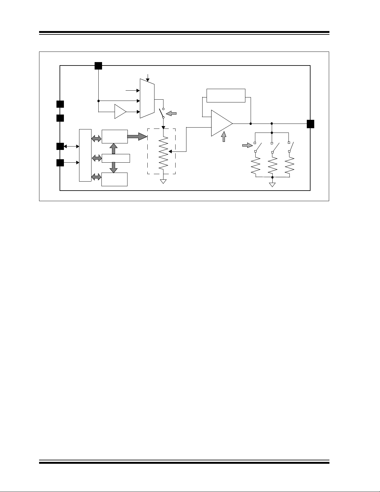
Block Diagram
V
REF
V
DD
V
SS
SDA
SCL
C Interface Logic
2
I
V
DD
Buffer
DAC
Register
EEPROM
Control
Logic
V
REF1:VREF0
Reference
Selection
Resistor Ladder
V
RL
PD1:PD0
V
W
Gain (1x or 2x)
(G = 0 or 1)
Op
Amp
PD1:PD0
V
OUT
1kΩ
640 kΩ
125 kΩ
DS22272A-page 2 © 2011 Microchip Technology Inc.
Page 3

MCP4706/4716/4726
1.0 ELECTRICAL CHARACTERISTICS
Absolute Maximum Ratings †
Voltage on VDD with respect to VSS................ -0.6V to +6.5V
Voltage on all pins with respect to V
................................................................................
Input clamp current, I
....................................................................................±20 mA
Output clamp current, I
....................................................................................±20 mA
Maximum input current source/sunk by SDA, SCL pins
........................................................................................2 mA
Maximum output current sunk by SDA Output pin
......................................................................................25 mA
Maximum current out of V
Maximum current into V
Maximum current sourced by the V
Maximum current sunk by the V
Maximum current sunk by the V
Package power dissipation (T
SOT-23-6 .......................................................452 mW
DFN-6 ..........................................................1098 mW
Storage temperature.....................................-65°C to +150°C
Ambient temperature with power applied
......................................................................-55°C to +125°C
ESD protection on all pins ....................................≥ 6kV (HBM)
....................................................................................≥ 400V (MM)
Maximum Junction Temperature (T
(VI < 0, VI > VDD, VI)
IK
(VO < 0 or VO > VDD)
OK
pin...................................50 mA
SS
pin......................................50 mA
DD
SS
-0.3V to VDD + 0.3V
pin ..................40 mA
OUT
pin........................40 mA
OUT
pin.........................40 µA
REF
= +50°C, TJ = +150°C)
A
) ......................... +150°C
J
† Notice: Stresses above those listed under “Maximum
Ratings” may cause permanent damage to the device. This is
a stress rating only and functional operation of the device at
those or any other conditions above those indicated in the
operational listings of this specification is not implied.
Exposure to maximum rating condit ions f or ext ended periods
may affect device reliability.
© 2011 Microchip Technology Inc. DS22272A-page 3
Page 4
MCP4706/4716/4726
ELECTRICAL CHARACTERISTICS
Electrical Specifications: Unless otherwise indicated, VDD = 2.7V to 5.5V, VSS = 0V , RL = 5 kΩ from V
= -40°C to +125°C. Typical values at +25°C.
Parameters Symbol Min Typical Max Units Conditions
Power Requirements
Input Voltage V
Input Current I
DD
DD
2.7 — 5.5 V
— 210 400 µA V
REF1:VREF0
SCL = SDA = V
volatile DAC Register = 0x000
— 210 400 µA V
REF1:VREF0
SCL = SDA = V
volatile DAC Register = 0x000
Power-Down Current I
Power-On Reset
V
DDP
POR
— 0.09 2 µA PD1:PD0 = ‘01’ (Note 6),
not connected
V
OUT
— 2.2 — V RAM retent ion voltage, (V
Threshold
Power-Up Ramp Rate V
Note 1: This parameter is ensured by design and is not 100% tested.
2: This gain error does not include offset error. See Section 2 for more details in plots.
3: Within 1/2 LSb of final value when code changes from 1/4 to 3/4 of FSR. (Example: 400h to C00h in 12- bit device).
4: The power-up ramp rate affects on uploading the EEPROM contents to the DAC register. It measures the rise of V
over time.
5: This parameter is ensured by characterization, and not 100% tested.
6: The PD1:PD0 = ‘10’, and ‘11’ configurations should have the same current.
7: V
= 5.5V.
DD
RAMP
1——V/S(Note 1, Note 4)
to GND, CL = 100 pF , TA
OUT
= ‘00’,
, V
SS
= ‘11’, V
, V
SS
is unloaded,
OUT
= VDD,
REF
is unloaded,
OUT
RAM
) < V
POR
DD
DS22272A-page 4 © 2011 Microchip Technology Inc.
Page 5
MCP4706/4716/4726
ELECTRICAL CHARACTERISTICS (CONTINUED)
Electrical Specifications: Unless otherwise indicated, VDD = 2.7V to 5.5V, VSS = 0V , RL = 5 kΩ from V
= -40°C to +125°C. Typical values at +25°C.
Parameters Symbol Min Typical Max Units Conditions
DC Accuracy
Offset Error V
Offset Error Tempera-
V
ture
OS
/°C — ±1 — ppm/°C -40°C to +25°C
OS
— ±2 — ppm/°C +25°C to +85°C
±0.02 0 .75 % of FSR Code = 0x000h
V
REF1:VREF0
Coefficient
Zero Scale Error EZS — 0.13 2.0 LSb MCP4706, Code = 0x00h
— 0.52 7.7 LSb MCP4716, Co de = 0x000h
— 2.05 30.8 LSb MCP4726, Code = 0x000h
Full Scale Error E
— 0.3 5.2 LSb MCP4706, Code = 0xFFh
FS
— 1.1 20.5 LSb MCP4716, Code = 0x3FFh
— 4.1 82.0 LSb MCP4726, Code = 0xFFFh
Gain Error
(Note 2)
g
E
-2 -0.10 2 % of FSR MCP4706, Code = 0xFFh
V
REF1:VREF0
-2 -0.10 2 % of FSR MCP4716, Code = 0x3FFh
V
REF1:VREF0
-2 -0.10 2 % of FSR MCP4726, Code = 0xFFFh
V
REF1:VREF0
Gain Error Drift ΔG/°C — -3 — ppm/°C
Resolution n 8 bits MCP4706
10 bits MCP4716
12 bits MCP4726
INL Error
(Note 7)
INL -0.907 ±0.125 +0.907 LSb MCP4706 (codes: 6 to 250)
-3.625 ±0.5 +3.625 LSb MCP4716 (codes: 25 to 1000)
-14.5 ±2 +14.5 LSb MCP4726 (codes: 100 to 4000)
DNL Error
(Note 7)
DNL -0.05 ±0.0125 +0.05 LSb MCP4706 (codes: 6 to 250)
-0.188 ±0.05 +0.188 LSb MCP4716 (codes: 25 to 1000)
-0.75 ±0.2 +0.75 LSb MCP4726 (codes: 100 to 4000)
Note 1: This parameter is ensured by design and is not 100% tested.
2: This gain error does not include offset error. See Section 2 for more details in plots.
3: Within 1/2 LSb of final value when code changes from 1/4 to 3/4 of FSR. (Example: 400h to C00h in 12- bit device).
4: The power-up ramp rate affects on uploading the EEPROM contents to the DAC register. It measures the rise of V
over time.
5: This parameter is ensured by characterization, and not 100% tested.
6: The PD1:PD0 = ‘10’, and ‘11’ configurations should have the same current.
7: V
= 5.5V.
DD
to GND, CL = 100 pF , TA
OUT
= ‘00’, G = ‘0’
= ‘00’, G = ‘0’
= ‘00’, G = ‘0’
= ‘00’, G = ‘0’
DD
© 2011 Microchip Technology Inc. DS22272A-page 5
Page 6
MCP4706/4716/4726
ELECTRICAL CHARACTERISTICS (CONTINUED)
Electrical Specifications: Unless otherwise indicated, VDD = 2.7V to 5.5V, VSS = 0V , RL = 5 kΩ from V
= -40°C to +125°C. Typical values at +25°C.
Parameters Symbol Min Typical Max Units Conditions
Output Amplifier
Minimum Output Volt-
V
OUT(MIN)
— 0.01 — V Output Amplifier’s minimum drive
age
Maximum Output
Voltage
Phase Margin PM — 66 — Degree
V
OUT(MAX)
—VDD –
0.04
— V Output Amplifier’s maximum drive
= 400 pF, R
C
L
(°)
Slew Rate SR — 0.55 — V/µs
Short Circuit Current I
Settling Time t
SETTLING
Power Down Output
Disable Time Delay
T
SC
PDD
71524mA
—6—µsNote 3
— 1 — µs PD1:PD0 = “00” -> ‘11’, ‘10’, or ‘01’
started from falling edge SCL at end of
ACK bit.
= V
V
OUT
OUT
connected.
Power Down Output
Enable Time Delay
— 10.5 — µs PD1:PD0 = ‘11’, ‘10’, or ‘01’ -> “00”
T
PDE
started from falling edge SCL at end of
ACK bit.
Volatile DAC Register = FFh,
=10mV. V
V
OUT
External Reference (V
Input Range V
) (Note 1)
REF
0.04 — VDD -
REF
V Buffered Mode
0.04
V Unbuffered Mode
Input Impedance R
0—V
— 210 — kΩ Unbuffered Mode
VREF
DD
Input Capacitance C_REF — 29 — pF Unbuffered Mode
-3 dB Bandwidth — 86.5 — kHz V
—67.7— kHzV
Total Harmonic Distor-
THD — -73 — dB V
tion
= 2.048V ± 0.1V,
REF
V
REF1:VREF0
= 2.048V ± 0.1V,
REF
V
REF1:VREF0
= 2.048V ± 0.1V,
REF
V
REF1:VREF0
Frequency = 1 kHz
Dynamic Performance (Note 1)
Major Code Transition
Glitch
— 45 — nV-s 1 LSb change around major carry
(800h to 7FFh)
Digital Feedthrough — <10 — nV-s
Note 1: This parameter is ensured by design and is not 100% tested.
2: This gain error does not include offset error. See Section 2 for more details in plots.
3: Within 1/2 LSb of final value when code changes from 1/4 to 3/4 of FSR. (Example: 400h to C00h in 12- bit device).
4: The power-up ramp rate affects on uploading the EEPROM contents to the DAC register. It measures the rise of V
over time.
5: This parameter is ensured by characterization, and not 100% tested.
6: The PD1:PD0 = ‘10’, and ‘11’ configurations should have the same current.
7: V
= 5.5V.
DD
to GND, CL = 100 pF , TA
OUT
= ∞
L
- 10 mV. V
OUT
=‘10’, G = ‘0’
=‘10’, G = ‘1’
=‘10’, G = ‘0’,
not
OUT
not connected.
DD
DS22272A-page 6 © 2011 Microchip Technology Inc.
Page 7
MCP4706/4716/4726
ELECTRICAL CHARACTERISTICS (CONTINUED)
Electrical Specifications: Unless otherwise indicated, VDD = 2.7V to 5.5V, VSS = 0V , RL = 5 kΩ from V
= -40°C to +125°C. Typical values at +25°C.
Parameters Symbol Min Typical Max Units Conditions
Digital Interface
Output Low V oltage VOL ——0.4 V IOL = 3 mA
Input High Voltage
VIH 0.7V
—— V
DD
(SDA and SCL Pins)
Input Low Voltage
V
— —0.3VDDV
IL
(SDA and SCL Pins)
Input Leakage I
— — ±1 µA SCL = SDA = V
LI
SCL = SDA = V
Pin Capacitance C
—— 3 pF (Note 5)
PIN
EEPROM
EEPROM Write Time T
WRITE
—2550ms
Data Retention — 200 — Years At +25°C, (Note 1)
Endurance 1 — — Million
At +25°C, (Note 1)
Cycles
Note 1: This parameter is ensured by design and is not 100% tested.
2: This gain error does not include offset error. See Section 2 for more details in plots.
3: Within 1/2 LSb of final value when code changes from 1/4 to 3/4 of FSR. (Example: 400h to C00h in 12- bit device).
4: The power-up ramp rate affects on uploading the EEPROM contents to the DAC register. It measures the rise of V
over time.
5: This parameter is ensured by characterization, and not 100% tested.
6: The PD1:PD0 = ‘10’, and ‘11’ configurations should have the same current.
7: V
= 5.5V.
DD
to GND, CL = 100 pF , TA
OUT
or
SS
DD
DD
© 2011 Microchip Technology Inc. DS22272A-page 7
Page 8

MCP4706/4716/4726
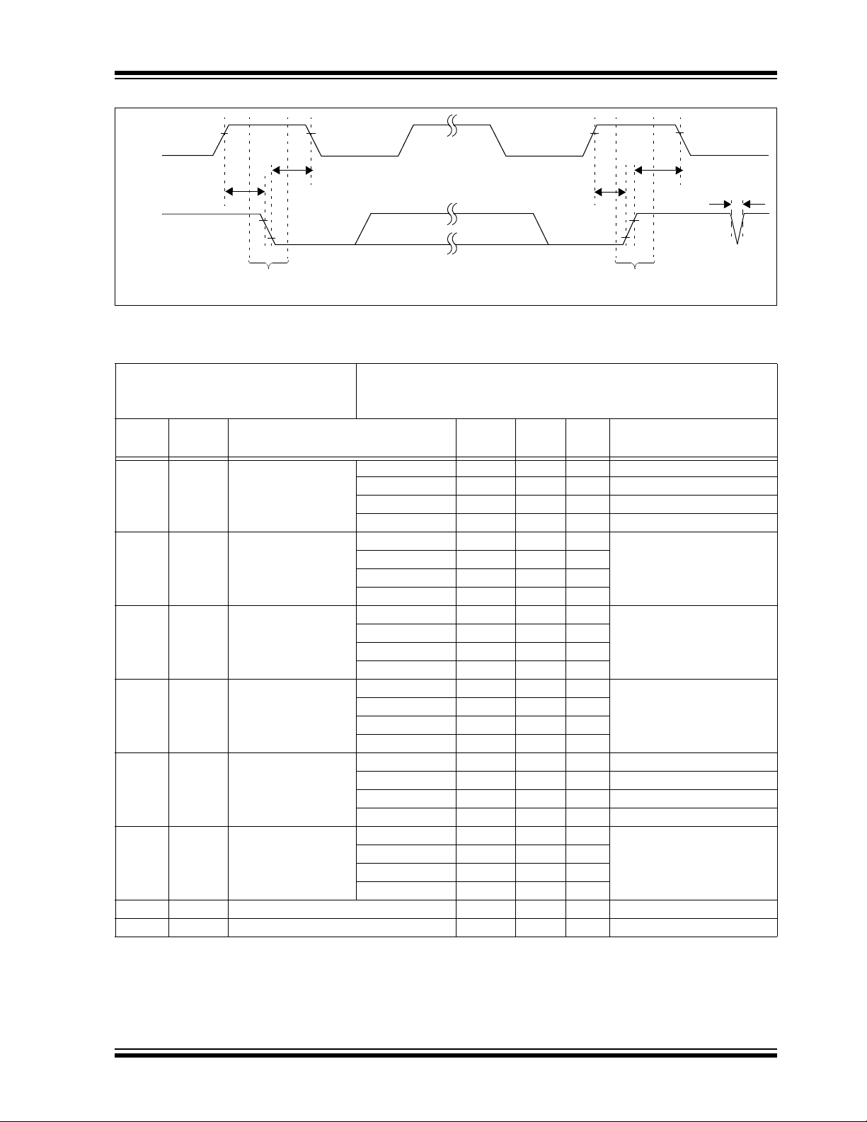
1.1 I2C Mode Timing Waveforms and Requirements
VDD
t
PORD
V
POR
t
BORD
(V
BOR
)
SCL
SDA
V
OUT
V
IH
2
I
C Interface is operational
FIGURE 1-1: Power-On and Brown-Out Reset Waveforms.
ACK Stop Start ACK
SDA
SCL
t
t
PDE
V
OUT
FIGURE 1-2: I2C Power-Down Command Timing.
V
pulled down by internal
OUT
500 kΩ (typical) resistor
PDD
V
IH
TABLE 1-1: RESET TIMING
Standard Operating Conditions (unless otherwise specified)
Timing Characteristics
Operating Temperature –40°C ≤ T
All parameters apply across the specified operating ranges unless noted.
= +2.7V to 5.5V, 5 kΩ, 10 kΩ, 50 kΩ, 100kΩ devices.
V
DD
Typical specifications represent values for V
≤ +125°C (extended)
A
= 5.5V, TA = +25°C.
DD
Parameters Sym Min Typ Max Units Conditions
Power Up Reset
Delay
Brown Out Reset
Delay
Power Down Disable
Time Delay
t
— 60 — µs Monitor ACK bit response to ensure device
PORD
responds to command.
—1—µsVDD transitions from V
t
BORD
—2.5— µsVDD = 5V
T
PDD
V
OUT
driven to V
PD1:PD0 → ‘00’ (from ‘01’, ‘10’, or ‘11’),
from falling edge SCL at end of ACK bit.
—5—µsV
DD
= 3V
PD1:PD0 → ‘00’ (from ‘01’, ‘10’, or ‘11’),
from falling edge SCL at end of ACK bit.
Power Down Enable
Time Delay
— 10.5 — µs PD1:PD0 → ‘01’, ‘10’, or ‘11’ (from ‘00’),
T
PDE
from falling edge SCL at end of ACK bit.
OUT
DD(MIN)
disabled
→ > V
POR
DS22272A-page 8 © 2011 Microchip Technology Inc.
Page 9
MCP4706/4716/4726
VIH
SCL
91
90
SDA
VIL
START
Condition
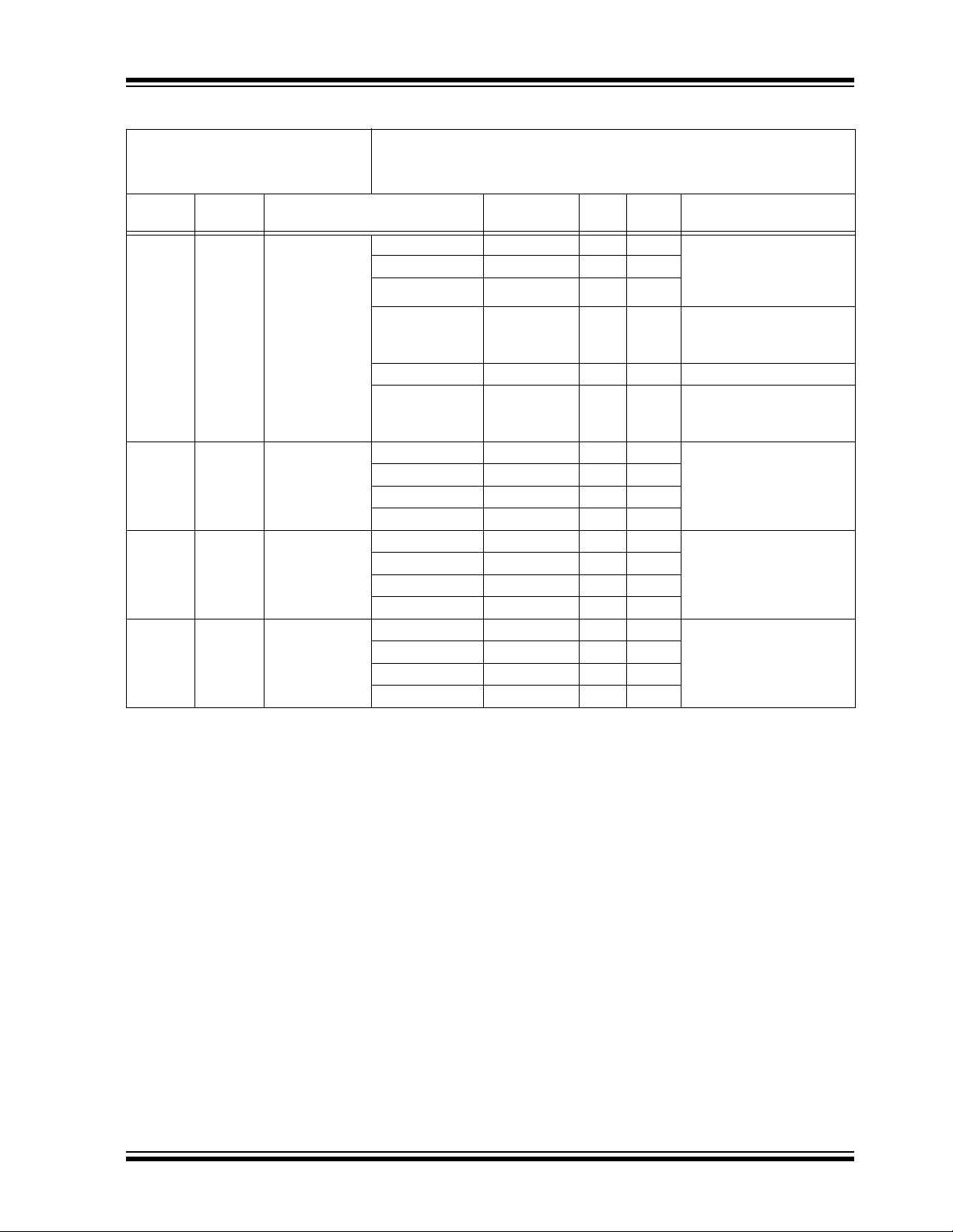
FIGURE 1-3: I2C Bus Start/Stop Bits Timing Waveforms.
TABLE 1-2: I
I2C AC Characteristics
Param.
No.
D102 C
Symbol Characteristic Min Max Units Conditions
90 T
91 T
92 T
93 T
94 T
95 T
2
C BUS START/STOP BITS REQUIREMENTS
Standard Operating Conditions (unless otherwise specified)
Operating Temperature –40°C ≤ T
Operating Voltage V
SCL pin Frequency Standard Mode 0 100 kHz Cb = 400 pF, 2.7V - 5.5V
F
SCL
DD range is described in Electrical characteristics
Fast Mode 0 400 kHz Cb = 400 pF, 2.7V - 5.5V
High-S pe ed 1.7 0 1.7 MHz C
High-S pe ed 3.4 0 3.4 MHz Cb = 100 pF, 4.5V - 5.5V
Bus capaciti v e
b
loading
100 kHz mode — 400 pF
400 kH z mode — 400 pF
1.7 MHz mode — 400 pF
3.4 MHz mode — 100 pF
SU:STA START condition 100 kHz mode 4700 — ns Only relevant for repeated
Setup time 400 kHz mode 600 — ns
1.7 MHz mode 160 — ns
3.4 MHz mode 160 — ns
HD:STA START condition 100 kHz mode 4000 — ns After this period the first
Hold time 400 kHz mode 600 — ns
1.7 MHz mode 160 — ns
3.4 MHz mode 160 — ns
SU:STO STOP condition 100 kHz mode 4000 — ns
Setup time 400 kHz mode 600 — ns
1.7 MHz mode 160 — ns
3.4 MHz mode 160 — ns
HD:STO STOP condition 100 kHz mode 4000 — ns
Hold time 400 kHz mode 600 — ns
1.7 MHz mode 160 — ns
3.4 MHz mode 160 — ns
HVC to SCL Setup time 25 — uS High Voltage Commands
HVCSU
SCL to HVC Hold time 25 — uS High Voltage Commands
HVCHD
93
92
111
STOP
Condition
A ≤ +125°C (Extended)
= 400 pF, 4.5V - 5.5V
b
START condition
clock pulse is generated
© 2011 Microchip Technology Inc. DS22272A-page 9
Page 10

MCP4706/4716/4726
103
100
101
SCL
90
91 92
106
107
SDA
In
109
SDA
Out
109
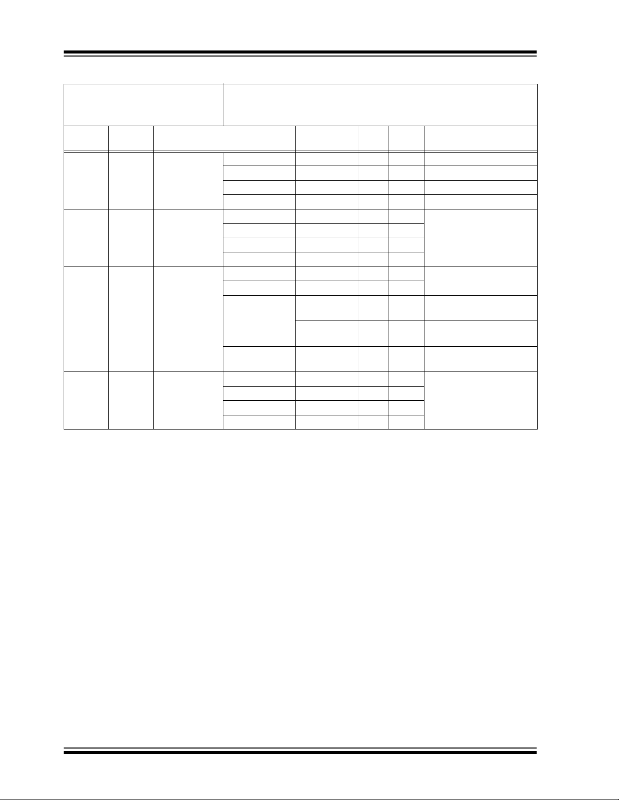
FIGURE 1-4: I2C Bus Data Timing.
TABLE 1-3: I2C BUS DATA REQUIREMENTS (SLAVE MODE)
I2C AC Characteristics
Param.
Sym Characteristic Min Max Units Conditions
No.
100 T
101 T
HIGH
LOW Clock low time 100 kHz mode 4700 — ns 2.7V-5.5V
Clock high time 100 k Hz mode 4000 — ns 2.7V-5.5V
Note 1: As a transmitter, the device must provide this internal minimum delay time to bridge the undefined region
(minimum 300 ns) of the falling edge of SCL to avoid uninten ded gene ration of START or STOP conditions.
2: A fast-mode (400 kHz) I
requirement t
≥ 250 ns must then be met. This will automatically be the case if the device does not
SU;DAT
stretch the LOW period of the SCL signal . If suc h a de vic e do es stretc h the LO W peri od of the SCL sig nal ,
it must output the next data bit to the SDA line.
max.+t
T
R
= 1000 + 250 = 1250 ns (according to the standard-mode I2C bus specification) before
SU;DAT
the SCL line is released.
3: The MCP47X6 device must provide a data hold time to bridge the undefined part between V
the falling edge of the SCL s ignal. This specificati on is not a p art of the I
in order to ensure that the output data will meet the setup and hold specifications for the receiving device.
4: Use C
in pF for the calculations.
b
5: Not Tested. This parameter ensured by characterization.
6: A Master Transmitter must provide a delay to ensure that difference between SDA and SCL fall times do
not unintentionally create a Start or Stop condition.
If this parameter is too short, it can create an unintentional Start or Stop condition to other devices on the
2
I
C bus line. If this parameter is too long, the Data Input Setup (T
affected.
Data Input: This parameter must be longer than t
Data Output: This parameter is characterized, and tested indirectly by testing T
7: Ensured by the T
3.4 MHz specification test.
AA
8: The specification is not part of the I
Standard Operating Conditions (unless otherwise specified)
Operating Temperature –40°C ≤ T
Operating Voltage V
range is described in Electrical characteristics
DD
A ≤ +125°C (Extended)
400 kHz mode 600 — ns 2.7V-5.5V
1.7 MHz mode 120 ns 4.5V-5.5V
3.4 MHz mode 60 — ns 4.5V-5.5V
400 kHz mode 1300 — ns 2.7V-5. 5V
1.7 MHz mode 320 ns 4.5V-5.5V
3.4 MHz mode 160 — ns 4.5V-5.5V
2
C-bus device can be used in a standard-mode (100 kHz) I2C-bus system, but the
2
C specification, but m ust be tested
) or Clock Low time (T
SU:DAT
.
SP
2
C specification. TAA = T
HD:DAT
+ T
FSDA
(or T
102
RSDA
110
).
and VIL of
IH
LOW
parameter.
AA
) can be
DS22272A-page 10 © 2011 Microchip Technology Inc.
Page 11
MCP4706/4716/4726
TABLE 1-3: I2C BUS DATA REQUIREMENTS (SLAVE MODE) (CONTINUED)
I2C AC Characteristics
Param.
Sym Characteristic Min Max Units Conditions
No.
(5)
T
SCL rise time 100 kHz mo de — 1000 ns Cb is specified to be from
102A
102B
103A
103B
(5)
(5)
(5)
RSCL
T
SDA rise time 100 kHz mode — 1000 ns Cb is specified to be from
RSDA
T
SCL fall time 100 kH z mode — 300 ns Cb is specified to be from
FSCL
T
SDA fall time 100 kHz mode — 300 ns Cb is specified to be from
FSDA
Note 1: As a transmitter, the device must provide this internal minimum delay time to bridge the undefined region
(minimum 300 ns) of the falling edge of SCL to avoid uninten ded gene ration of START or STOP conditions.
2: A fast-mode (400 kHz) I
requirement t
≥ 250 ns must then be met. This will automatically be the case if the device does not
SU;DAT
stretch the LOW period of the SCL sig nal . If such a de vic e do es stretch the LOW period of the SCL signal,
it must output the next data bit to the SDA line.
max.+t
T
R
= 1000 + 250 = 1250 ns (according to the standard-mode I2C bus specification) before
SU;DAT
the SCL line is released.
3: The MCP47X6 device must provide a data hold time to bridge the undefined part between V
the falling edge of the SCL s ignal. This specificati on is not a p art of the I
in order to ensure that the output data will meet the setup and hold specifications for the receiving device.
4: Use C
in pF for the calculations.
b
5: Not Tested. This parameter ensured by characterization.
6: A Master Transmitter must provide a delay to ensure that difference between SDA and SCL fall times do
not unintentionally create a Start or Stop condition.
If this parameter is too short, it can create an unintentional Start or Stop condition to other devices on the
2
C bus line. If this parameter is too long, the Data Input Setup (T
I
affected.
Data Input: This parameter must be longer than t
Data Output: This parameter is characterized, and tested indirectly by testing T
7: Ensured by the T
3.4 MHz specification test.
AA
8: The specification is not part of the I2C specification. TAA = T
Standard Operating Conditions (unless otherwise specified)
Operating Temperature –40°C ≤ T
Operating Voltage V
range is described in Electrical characteristics
DD
400 kHz mode 20 + 0.1Cb 300 ns
1.7 MHz mode 20 80 ns
A ≤ +125°C (Extended)
10 to 400 pF (100 pF
maximum for 3.4 MHz
mode)
1.7 MHz mode 20 160 ns After a Repeated Start
condition or an
Acknowledge bit
3.4 MHz mode 10 40 ns
3.4 MHz mode 10 80 ns After a Repeated Start
condition or an
Acknowledge bit
400 kHz mode 20 + 0.1Cb 300 ns
1.7 MHz mode 20 160 ns
10 to 400 pF (100 pF max
for 3.4 MHz mode)
3.4 MHz mode 10 80 ns
400 kHz mode 20 + 0.1Cb 300 ns
1.7 MHz mode 20 80 ns
10 to 400 pF (100 pF max
for 3.4 MHz mode)
3.4 MHz mode 10 40 ns
(4)
400 kHz mode 20 + 0.1Cb
300 ns
1.7 MHz mode 20 160 ns
10 to 400 pF (100 pF max
for 3.4 MHz mode)
3.4 MHz mode 10 80 ns
2
C-bus device can be used in a standard-mode (100 kHz) I2C-bus system, but the
and VIL of
AA
).
IH
) can be
LOW
parameter.
.
SP
HD:DAT
2
C specification, but m ust be tested
) or Clock Low time (T
SU:DAT
+ T
FSDA
(or T
RSDA
© 2011 Microchip Technology Inc. DS22272A-page 11
Page 12
MCP4706/4716/4726
TABLE 1-3: I2C BUS DATA REQUIREMENTS (SLAVE MODE) (CONTINUED)
I2C AC Characteristics
Param.
Sym Characteristic Min Max Units Conditions
No.
106 T
HD:DAT
Data input hold
time
107 T
SU:DAT
Data input setup
time
109 T
AA
Output valid
from clock
110 T
BUF Bus free time 100 kHz mode 4700 — ns Time the bus must be free
Note 1: As a transmitter, the device must provide this internal minimum delay time to bridge the undefined region
(minimum 300 ns) of the falling edge of SCL to avoid uninten ded gene ration of START or STOP conditions.
2: A fast-mode (400 kHz) I
requirement t
≥ 250 ns must then be met. This will automatically be the case if the device does not
SU;DAT
stretch the LOW period of the SCL signal . If suc h a de vic e do es stretc h the LO W peri od of the SCL sig nal ,
it must output the next data bit to the SDA line.
max.+t
T
R
= 1000 + 250 = 1250 ns (according to the standard-mode I2C bus specification) before
SU;DAT
the SCL line is released.
3: The MCP47X6 device must provide a data hold time to bridge the undefined part between V
the falling edge of the SCL s ignal. This specificati on is not a p art of the I
in order to ensure that the output data will meet the setup and hold specifications for the receiving device.
4: Use C
in pF for the calculations.
b
5: Not Tested. This parameter ensured by characterization.
6: A Master Transmitter must provide a delay to ensure that difference between SDA and SCL fall times do
not unintentionally create a Start or Stop condition.
If this parameter is too short, it can create an unintentional Start or Stop condition to other devices on the
I2C bus line. If this parameter is too long, the Data Input Setup (T
affected.
Data Input: This parameter must be longer than t
Data Output: This parameter is characterized, and tested indirectly by testing T
7: Ensured by the TAA 3.4 MHz specification test.
8: The specification is not part of the I
Standard Operating Conditions (unless otherwise specified)
Operating Temperature –40°C ≤ T
Operating Voltage V
range is described in Electrical characteristics
DD
A ≤ +125°C (Extended)
100 kHz mode 0 — ns 2.7V-5.5V, Note 6
400 kHz mode 0 — ns 2.7V-5.5V, Note 6
1.7 MHz mode 0 — ns 4.5V-5.5V, Note 6
3.4 MHz mode 0 — ns 4.5V-5.5V, Note 6
100 kHz mode 250 — ns Note 2
400 kHz mode 100 — ns
1.7 MHz mode 10 — ns
3.4 MHz mode 10 — ns
100 kHz mode — 3750 ns Note 1, Note 8
400 kHz mode — 1200 ns
1.7 MHz mode — 150 ns Cb = 100 pF,
Note 1, Note 7, Note 8
— 310 ns Cb = 400 pF,
Note 1, Note 5, Note 8
3.4 MHz mode — 150 ns Cb = 100 pF,
Note 1, Note 8
400 kHz mode 1300 — ns
1.7 MHz mode N.A. — ns
before a new transmission
can start
3.4 MHz mode N.A. — ns
2
C-bus device can be used in a standard-mode (100 kHz) I2C-bus system, but the
and VIL of
AA
).
IH
) can be
LOW
parameter.
2
C specification. TAA = T
.
SP
HD:DAT
2
C specification, but m ust be tested
) or Clock Low time (T
SU:DAT
+ T
FSDA
(or T
RSDA
DS22272A-page 12 © 2011 Microchip Technology Inc.
Page 13
MCP4706/4716/4726
TABLE 1-3: I2C BUS DATA REQUIREMENTS (SLAVE MODE) (CONTINUED)
I2C AC Characteristics
Param.
Sym Characteristic Min Max Units Conditions
No.
111 TSP Input filter spike
suppression
(SDA and SCL)
Note 1: As a transmitter, the device must provide this internal minimum delay time to bridge the undefined region
(minimum 300 ns) of the falling edge of SCL to avoid uninten ded gene ration of START or STOP conditions.
2: A fast-mode (400 kHz) I
requirement t
≥ 250 ns must then be met. This will automatically be the case if the device does not
SU;DAT
stretch the LOW period of the SCL sig nal . If such a de vic e do es stretch the LOW period of the SCL signal,
it must output the next data bit to the SDA line.
max.+t
T
R
= 1000 + 250 = 1250 ns (according to the standard-mode I2C bus specification) before
SU;DAT
the SCL line is released.
3: The MCP47X6 device must provide a data hold time to bridge the undefined part between V
the falling edge of the SCL s ignal. This specificati on is not a p art of the I
in order to ensure that the output data will meet the setup and hold specifications for the receiving device.
4: Use C
in pF for the calculations.
b
5: Not Tested. This parameter ensured by characterization.
6: A Master Transmitter must provide a delay to ensure that difference between SDA and SCL fall times do
not unintentionally create a Start or Stop condition.
If this parameter is too short, it can create an unintentional Start or Stop condition to other devices on the
2
C bus line. If this parameter is too long, the Data Input Setup (T
I
affected.
Data Input: This parameter must be longer than t
Data Output: This parameter is characterized, and tested indirectly by testing T
7: Ensured by the T
3.4 MHz specification test.
AA
8: The specification is not part of the I2C specification. TAA = T
Standard Operating Conditions (unless otherwise specified)
Operating Temperature –40°C ≤ T
Operating Voltage V
range is described in Electrical characteristics
DD
A ≤ +125°C (Extended)
100 kHz mode — 50 ns NXP Spec states N.A.
400 kHz mode — 50 ns
1.7 MHz mode — 10 ns Spike suppression
3.4 MHz mode — 10 ns Spike suppression
— — — ns Standard Mode,
(Not Applicable)
50 (typ) — — ns Fast Mode
10 (typ) — — ns High Speed Mode 1.7
10 (typ) — — ns High Speed Mode 3.4
2
C-bus device can be used in a standard-mode (100 kHz) I2C-bus system, but the
and VIL of
AA
).
IH
) can be
LOW
parameter.
.
SP
HD:DAT
2
C specification, but m ust be tested
) or Clock Low time (T
SU:DAT
+ T
FSDA
(or T
RSDA
© 2011 Microchip Technology Inc. DS22272A-page 13
Page 14

MCP4706/4716/4726
TEMPERATURE CHARACTERISTICS
Electrical Specifications: Unless otherwise indicated, VDD= +2.7V to +5.5V, VSS= GND.
Parameters Symbol Min Typical Max Units Conditions
Temperature Ranges
Specified Temperature Range T
Operating Temperature Range T
Storage Temperature Range T
Thermal Package Resistances
Thermal Resistance, 6L-SOT-23 θ
Thermal Resistance, 6L-DFN (2 x 2) θ
Note 1: The MCP47X6 devices operate over this extended temperature range, but with reduced performance.
Operation in this range must not cause T
A
A
A
JA
JA
-40 — +125 °C
-40 — +125 °C Note 1
-65 — +150 °C
—190—°C/W
—91—°C/W
to exceed the Maximum Junction Temperature of +150°C.
J
DS22272A-page 14 © 2011 Microchip Technology Inc.
Page 15
MCP4706/4716/4726
2.0 TYPICAL PERFORMANCE CURVES
Note: The graphs and tables provided fol lowing this note are a st atistical summary b as ed on a l im ite d n um ber of
samples and are provided for informational purposes only. The performance characteristics listed herein
are not tested or guaranteed. In some graphs or tables, the data presented may be outside the specified
operating range (e.g., outside specified power supply range) and therefore outside the warranted range.
Note: Unless otherwise indicate d, TA = +25°C, VDD = 5V , VSS = 0V, VRL = Internal, Gain = x1, R
12
-40C
+25C
+85C
8
+125C
4
0
-4
INL Error (LSb)
-8
-12
0 1024 2048 3072 4096
Volatile DAC Register Code
FIGURE 2-1: INL vs. Code (code = 100 to
4000) and Temperature (MCP4726).
V
DD
-1
INL Error (LSb)
= 5V, V
3
-40C
+25C
+85C
2
+125C
1
0
REF1:VREF0
= ‘00’.
12
-40C
+25C
+85C
8
+125C
4
0
-4
INL Error (LSb)
-8
-12
0 1024 2048 3072 4096
Volatile DAC Register Code
FIGURE 2-4: INL vs. Code (code = 100 to
4000) and Temperature (MCP4726).
V
DD
-1
INL Error (LSb)
= 2.7V, V
3
-40C
+25C
+85C
2
+125C
1
0
REF1:VREF0
= ‘00’.
= 5 kΩ, C
L
= 100 pF .
L
-2
-3
0 128 256 384 512 640 768 896 1024
Volatile DAC Register Code
FIGURE 2-2: INL vs. Code (code = 25 to
1000) and Temperature (MCP4716).
V
= 5V, V
DD
INL Error (LSb)
-0.5
-1.0
1.0
0.5
0.0
REF1:VREF0
-40C
+25C
+85C
+125C
0 32 64 96 128 160 192 224 256
= ‘00’.
Volatile DAC Register Code
FIGURE 2-3: INL vs. Code (code = 6 to
250) and Temperature (MCP4706).
V
= 5V, V
DD
REF1:VREF0
= ‘00’.
-2
-3
0 128 256 384 512 640 768 896 1024
Volatile DAC Register Code
FIGURE 2-5: INL vs. Code (code = 25 to
1000) and Temperature (MCP4716).
V
= 2.7V, V
DD
1.0
0.5
0.0
INL Error (LSb)
-0.5
-1.0
0 32 64 96 128 160 192 224 256
REF1:VREF0
-40C
+25C
+85C
+125C
Volatile DAC Register Code
= ‘00’.
FIGURE 2-6: INL vs. Code (code = 6 to
250) and Temperature (MCP4706).
V
= 2.7V, V
DD
REF1:VREF0
= ‘00’.
© 2011 Microchip Technology Inc. DS22272A-page 15
Page 16

MCP4706/4716/4726
Note: Unless otherwise indicated, TA = +25°C, VDD = 5V, VSS = 0V, VRL = Internal, Gain = x1, RL = 5 kΩ, CL = 100 pF.
0.4
0.3
0.2
0.1
0.0
-0.1
DNL Error (LSb)
-0.2
-40C
+25C
-0.3
+85C
+125C
-0.4
0 1024 2048 3072 4096
Volatile DAC Register Code
FIGURE 2-7: DNL vs. Code (code = 100
to 4000) and Temperature (MCP4726).
V
DD
= 5V, V
0.3
REF1:VREF0
= ‘00’.
0.4
0.3
0.2
0.1
0.0
-0.1
DNL Error (LSb)
-0.2
-40C
+25C
-0.3
+85C
+125C
-0.4
0 1024 2048 3072 4096
Volatile DAC Register Code
FIGURE 2-10: DNL vs. Code (code = 100
to 4000) and Temperature (MCP4726).
V
DD
= 2.7V, V
0.3
REF1:VREF0
= ‘00’.
0.2
0.1
0.0
-0.1
DNL Error (LSb)
-40C
-0.2
+25C
+85C
+125C
-0.3
0 128 256 384 512 640 768 896 1024
Volatile DAC Register Code
FIGURE 2-8: DNL vs. Code (code = 25 to
1000) and Temperature (MCP4716).
V
= 5V, V
DD
0.20
0.15
0.10
0.05
0.00
-0.05
DNL Error (LSb)
-0.10
-0.15
-0.20
REF1:VREF0
-40C
+25C
+85C
+125C
0 32 64 96 128 160 192 224 256
= ‘00’.
Volatile DAC Register Code
FIGURE 2-9: DNL vs. Code (code = 6 to
250) and Temperature (MCP4706).
V
= 5V, V
DD
REF1:VREF0
= ‘00’.
0.2
0.1
0.0
-0.1
DNL Error (LSb)
-40C
-0.2
+25C
+85C
+125C
-0.3
0 128 256 384 512 640 768 896 1024
Volatile DAC Register Code
FIGURE 2-11: DNL vs. Code (code = 25 to
1000) and Temperature (MCP4716).
V
= 2.7V, V
DD
0.20
0.15
0.10
0.05
0.00
-0.05
DNL Error (LSb)
-0.10
-0.15
-0.20
REF1:VREF0
-40C
+25C
+85C
+125C
0 32 64 96 128 160 192 224 256
Volatile DAC Register Code
= ‘00’.
FIGURE 2-12: DNL vs. Code (code = 6 to
250) and Temperature (MCP4706).
V
= 2.7V, V
DD
REF1:VREF0
= ‘00’.
DS22272A-page 16 © 2011 Microchip Technology Inc.
Page 17

MCP4706/4716/4726
Note: Unless otherwise indicated, TA = +25°C, VDD = 5V, VSS = 0V, VRL = Internal, Gain = x1, RL = 5 kΩ, CL = 100 pF.
2.0
2.7V
5.0V
5.5V
1.5
1.0
Zero Scale Error (LSb)
0.5
0.0
-40 -20 0 20 40 60 80 100 120
Temperature (°C)
FIGURE 2-13: Zero Scale Error (ZSE) vs.
Temperature (MCP4726).
V
= 5V, V
DD
0.5
0.4
0.3
0.2
Zero Scale Error (LSb)
0.1
0.0
REF1:VREF0
2.7V
5.0V
5.5V
-40 -20 0 20 40 60 80 100 120
= ‘00’.
Temperature (°C)
FIGURE 2-14: Zero Scale Error (ZSE) vs.
Temperature (MCP4716).
V
DD
= 5V, V
0.20
0.15
REF1:VREF0
2.7V
5.0V
5.5V
= ‘00’.
-18.0
-20.0
-22.0
-24.0
-26.0
Full Scale Error (LSb)
-28.0
2.7V
-30.0
5.0V
5.5V
-32.0
-40 -20 0 20 40 60 80 100 120
Temperature (°C)
FIGURE 2-16: Full Scale Error (FSE) vs.
Temperature (MCP4726).
V
= 2.7V, V
DD
-4.0
-5.0
-6.0
Full Scale Error (LSb)
-7.0
-8.0
-40 -20 0 20 40 60 80 100 120
REF1:VREF0
2.7V
5.0V
5.5V
= ‘00’.
Temperature (°C)
FIGURE 2-17: Full Scale Error (FSE) vs.
Temperature (MCP4716).
V
DD
-0.5
= 2.7V, V
0.0
REF1:VREF0
= ‘00’.
0.10
Zero Scale Error (LSb)
0.05
0.00
-40 -20 0 20 40 60 80 100 120
Temperature (°C)
FIGURE 2-15: Zero Scale Error (ZSE) vs.
Temperature (MCP4706).
V
= 5V, V
DD
REF1:VREF0
= ‘00’.
-1.0
Full Scale Error (LSb)
-1.5
2.7V
5.0V
5.5V
-2.0
-40 -20 0 20 40 60 80 100 120
Temperature (°C)
FIGURE 2-18: Full Scale Error (FSE) vs.
Temperature (MCP4706).
V
= 2.7V, V
DD
REF1:VREF0
= ‘00’.
© 2011 Microchip Technology Inc. DS22272A-page 17
Page 18
MCP4706/4716/4726
Note: Unless otherwise indicated, TA = +25°C, VDD = 5V, VSS = 0V, VRL = Internal, Gain = x1, RL = 5 kΩ, CL = 100 pF.
12
-40C
+25C
+85C
8
+125C
4
12
-40C
+25C
+85C
8
+125C
4
0
-4
INL Error (LSb)
-8
-12
0 1024 2048 3072 4096
Volatile DAC Register Code
FIGURE 2-19: INL vs. Code (code = 100 to
4000) and Temperature (MCP4726).
V
= 5V, V
DD
V
REF
3
2
1
0
-1
INL Error (LSb)
-2
-3
= VDD.
REF1:VREF0
-40C
+25C
+85C
+125C
0 128 256 384 512 640 768 896 1024
= ‘10’, G = ‘0’,
Volatile DAC Register Code
FIGURE 2-20: INL vs. Code (code = 25 to
1000) and Temperature (MCP4716).
V
V
DD
REF
= 5V, V
= VDD.
1.0
-40C
+25C
+85C
+125C
0.5
REF1:VREF0
= ‘10’, G = ‘0’,
0
-4
INL Error (LSb)
-8
-12
0 1024 2048 3072 4096
Volatile DAC Register Code
FIGURE 2-22: INL vs. Code (code = 100 to
4000) and Temperature (MCP4726).
V
= 2.7V, V
DD
V
= VDD.
REF
3
2
1
0
-1
INL Error (LSb)
-2
-3
0 128 256 384 512 640 768 896 1024
-40C
+25C
+85C
+125C
REF1:VREF0
Volatile DAC Register Code
= ‘10’, G = ‘0’,
FIGURE 2-23: INL vs. Code (code = 25 to
1000) and Temperature (MCP4716).
V
V
DD
REF
= 2.7V, V
= VDD.
1.0
-40C
+25C
+85C
+125C
0.5
REF1:VREF0
= ‘10’, G = ‘0’,
0.0
INL Error (LSb)
-0.5
-1.0
0 32 64 96 128 160 192 224 256
Volatile DAC Register Code
FIGURE 2-21: INL vs. Code (code = 6 to
250) and Temperature (MCP4706).
V
V
DD
REF
= 5V, V
= VDD.
REF1:VREF0
= ‘10’, G = ‘0’,
0.0
INL Error (LSb)
-0.5
-1.0
0 32 64 96 128 160 192 224 256
Volatile DAC Register Code
FIGURE 2-24: INL vs. Code (code = 6 to
250) and Temperature (MCP4706).
V
V
DD
REF
= 2.7V, V
= VDD.
REF1:VREF0
= ‘10’, G = ‘0’,
DS22272A-page 18 © 2011 Microchip Technology Inc.
Page 19
MCP4706/4716/4726
Note: Unless otherwise indicated, TA = +25°C, VDD = 5V, VSS = 0V, VRL = Internal, Gain = x1, RL = 5 kΩ, CL = 100 pF.
0.4
0.3
0.2
0.1
0.0
-0.1
DNL Error (LSb)
-0.2
-40C
+25C
-0.3
+85C
+125C
-0.4
0 1024 2048 3072 4096
Volatile DAC Register Code
FIGURE 2-25: DNL vs. Code (code = 100
to 4000) and Temperature (MCP4726).
V
V
DD
REF
= 5V, V
= VDD.
0.3
REF1:VREF0
= ‘10’, G = ‘0’,
0.4
0.3
0.2
0.1
0.0
-0.1
DNL Error (LSb)
-0.2
-40C
+25C
-0.3
+85C
+125C
-0.4
0 1024 2048 3072 4096
Volatile DAC Register Code
FIGURE 2-28: DNL vs. Code (code = 100
to 4000) and Temperature (MCP4726).
V
V
DD
REF
= 2.7V, V
= VDD.
0.3
REF1:VREF0
= ‘10’, G = ‘0’,
0.2
0.1
0.0
-0.1
DNL Error (LSb)
-40C
-0.2
+25C
+85C
+125C
-0.3
0 128 256 384 512 640 768 896 1024
Volatile DAC Register Code
FIGURE 2-26: DNL vs. Code (code = 25 to
1000) and Temperature (MCP4716).
V
= 5V, V
DD
V
REF
0.20
0.15
0.10
0.05
0.00
-0.05
DNL Error (LSb)
-0.10
-0.15
-0.20
= VDD.
REF1:VREF0
-40C
+25C
+85C
+125C
0 32 64 96 128 160 192 224 256
= ‘10’, G = ‘0’,
Volatile DAC Register Code
FIGURE 2-27: DNL vs. Code (code = 6 to
250) and Temperature (MCP4706).
V
V
DD
REF
= 5V, V
= VDD.
REF1:VREF0
= ‘10’, G = ‘0’,
0.2
0.1
0.0
-0.1
DNL Error (LSb)
-40C
-0.2
+25C
+85C
+125C
-0.3
0 128 256 384 512 640 768 896 1024
Volatile DAC Register Code
FIGURE 2-29: DNL vs. Code (code = 25 to
1000) and Temperature (MCP4716).
V
= 2.7V, V
DD
V
REF
0.20
0.15
0.10
0.05
0.00
-0.05
DNL Error (LSb)
-0.10
-0.15
-0.20
= VDD.
REF1:VREF0
-40C
+25C
+85C
+125C
0 32 64 96 128 160 192 224 256
Volatile DAC Register Code
= ‘10’, G = ‘0’,
FIGURE 2-30: DNL vs. Code (code = 6 to
250) and Temperature (MCP4706).
V
V
DD
REF
= 2.7V, V
= VDD.
REF1:VREF0
= ‘10’, G = ‘0’,
© 2011 Microchip Technology Inc. DS22272A-page 19
Page 20
MCP4706/4716/4726
Note: Unless otherwise indicated, TA = +25°C, VDD = 5V, VSS = 0V, VRL = Internal, Gain = x1, RL = 5 kΩ, CL = 100 pF.
2.0
2.7V
5.0V
5.5V
1.5
1.0
Zero Scale Error (LSb)
0.5
0.0
-40 -20 0 20 40 60 80 100 120
Temperature (°C)
FIGURE 2-31: Zero Scale Error (ZSE) vs.
Temperature (MCP4726).
V
= 5V, V
DD
V
= VDD.
REF
0.5
0.4
0.3
0.2
Zero Scale Error (LSb)
0.1
0.0
REF1:VREF0
2.7V
5.0V
5.5V
-40 -20 0 20 40 60 80 100 120
= ‘10’, G = ‘0’,
Temperature (°C)
FIGURE 2-32: Zero Scale Error (ZSE) vs.
Temperature (MCP4716).
V
V
DD
REF
= 5V, V
= VDD.
0.20
0.15
REF1:VREF0
2.7V
5.0V
5.5V
= ‘10’, G = ‘0’,
-18.0
-20.0
-22.0
-24.0
-26.0
Full Scale Error (LSb)
-28.0
2.7V
-30.0
5.0V
5.5V
-32.0
-40 -20 0 20 40 60 80 100 120
Temperature (°C)
FIGURE 2-34: Full Scale Error (FSE) vs.
Temperature (MCP4726).
V
= 2.7V, V
DD
V
= VDD.
REF
-4.0
-5.0
-6.0
Full Scale Error (LSb)
-7.0
-8.0
-40 -20 0 20 40 60 80 100 120
REF1:VREF0
2.7V
5.0V
5.5V
= ‘10’, G = ‘0’,
Temperature (°C)
FIGURE 2-35: Full Scale Error (FSE) vs.
Temperature (MCP4716).
V
V
DD
REF
-0.5
= 2.7V, V
= VDD.
0.0
REF1:VREF0
= ‘10’, G = ‘0’,
0.10
Zero Scale Error (LSb)
0.05
0.00
-40 -20 0 20 40 60 80 100 120
Temperature (°C)
FIGURE 2-33: Zero Scale Error (ZSE) vs.
Temperature (MCP4706).
V
V
DD
REF
= 5V, V
= VDD.
REF1:VREF0
= ‘10’, G = ‘0’,
-1.0
Full Scale Error (LSb)
-1.5
2.7V
5.0V
5.5V
-2.0
-40 -20 0 20 40 60 80 100 120
Temperature (°C)
FIGURE 2-36: Full Scale Error (FSE) vs.
Temperature (MCP4706).
V
V
DD
REF
= 2.7V, V
= VDD.
REF1:VREF0
= ‘10’, G = ‘0’,
DS22272A-page 20 © 2011 Microchip Technology Inc.
Page 21

MCP4706/4716/4726
Note: Unless otherwise indicated, TA = +25°C, VDD = 5V, VSS = 0V, VRL = Internal, Gain = x1, RL = 5 kΩ, CL = 100 pF.
12
-40C
+25C
+85C
8
+125C
4
12
-40C
+25C
+85C
8
+125C
4
0
-4
INL Error (LSb)
-8
-12
0 1024 2048 3072 4096
Volatile DAC Register Code
FIGURE 2-37: INL vs. Code (code = 100 to
4000) and Temperature (MCP4726).
V
= 5V, V
DD
V
REF
-1
INL Error (LSb)
-2
-3
= VDD.
3
2
1
0
REF1:VREF0
-40C
+25C
+85C
+125C
0 128 256 384 512 640 768 896 1024
= ‘11’, G = ‘0’,
Volatile DAC Register Code
FIGURE 2-38: INL vs. Code (code = 25 to
1000) and Temperature (MCP4716).
V
V
DD
REF
= 5V, V
= VDD.
1.0
-40C
+25C
+85C
+125C
0.5
REF1:VREF0
= ‘11’, G = ‘0’,
0
-4
INL Error (LSb)
-8
-12
0 1024 2048 3072 4096
Volatile DAC Register Code
FIGURE 2-40: INL vs. Code (code = 100 to
4000) and Temperature (MCP4726).
V
= 2.7V, V
DD
V
= VDD.
REF
3
2
1
0
-1
INL Error (LSb)
-2
-3
0 128 256 384 512 640 768 896 1024
-40C
+25C
+85C
+125C
REF1:VREF0
Volatile DAC Register Code
= ‘11’, G = ‘0’,
FIGURE 2-41: INL vs. Code (code = 25 to
1000) and Temperature (MCP4716).
V
V
DD
REF
= 2.7V, V
= VDD.
1.0
-40C
+25C
+85C
+125C
0.5
REF1:VREF0
= ‘11’, G = ‘0’,
0.0
INL Error (LSb)
-0.5
-1.0
0 32 64 96 128 160 192 224 256
Volatile DAC Register Code
FIGURE 2-39: INL vs. Code (code = 6 to
250) and Temperature (MCP4706).
V
V
DD
REF
= 5V, V
= VDD.
REF1:VREF0
= ‘11’, G = ‘0’,
0.0
INL Error (LSb)
-0.5
-1.0
0 32 64 96 128 160 192 224 256
Volatile DAC Register Code
FIGURE 2-42: INL vs. Code (code = 6 to
250) and Temperature (MCP4706).
V
V
DD
REF
= 2.7V, V
= VDD.
REF1:VREF0
= ‘11’, G = ‘0’,
© 2011 Microchip Technology Inc. DS22272A-page 21
Page 22

MCP4706/4716/4726
Note: Unless otherwise indicated, TA = +25°C, VDD = 5V, VSS = 0V, VRL = Internal, Gain = x1, RL = 5 kΩ, CL = 100 pF.
0.4
0.3
0.2
0.1
0.0
-0.1
DNL Error (LSb)
-0.2
-40C
+25C
-0.3
+85C
+125C
-0.4
0 1024 2048 3072 4096
Volatile DAC Register Code
FIGURE 2-43: DNL vs. Code (code = 100
to 4000) and Temperature (MCP4726).
V
V
DD
REF
= 5V, V
= VDD.
0.3
REF1:VREF0
= ‘11’, G = ‘0’,
0.4
0.3
0.2
0.1
0.0
-0.1
DNL Error (LSb)
-0.2
-40C
+25C
-0.3
+85C
+125C
-0.4
0 1024 2048 3072 4096
Volatile DAC Register Code
FIGURE 2-46: DNL vs. Code (code = 100
to 4000) and Temperature (MCP4726).
V
V
DD
REF
= 2.7V, V
= VDD.
0.3
REF1:VREF0
= ‘11’, G = ‘0’,
0.2
0.1
0.0
-0.1
DNL Error (LSb)
-40C
-0.2
+25C
+85C
+125C
-0.3
0 128 256 384 512 640 768 896 1024
Volatile DAC Register Code
FIGURE 2-44: DNL vs. Code (code = 25 to
1000) and Temperature (MCP4716).
V
= 5V, V
DD
V
REF
0.20
0.15
0.10
0.05
0.00
-0.05
DNL Error (LSb)
-0.10
-0.15
-0.20
= VDD.
REF1:VREF0
-40C
+25C
+85C
+125C
0 32 64 96 128 160 192 224 256
= ‘11’, G = ‘0’,
Volatile DAC Register Code
FIGURE 2-45: DNL vs. Code (code = 6 to
250) and Temperature (MCP4706).
V
V
DD
REF
= 5V, V
= VDD.
REF1:VREF0
= ‘11’, G = ‘0’,
0.2
0.1
0.0
-0.1
DNL Error (LSb)
-40C
-0.2
+25C
+85C
+125C
-0.3
0 128 256 384 512 640 768 896 1024
Volatile DAC Register Code
FIGURE 2-47: DNL vs. Code (code = 25 to
1000) and Temperature (MCP4716).
V
= 2.7V, V
DD
V
REF
0.20
0.15
0.10
0.05
0.00
-0.05
DNL Error (LSb)
-0.10
-0.15
-0.20
= VDD.
REF1:VREF0
-40C
+25C
+85C
+125C
0 32 64 96 128 160 192 224 256
Volatile DAC Register Code
= ‘11’, G = ‘0’,
FIGURE 2-48: DNL vs. Code (code = 6 to
250) and Temperature (MCP4706).
V
V
DD
REF
= 2.7V, V
= VDD.
REF1:VREF0
= ‘11’, G = ‘0’,
DS22272A-page 22 © 2011 Microchip Technology Inc.
Page 23

MCP4706/4716/4726
Note: Unless otherwise indicated, TA = +25°C, VDD = 5V, VSS = 0V, VRL = Internal, Gain = x1, RL = 5 kΩ, CL = 100 pF.
2.0
2.7V
5.0V
5.5V
1.5
1.0
Zero Scale Error (LSb)
0.5
0.0
-40 -20 0 20 40 60 80 100 120
Temperature (°C)
FIGURE 2-49: Zero Scale Error (ZSE) vs.
Temperature (MCP4726).
V
= 5V, V
DD
V
= VDD.
REF
0.5
0.4
0.3
0.2
Zero Scale Error (LSb)
0.1
0.0
REF1:VREF0
2.7V
5.0V
5.5V
-40 -20 0 20 40 60 80 100 120
= ‘11’, G = ‘0’,
Temperature (°C)
FIGURE 2-50: Zero Scale Error (ZSE) vs.
Temperature (MCP4716).
V
V
DD
REF
= 5V, V
= VDD.
0.20
0.15
REF1:VREF0
2.7V
5.0V
5.5V
= ‘11’, G = ‘0’,
-18.0
-20.0
-22.0
-24.0
-26.0
Full Scale Error (LSb)
-28.0
2.7V
-30.0
5.0V
5.5V
-32.0
-40 -20 0 20 40 60 80 100 120
Temperature (°C)
FIGURE 2-52: Full Scale Error (FSE) vs.
Temperature (MCP4726).
V
= 2.7V, V
DD
V
= VDD.
REF
-4.0
-5.0
-6.0
Full Scale Error (LSb)
-7.0
-8.0
-40 -20 0 20 40 60 80 100 120
REF1:VREF0
2.7V
5.0V
5.5V
= ‘11’, G = ‘0’,
Temperature (°C)
FIGURE 2-53: Full Scale Error (FSE) vs.
Temperature (MCP4716).
V
V
DD
REF
-0.5
= 2.7V, V
= VDD.
0.0
REF1:VREF0
= ‘11’, G = ‘0’,
0.10
Zero Scale Error (LSb)
0.05
0.00
-40 -20 0 20 40 60 80 100 120
Temperature (°C)
FIGURE 2-51: Zero Scale Error (ZSE) vs.
Temperature (MCP4706).
V
V
DD
REF
= 5V, V
= VDD.
REF1:VREF0
= ‘11’, G = ‘0’,
-1.0
Full Scale Error (LSb)
-1.5
2.7V
5.0V
5.5V
-2.0
-40 -20 0 20 40 60 80 100 120
Temperature (°C)
FIGURE 2-54: Full Scale Error (FSE) vs.
Temperature (MCP4706).
V
V
DD
REF
= 2.7V, V
= VDD.
REF1:VREF0
= ‘11’, G = ‘0’,
© 2011 Microchip Technology Inc. DS22272A-page 23
Page 24

MCP4706/4716/4726
Note: Unless otherwise indicated, TA = +25°C, VDD = 5V, VSS = 0V, VRL = Internal, Gain = x1, RL = 5 kΩ, CL = 100 pF.
16
2.7V
5.0V
5.5V
12
8
4
0
INL Error (LSb)
-4
-8
0 1024 2048 3072 4096
Volatile DAC Register Code
FIGURE 2-55: INL vs. Code (code = 100 to
4000) and V
V
REF1:VREF0
(2.7V, 5V, 5.5V) (MCP4726).
DD
= ‘10’, G = ‘1’, V
= VDD/2,
REF
Temp = +25°C.
3
2.7V
5.0V
5.5V
2
1
0
-1
INL Error (LSb)
-2
-3
0 128 256 384 512 640 768 896 1024
Volatile DAC Register Code
FIGURE 2-56: INL vs. Code (code = 25 to
1000) and V
V
REF1:VREF0
(2.7V, 5V, 5.5V) (MCP4716).
DD
= ‘10’, G = ‘1’, V
= VDD/2,
REF
Temp = +25°C.
1.0
2.7V
5.0V
5.5V
0.5
0.0
INL Error (LSb)
-0.5
-1.0
0 32 64 96 128 160 192 224 256
Volatile DAC Register Code
FIGURE 2-57: INL vs. Code (code = 6 to
250) and V
V
REF1:VREF0
(2.7V, 5V, 5.5V) (MCP4706).
DD
= ‘10’, G = ‘1’, V
= VDD/2,
REF
Temp = +25°C.
0.5
0.4
0.3
0.2
0.1
0.0
-0.1
-0.2
DNL Error (LSb)
-0.3
2.7V
5.0V
-0.4
5.5V
-0.5
0 1024 2048 3072 4096
Volatile DAC Register Code
FIGURE 2-58: DNL vs. Code (code = 100
to 4000) and V
V
REF1:VREF0
(2.7V, 5V, 5.5V) (MCP4726).
DD
= ‘10’, G = ‘1’, V
= VDD/2,
REF
Temp = +25°C.
0.4
0.3
0.2
0.1
0.0
DNL Error (LSb)
-0.1
2.7V
-0.2
5.0V
5.5V
-0.3
0 128 256 384 512 640 768 896 1024
Volatile DAC Register Code
FIGURE 2-59: DNL vs. Code (code = 25 to
1000) and V
V
REF1:VREF0
(2.7V, 5V, 5.5V) (MCP4716).
DD
= ‘10’, G = ‘1’, V
= VDD/2,
REF
Temp = +25°C.
0.30
0.25
0.20
0.15
0.10
0.05
0.00
-0.05
-0.10
DNL Error (LSb)
-0.15
2.7V
-0.20
5.0V
-0.25
5.5V
-0.30
0 32 64 96 128 160 192 224 256
Volatile DAC Register Code
FIGURE 2-60: DNL vs. Code (code = 6 to
250) and V
V
REF1:VREF0
(2.7V, 5V, 5.5V) (MCP4706).
DD
= ‘10’, G = ‘1’, V
= VDD/2,
REF
Temp = +25°C.
DS22272A-page 24 © 2011 Microchip Technology Inc.
Page 25

MCP4706/4716/4726
Note: Unless otherwise indicated, TA = +25°C, VDD = 5V, VSS = 0V, VRL = Internal, Gain = x1, RL = 5 kΩ, CL = 100 pF.
16
2.7V
5.0V
5.5V
12
8
4
0
INL Error (LSb)
-4
-8
0 1024 2048 3072 4096
Volatile DAC Register Code
FIGURE 2-61: INL vs. Code (code = 100 to
4000) and V
V
REF1:VREF0
(2.7V, 5V, 5.5V) (MCP4726).
DD
= ‘11’, G = ‘1’, V
= VDD/2,
REF
Temp = +25°C.
3
2.7V
5.0V
5.5V
2
1
0
-1
INL Error (LSb)
-2
-3
0 128 256 384 512 640 768 896 1024
Volatile DAC Register Code
FIGURE 2-62: INL vs. Code (code = 25 to
1000) and V
V
REF1:VREF0
(2.7V, 5V, 5.5V) (MCP4716).
DD
= ‘11’, G = ‘1’, V
= VDD/2,
REF
Temp = +25°C.
1.0
2.7V
5.0V
5.5V
0.5
0.0
INL Error (LSb)
-0.5
-1.0
0 32 64 96 128 160 192 224 256
Volatile DAC Register Code
FIGURE 2-63: INL vs. Code (code = 6 to
250) and V
V
REF1:VREF0
(2.7V, 5V, 5.5V) (MCP4706).
DD
= ‘11’, G = ‘1’, V
= VDD/2,
REF
Temp = +25°C.
0.5
0.4
0.3
0.2
0.1
0.0
-0.1
-0.2
DNL Error (LSb)
-0.3
2.7V
5.0V
-0.4
5.5V
-0.5
0 1024 2048 3072 4096
Volatile DAC Register Code
FIGURE 2-64: DNL vs. Code (code = 100
to 4000) and V
V
REF1:VREF0
(2.7V, 5V, 5.5V) (MCP4726).
DD
= ‘11’, G = ‘1’, V
= VDD/2,
REF
Temp = +25°C.
0.4
0.3
0.2
0.1
0.0
DNL Error (LSb)
-0.1
2.7V
-0.2
5.0V
5.5V
-0.3
0 128 256 384 512 640 768 896 1024
Volatile DAC Register Code
FIGURE 2-65: DNL vs. Code (code = 25 to
1000) and V
V
REF1:VREF0
(2.7V, 5V, 5.5V) (MCP4716).
DD
= ‘11’, G = ‘1’, V
= VDD/2,
REF
Temp = +25°C.
0.30
0.25
0.20
0.15
0.10
0.05
0.00
-0.05
-0.10
DNL Error (LSb)
-0.15
-0.20
2.7V
5.0V
-0.25
5.5V
-0.30
0 32 64 96 128 160 192 224 256
Volatile DAC Register Code
FIGURE 2-66: DNL vs. Code (code = 6 to
250) and V
V
REF1:VREF0
(2.7V, 5V, 5.5V) (MCP4706).
DD
= ‘11’, G = ‘1’, V
= VDD/2,
REF
Temp = +25°C.
© 2011 Microchip Technology Inc. DS22272A-page 25
Page 26
MCP4706/4716/4726
Note: Unless otherwise indicated, TA = +25°C, VDD = 5V, VSS = 0V, VRL = Internal, Gain = x1, RL = 5 kΩ, CL = 100 pF.
16
1V
2V
3V
12
4V
5V
8
1.0
1V 2V 3V
4V 5V
0.5
4
0
INL Error (LSb)
-4
-8
0 1024 2048 3072 4096
Volatile DAC Register Code
FIGURE 2-67: INL vs. Code (code = 100 to
4000) and V
V
= 5V, V
DD
V
= 1V, 2V, 3V, 4V, and 5V, Temp = +25°C.
REF
4
1V
2V
3V
3
4V
5V
2
1
0
INL Error (LSb)
-1
-2
0 128 256 384 512 640 768 896 1024
(MCP4726).
REF
REF1:VREF0
Volatile DAC Register Code
= ‘10’, G = ‘0’,
FIGURE 2-68: INL vs. Code (code = 25 to
1000) and V
V
= 5V, V
DD
V
= 1V, 2V, 3V, 4V, and 5V, Temp = +25°C.
REF
1.0
0.5
0.0
INL Error (LSb)
-0.5
1V
2V
3V
4V
5V
-1.0
0 32 64 96 128 160 192 224 256
(MCP4716).
REF
REF1:VREF0
Volatile DAC Register Code
= ‘10’, G = ‘0’,
FIGURE 2-69: INL vs. Code (code = 6 to
250) and V
V
= 5V, V
DD
V
= 1V, 2V, 3V, 4V, and 5V, Temp = +25°C.
REF
(MCP4706).
REF
REF1:VREF0
= ‘10’, G = ‘0’,
0.0
DNL Error (LSb)
-0.5
-1.0
0 1024 2048 3072 4096
Volatile DAC Register Code
FIGURE 2-70: DNL vs. Code (code = 100
to 4000) and V
V
= 5V, V
DD
V
= 1V, 2V, 3V, 4V, and 5V, Temp = +25°C.
REF
0.5
1V 2V 3V
4V 5V
0.4
0.3
0.2
0.1
0.0
-0.1
-0.2
DNL Error (LSb)
-0.3
-0.4
-0.5
0 128 256 384 512 640 768 896 1024
(MCP4726).
REF
REF1:VREF0
Volatile DAC Register Code
= ‘10’, G = ‘0’,
FIGURE 2-71: DNL vs. Code (code = 25 to
1000) and V
V
= 5V, V
DD
V
= 1V, 2V, 3V, 4V, and 5V, Temp = +25°C.
REF
0.5
0.4
0.3
0.2
0.1
0.0
-0.1
-0.2
DNL Error (LSb)
-0.3
-0.4
-0.5
0 32 64 96 128 160 192 224 256
(MCP4716).
REF
REF1:VREF0
1V 2V 3V
4V 5V
Volatile DAC Register Code
= ‘10’, G = ‘0’,
FIGURE 2-72: DNL vs. Code (code = 6 to
250) and V
V
= 5V, V
DD
V
= 1V, 2V, 3V, 4V, and 5V, Temp = +25°C.
REF
(MCP4706).
REF
REF1:VREF0
= ‘10’, G = ‘0’,
DS22272A-page 26 © 2011 Microchip Technology Inc.
Page 27

MCP4706/4716/4726
Note: Unless otherwise indicated, TA = +25°C, VDD = 5V, VSS = 0V, VRL = Internal, Gain = x1, RL = 5 kΩ, CL = 100 pF.
16
1V
2V
3V
12
4V
5V
8
1.0
1V 2V 3V
4V 5V
0.5
4
0
INL Error (LSb)
-4
-8
0 1024 2048 3072 4096
Volatile DAC Register Code
FIGURE 2-73: INL vs. Code (code = 100 to
4000) and V
V
= 5V, V
DD
V
= 1V, 2V, 3V, 4V, and 5V, Temp = +25°C.
REF
4
1V
2V
3V
3
4V
5V
2
1
0
INL Error (LSb)
-1
-2
0 128 256 384 512 640 768 896 1024
(MCP4726).
REF
REF1:VREF0
Volatile DAC Register Code
= ‘11’, G = ‘0’,
FIGURE 2-74: INL vs. Code (code = 25 to
1000) and V
V
= 5V, V
DD
V
= 1V, 2V, 3V, 4V, and 5V, Temp = +25°C.
REF
1.0
0.5
0.0
INL Error (LSb)
-0.5
1V
2V
3V
4V
5V
-1.0
0 32 64 96 128 160 192 224 256
(MCP4716).
REF
REF1:VREF0
Volatile DAC Register Code
= ‘11’, G = ‘0’,
FIGURE 2-75: INL vs. Code (code = 6 to
250) and V
V
= 5V, V
DD
V
= 1V, 2V, 3V, 4V, and 5V, Temp = +25°C.
REF
(MCP4706).
REF
REF1:VREF0
= ‘11’, G = ‘0’,
0.0
DNL Error (LSb)
-0.5
-1.0
0 1024 2048 3072 4096
Volatile DAC Register Code
FIGURE 2-76: DNL vs. Code (code = 100
to 4000) and V
V
= 5V, V
DD
V
= 1V, 2V, 3V, 4V, and 5V, Temp = +25°C.
REF
0.5
1V 2V 3V
4V 5V
0.4
0.3
0.2
0.1
0.0
-0.1
-0.2
DNL Error (LSb)
-0.3
-0.4
-0.5
0 128 256 384 512 640 768 896 1024
(MCP4726).
REF
REF1:VREF0
Volatile DAC Register Code
= ‘11’, G = ‘0’,
FIGURE 2-77: DNL vs. Code (code = 25 to
1000) and V
V
= 5V, V
DD
V
= 1V, 2V, 3V, 4V, and 5V, Temp = +25°C.
REF
0.5
0.4
0.3
0.2
0.1
0.0
-0.1
-0.2
DNL Error (LSb)
-0.3
-0.4
-0.5
0 32 64 96 128 160 192 224 256
(MCP4716).
REF
REF1:VREF0
1V 2V 3V
4V 5V
Volatile DAC Register Code
= ‘11’, G = ‘0’,
FIGURE 2-78: DNL vs. Code (code = 6 to
250) and V
V
= 5V, V
DD
V
= 1V, 2V, 3V, 4V, and 5V, Temp = +25°C.
REF
(MCP4706).
REF
REF1:VREF0
= ‘11’, G = ‘0’,
© 2011 Microchip Technology Inc. DS22272A-page 27
Page 28

MCP4706/4716/4726
Note: Unless otherwise indicated, TA = +25°C, VDD = 5V, VSS = 0V, VRL = Internal, Gain = x1, RL = 5 kΩ, CL = 100 pF.
-20.0
-22.0
-24.0
-26.0
-28.0
-30.0
Output Error (LSb)
-32.0
-34.0
-36.0
2.7V
5.0V
5.5V
-40 -20 0 20 40 60 80 100 120
Temperature (°C)
FIGURE 2-79: Output Error vs.
Temperature (MCP4726). V
V
REF1:VREF0
-4.0
-5.0
= ‘00’, Code = 4000.
2.7V
5.0V
5.5V
= 2.7V and 5V,
DD
-20.0
-22.0
-24.0
-26.0
-28.0
-30.0
Output Error (LSb)
-32.0
-34.0
-36.0
2.7V
5.0V
5.5V
-40 -20 0 20 40 60 80 100 120
Temperature (°C)
FIGURE 2-82: Output Error vs.
Temperature (MCP4726). V
V
REF1:VREF0
= ‘10’, G = ‘0’, V
= 2.7V and 5V,
DD
= VDD,
REF
Code = 4000.
-4.0
2.7V
5.0V
5.5V
-5.0
-6.0
Output Error (LSb)
-7.0
-8.0
-40 -20 0 20 40 60 80 100 120
Temperature (°C)
FIGURE 2-80: Output Error vs.
Temperature (MCP4716). V
V
REF1:VREF0
-0.4
-0.6
-0.8
-1.0
Output Error (LSb)
-1.2
-1.4
-40 -20 0 20 40 60 80 100 120
= ‘00’, Code = 1000.
2.7V
5.0V
5.5V
Temperature (°C)
= 2.7V and 5V,
DD
FIGURE 2-81: Output Error vs.
Temperature (MCP4706). V
V
REF1:VREF0
= ‘00’, Code = 250.
= 2.7V and 5V,
DD
-6.0
Output Error (LSb)
-7.0
-8.0
-40 -20 0 20 40 60 80 100 120
Temperature (°C)
FIGURE 2-83: Output Error vs.
Temperature (MCP4716). V
V
REF1:VREF0
= ‘10’, G = ‘0’, V
= 2.7V and 5V,
DD
= VDD,
REF
Code = 1000.
-0.4
2.7V
5.0V
5.5V
-0.6
-0.8
-1.0
Output Error (LSb)
-1.2
-1.4
-40 -20 0 20 40 60 80 100 120
Temperature (°C)
FIGURE 2-84: Output Error vs.
Temperature (MCP4706). V
V
REF1:VREF0
= ‘10’, G = ‘0’, V
= 2.7V and 5V,
DD
= VDD,
REF
Code = 250.
DS22272A-page 28 © 2011 Microchip Technology Inc.
Page 29

MCP4706/4716/4726
Note: Unless otherwise indicated, TA = +25°C, VDD = 5V, VSS = 0V, VRL = Internal, Gain = x1, RL = 5 kΩ, CL = 100 pF.
-20.0
-22.0
-24.0
-26.0
-28.0
-30.0
Output Error (LSb)
-32.0
-34.0
-36.0
FIGURE 2-85: Output Error vs.
Temperature (MCP4726). V
V
REF1:VREF0
Code = 4000.
-4.0
-5.0
2.7V
5.0V
5.5V
-40 -20 0 20 40 60 80 100 120
= ‘11’, G = ‘0’, V
2.7V
5.0V
5.5V
Temperature (°C)
= 2.7V and 5V,
DD
REF
= VDD,
-6.0
Output Error (LSb)
-7.0
-8.0
-40 -20 0 20 40 60 80 100 120
Temperature (°C)
FIGURE 2-86: Output Error vs.
Temperature (MCP4716). V
V
REF1:VREF0
= ‘11’, G = ‘0’, V
= 2.7V and 5V,
DD
= VDD,
REF
Code = 1000.
-0.4
2.7V
5.0V
5.5V
-0.6
-0.8
-1.0
Output Error (LSb)
-1.2
-1.4
-40 -20 0 20 40 60 80 100 120
Temperature (°C)
FIGURE 2-87: Output Error vs.
Temperature (MCP4706). V
V
REF1:VREF0
= ‘11’, G = ‘0’, V
= 2.7V and 5V,
DD
= VDD,
REF
Code = 250.
© 2011 Microchip Technology Inc. DS22272A-page 29
Page 30

MCP4706/4716/4726
Note: Unless otherwise indicated, TA = +25°C, VDD = 5V, VSS = 0V, VRL = Internal, Gain = x1, RL = 5 kΩ, CL = 100 pF.
250
2.7V
225
200
(uA)
175
DD
I
150
125
3.3V
4.5V
5.0V
5.5V
500
2.7V
3.3V
4.5V
400
5.0V
5.5V
300
(nA)
200
PowerDown
I
100
100
-40 -20 0 20 40 60 80 100 120
Temperature (°C)
FIGURE 2-88: IDD vs. Temperature.
V
= 2.7V and 5V, V
DD
250
2.7V
225
200
(uA)
175
DD
I
150
125
100
3.3V
4.5V
5.0V
5.5V
-40 -20 0 20 40 60 80 100 120
REF1:VREF0
Temperature (°C)
= ‘00’.
FIGURE 2-89: IDD vs. Temperature.
V
= 2.7V and 5V, V
DD
V
= VDD.
REF
250
2.7V
225
200
(uA)
175
DD
I
150
3.3V
4.5V
5.0V
5.5V
REF1:VREF0
= ‘10’, G = ‘0’,
0
-40 -20 0 20 40 60 80 100 120
Temperature (°C)
FIGURE 2-91: Powerdown Current vs.
Temperature.
V
= 2.7V, 3.3V, 4.5V, 5.0V a nd 5.5V,
DD
PD1:PD0 = ‘11’.
125
100
-40 -20 0 20 40 60 80 100 120
Temperature (°C)
FIGURE 2-90: IDD vs. Temperature.
V
= 2.7V and 5V, V
V
DD
REF
= VDD.
REF1:VREF0
DS22272A-page 30 © 2011 Microchip Technology Inc.
= ‘11’, G = ‘0’,
Page 31

MCP4706/4716/4726
Note: Unless otherwise indicated, TA = +25°C, VDD = 5V, VSS = 0V, VRL = Internal, Gain = x1, RL = 5 kΩ, CL = 100 pF.
70
2.7V
5.0V
5.5V
65
)
DD
60
(% V
IH
V
55
6
Code = FFFh
5
4
(V)
3
OUT
V
2
1
50
-40 -20 0 20 40 60 80 100 120
Temperature (°C)
FIGURE 2-92: VIH Threshold of SDA/SCL
Inputs vs. Temperature and V
50
2.7V
5.0V
5.5V
45
)
DD
40
(% V
IL
V
35
30
-40 -20 0 20 40 60 80 100 120
Temperature (°C)
DD
.
FIGURE 2-93: VIL Threshold of SDA/SCL
Inputs vs. Temperature and V
DD
.
0
0 1000 2000 3000 4000 5000
FIGURE 2-94: V
V
= 5.0V.
DD
6
Load Resistance (R
vs. Resistive Load.
OUT
Code = FFFh Code = 000h
) (:)
L
5
4
(V)
3
OUT
V
2
1
0
03691215
FIGURE 2-95: V
Current. V
= 5.0V.
DD
I
SOURCE/SINK
(mA)
vs. Source / Sink
OUT
© 2011 Microchip Technology Inc. DS22272A-page 31
Page 32

MCP4706/4716/4726
Note: Unless otherwise i ndica ted, TA = +25°C, VDD = 5V, VSS = 0V, V
FIGURE 2-96: Full-Scale Settling Time (000h to FFFh) (MCP4726).
FIGURE 2-98: Half-Scale Settling Time (400h to C00h) (MCP4726).
= Internal, Gain = x1, RL = 5 kΩ, CL = 100 pF .
REF
FIGURE 2-97: Full-Scale Settling Time (FFFh to 000h) (MCP4726).
FIGURE 2-99: Half-Scale Settling Time (C00h to 400h) (MCP4726).
FIGURE 2-100: Exiting Power Down Mode (MCP4726, Volatile DAC Regis ter = FFFh).
DS22272A-page 32 © 2011 Microchip Technology Inc.
Page 33

3.0 PIN DESCRIPT IONS
An overview of the pin functions are described in
Section 3.1 through Section 3.7. The descriptions of
the pins are listed in Table 3-1.
TABLE 3-1: MCP47X6 PINOUT DESCRIPTION
Pin
MCP4706/4716/4726
6L 6L
16 V
25V
34V
4 3 SDA I/O ST
52 SCL IST
61V
— 7 EP — — Exposed Pad Note 1
Legend: A = Analog pins I = Digital input (high Z)
Note 1: The DFN package has a contact on the bottom of the package. This contact is conductively connected to
the die substrate, and therefore should be unconnected or connected to the same ground as the device’s
V
SS
Symbol I/O
A Analog Buffered analog voltage output pin
OUT
— P Ground reference pin for all circuitries on the device
SS
— P Supply Voltage Pin
DD
A Analog Voltage Reference Input Pin
REF
O = Digital output I/O = Input / Output
P = Power
pin.
Buffer
Type
2
C Serial Data Pin
I
2
C Serial Clock Pin
I
Standard FunctionSOT-23 DFN
© 2011 Microchip Technology Inc. DS22272A-page 33
Page 34

MCP4706/4716/4726
3.1 Analog Output Voltage Pin (V
V
is the DAC analog output pin. The DAC output
OUT
has an output amplifier. V
approximately 0V to approximately V
range of the DAC output is from V
can swing from
OUT
. The full- sc a le
DD
to G * VRL, where
SS
OUT
)
G is the gain selection option (1x or 2x).
In normal mode, the DC impedance of the output pin is
about 1Ω. In Power-Down mode, the output pin is
internally connected to a known pull-down resistor of
1kΩ, 125 kΩ, or 640 kΩ. The Power-Down selection
bits settings are shown Table 4-2.
3.2 Positive Power Supply Input (VDD)
VDD is the po siti ve supp ly vol tage i nput pi n. T he in put
supply voltage is relative to V
The power supply a t th e V
.
SS
pin should be as clean a s
DD
possible for a good DAC performance. It is
recommended to use an appropriate bypass capacitor
of about 0.1 µF (ceramic) to ground. An additional
10 µF capacitor (tantalum) in parallel is also
recommended to further attenuate high-frequency
noise present in application boards.
3.3 Ground (VSS)
The VSS pin is the device ground reference.
The user must connect the V
through a low-impedance connection. If an analog
ground path is a vailable in th e applic ation PCB (pr inted
circuit board), it is highly recom mended that the V
be tied to the analog ground path or isolated within an
analog ground plane of the circuit board.
pin to a ground plane
SS
SS
pin
3.4 Serial Data Pin (SDA)
SDA is the serial dat a pin of the I2C interface. The SDA
pin is used to write or read the DAC registers and
configuration bits. The SDA pin is an open-drain
N-channel driver. Therefore, it needs a pull-up resistor
from the V
line to the SDA pin. Except for start and
DD
stop conditions, t he dat a on the SDA p in must be stabl e
during the high period of the clock. The high or low
state of the SDA pin can only change when the clock
signal on the SCL pin is low. Refer to Section 5.0 “I
Serial Interface” for more details of I
2
2
C Serial
Interface communication.
3.5 Serial Clock Pin (SCL)
SCL is the serial clock pin of the I2C interface. The
MCP47X6 devices a ct only as a slave and th e SCL pin
accepts only exte rnal serial clocks . The input dat a from
the Master device is shifted into the SDA pin on the
rising edges of the SCL clock and output from the
device occurs at the falli ng edges of the SCL clock. The
SCL pin is an open-drain N-channel driver. Therefore,
it needs a pull-up resistor from the V
pin. Refer to Section 5.0 “I
more details of I
2
C Serial Interface communication.
2
C Serial Interface” for
3.6 Voltage Reference Pin (V
This pin is used for the external volt age reference inpu t.
The user can select V
voltage as the reference resistor ladder’s voltage
reference.
When the V
pin signal is sel ected, there i s an option
REF
for this voltage to be buffered or unbuffered. This is
offered in cases where the reference voltage does not
have the current ca p ability not to drop it s v ol t ag e w he n
connected to the internal resistor ladder circuit.
When the V
is selected a s reference volt age, th is pin
DD
is disconnected from the internal circuit.
See Section 4.2 “DAC’s (Resistor Ladder)
Reference Voltage” and Table 4-4 for more details on
the configuration bits.
voltage or the V
DD
line to the SCL
DD
)
REF
REF
pin
C
3.7 Exposed Pad (EP)
This pad is conductively connected to the device's
substrate. This pad should be tied to the same potential
as the V
used to assist as a heat sink for the device when
connected to a PCB heat sink.
DS22272A-page 34 © 2011 Microchip Technology Inc.
pin (or left un connected). This p ad could be
SS
Page 35

MCP4706/4716/4726
4.0 GENERAL DESCRIPTION
The MCP4706, MCP4716, and MCP4726 devices are
single channel voltage output 8-bit, 10-bit, and 12-bit
DAC devices with nonvolatile memory (EEPROM) and
2
C serial interface. This fam ily will be referred to as
an I
MCP47X6.
The devices use a resistor ladder architecture. The
resistor ladder DAC is driven from a software
selectable voltage reference source. The source can
be either the dev ice’ s in ternal V
pin voltage.
The DAC output is buffered with a low power and
precision output amplifier (op amp). This output
amplifier provides a rail-to-rail output with low offset
voltage and low noise. The gain of the output buffer is
software configurable.
This device also has user programmable nonvolatile
memory (EEPROM), which allows the user to save th e
desired POR/BOR value of the DAC register and
device configuration bits.
The devices use a two-wire I
interface and op erat e w i th a s in gle s upp ly v oltage from
2.7V to 5.5V.
Volatile memory
retains data value
or the external V
DD
2
C serial communication
POR starts Reset Delay Timer.
When timer times out, I2C interface
can operate (if V
REF
DD
4.1 Power-On-Reset / Brown Out Reset (POR/BOR)
The internal Power-On-Reset (POR) / Brown-Out
Reset (BOR) circuit monitors the power supply voltage
(VDD) during operation. This circuit ensures correct
device start-up at system power-up and power-down
events. V
always lower than the POR trip point voltage.
POR occurs as the volt age is ri sin g (ty pical ly fr om 0V ),
while BOR occurs as the voltage is falling (typically
from V
When the rising V
point, the following occurs:
• Nonvolatile DAC Register value latched into
volatile DAC Register
• Nonvolatile configuration bit values latched into
volatile configuration bits
• POR status bit is set (“1”)
• The reset delay timer starts; when time r tim es ou t
(t
PORD
The analog output (V
the state of the volatile configuration bits and the DAC
Register. This is called a POR reset (event).
When the falling V
point, the following occurs:
• Device is forced into a power down state
(PD1:PD0 = ‘11’). Analog circuitry is turned off.
• Volatile DAC Register is forced to 000h
• Volatile configuration bits V
forced to ‘0’
Figure 4-1 illustrates the conditions for power-up and
power-down events under typical conditions.
>= V
DD(MIN)
)
is the RAM retention voltage and is
RAM
or higher).
DD(MIN)
voltage crosses the V
DD
), the I2C interface is operational.
) state will be determined by
OUT
voltage crosses the V
DD
, V
REF1
REF0
Volatile memory
becomes corrupted
POR
POR
and G are
trip
trip
V
DD(MIN
V
POR
V
RAM
)
T
PORD
(60 µs max.)
V
BOR
Normal Operation
Device in
Device in
POR stateunknown
state
POR reset forced active
EEPROM data latched into volatile
configuration bits and DAC register.
POR status bit is set (“1”)
Below
minimum
operating
voltage
BOR reset,
Device
in power
down
state
Device in
unknown
state
volatile DAC Register = 000h
volatile VREF1:VREF0 = 00
volatile G = 0
volatile PD1:PD0 = 11
FIGURE 4-1: Power-On- Res et Op erati on.
© 2011 Microchip Technology Inc. DS22272A-page 35
Page 36

MCP4706/4716/4726
4.2 DAC’s (Resistor Ladder) Reference Voltage
The device can be configured to use one of three
voltage sources for the resistor ladder’s reference
voltage (VRL) (see Figure 4-2). These are:
1. V
2. V
3. V
The selection of the volt age is specifie d with the volatile
V
are nonvolatile and volatile V
bits. On a POR/BOR event, the state of the nonvolatil e
V
volatile V
When the user selects the V
pin voltage is not connected to the resistor ladder.
If the V
between the buffered or unbuffered mode.
In unbuffered mode, the V
V
In buffered mode, the V
0.01V to V
provides low offset voltage, low noise, and a very high
input impedance, with only minor limitations on the
input range and frequency response.
pin voltage
DD
pin voltage internally buf fered
REF
pin voltage unbuf fere d
REF
REF1:VREF0
REF1:VREF0
to VDD.
SS
configurat ion bits (see Table 4-4). There
REF1:VREF0
configuration
configuration bits are latched into the
REF1:VREF0
pin is selected, then one needs to select
REF
configuration bits.
as reference, the V
DD
pin voltage may be fro m
REF
Note: In unbuffered mode, the voltage source
should have a low output impedance. If
the voltage source has a high output
impedance, then the voltage on the
V
’s pin would be lower than expected.
REF
The resistor ladder has a typical
impedance of 210kΩ and a typical
capacitance of 29 pF.
pin voltage may be from
-0.04V. The input buffer (amplifier)
DD
REF
Note: Any variation or noises on the reference
source can directly affect the DAC output.
The reference voltage needs to be as
clean as possible for accurate DAC
performance.
V
REF
V
REF1:VREF0
V
DD
V
RL
Selection
Reference
REF
4.3 Resistor Ladder
The resistor ladder is a dig it a l po tentiometer with the B
Terminal internally grounded and the A terminal
connected to the selected reference voltage (see
Figure 4-3). The volatile DAC register controls the
wiper position. Th e wiper voltag e (V
the DAC register value divided by the number of
resistor elements (RS) in the ladder (256, 1024, or
4096) related to the V
voltage.
RL
Note: The maximum wiper position is 2n - 1,
while the number of resistors in the
resistor ladder is 2n. This means that
when the DAC register is at full scale,
there is one resistor element (RS)
between the wiper and the V
The resistor ladder (RRL) has a typical impedance of
approximately 210kΩ. This resistor ladder resistance
(RRL) may vary from device to device up to ±20%.
Since this is a voltage divider configuration, the actual
resistance does not effect the output given a fixed
R
RL
voltage at V
If the unbuffered V
RL
.
pin is used as the VRL voltage
REF
source, this voltage source should have a low output
impedance.
When the DAC is powered down, the resistor ladder is
disconnected from the selected reference voltage.
V
PD1:PD0
R
S(2n)
RL
2n - 1
R
R
R
RL
R
S(2n - 1)
S(2n - 2)
S(1)
n
2
) is proportional to
W
DAC
Register
- 2
1
0
voltage.
RL
V
W
Buffer
FIGURE 4-2: Resistor Ladder Reference Voltage Selection Block Diagram.
VW = * VRL
Where:
# Resistors in Resistor Ladder = 256 (MCP4706)
DAC Register Value
# Resistors in Resistor Ladder
1024 (MCP4716)
4096 (MCP4726)
FIGURE 4-3: Resistor Ladder.
DS22272A-page 36 © 2011 Microchip Technology Inc.
Page 37

MCP4706/4716/4726
4.4 Output Buffer / V
Operation
OUT
The DAC output is buffered with a low power and
precision o utput am plifier ( op amp). Figure 4-4 shows
a block diagram.
This amplifier provides a rail-to-rail output with low
offset voltage and low noise. The user can select the
output gain of the output amplifier. Gain options are:
a) Gain of 1, wit h either V
DD
or V
pin used as
REF
reference voltage
b) Gain of 2, only when V
reference voltage. The V
be limited to V
DD
/2.
pin is used as
REF
pin voltage should
REF
The amplifier’s output can drive the resistive and high
capacitive loads without oscillation. The amplifier
provides a maximum load current which is enough for
most programmable voltage reference applications.
Refer to Section 1.0 “Electrical Characteristics” for
the specifications of the output amplifier.
Note: The load resistance must keep higher
than 5 kΩ for the stable and expected
analog output (to meet electrical
specifications).
In any of the three Power-Down modes, the op amp is
powered down and it’s output becomes a high
impedance to the V
OUT
pin.
Gain (1x or 2x)
(G = 0 or 1)
Op
V
Amp
W
V
OUT
FIGURE 4-4: Output Buffer Block Diagram.
4.4.1 PROGRAMMABLE GAIN
The amplifier’s gain is controlled by the Gain (G)
configuration bit (See Table 4-4) and the V
selection. When the V
device’s V
voltage, the G b it i s ign ored and a gain of
DD
reference selection is the
RL
1 is used. The volatile G bit value can be modified by:
• POR event
• BOR event
2
•I
C write commands
2
•I
C General Call Reset command
reference
RL
4.4.2 OUTPUT VOLTAGE
The volatile DAC Register’s value controls the analog
voltage, along with the device’ s five c onfigura tion
V
OUT
bits. The volatile DAC Register’s value is unsigned
binary.
The formula for the output voltage is given in
Equation 4-1. Table 4-1 shows examples of volatile
DAC Register value s and the corresponding theoretical
voltage for the MCP47X6 devices.
V
OUT
Note: When Gain = 2 (VRL = V
> VDD / 2, the V
if V
REF
limited to V
voltage will not change for volatile
V
OUT
. So if V
DD
),
REF
voltage will be
OUT
= VDD, then the
REF
DAC Register values mid-scale and
greater, since the op amp at full scale
output.
EQUATION 4-1: CALCULATING OUTPUT
VOLTAGE (V
V
OUT
# Resistors in Resistor Ladder = 4096 (MCP4726)
The DAC register value will be latched on the falling
edge of the acknow ledge pul se of the w rite comm and’ s
last byte. Then t he V
new value.
The following events update the analog voltage output
):
(V
OUT
• Power-On-Reset or General Call Reset
command: Output is updated wit h EEPROM data.
• Falling edge of the acknowledge pulse of the last
write command byte.
VRL * DAC Register Value
= * Gain
# Resistors in Resistor Ladder
1024 (MCP4716)
256 (MCP4706)
voltage will start drivi ng to the
OUT
OUT
)
4.4.2.1 Resolution / Step Voltage
The Step volt age is d ependent o n the devi ce resolu tion
and the output voltage range. One LSb is defined as
the ideal voltage difference between two successive
codes. The step voltage can easily be calculated by
using Equation 4-1 where the DAC Register Value is
equal to 1.
4.4.3 DRIVING RESISTIVE AND
CAPACITIVE LOADS
The V
in parallel wit h a 5 kΩ resistive load (to meet electrical
specifications). Figure 2-57 shows the V
Resistive Load.
V
OUT
after about 3. 5 kΩ. It is recommended to use a load
with R
pin can drive up to 100 pF of capacitive load
OUT
vs.
OUT
drops slowly as the load resistance decreases
greater than 5 kΩ.
L
© 2011 Microchip Technology Inc. DS22272A-page 37
Page 38

MCP4706/4716/4726
TABLE 4-1: DAC INPUT CODE VS. ANALOG OUTPUT (V
LSb Gain
Selection
Device
MCP4726
(12-bit)
MCP4716
(10-bit)
MCP4706
(8-bit)
Note 1: V
Volatile DAC
Register Value
(1)
V
RL
Equation uV Equation V
5.0V 5.0V/4096 1 ,220.7
1111 1111 1111
2.5V 2.5V/4096 610.4
5.0V 5.0V/4096 1 ,220.7
0111 1111 1111
2.5V 2.5V/4096 610.4
5.0V 5.0V/4096 1 ,220.7
0011 1111 1111
2.5V 2.5V/4096 610.4
5.0V 5.0V/4096 1 ,220.7
0000 0000 0000
2.5V 2.5V/4096 610.4
5.0V 5.0V/1024 4 ,882.8
11 1111 1111
2.5V 2.5V/1024 2 ,441.4
5.0V 5.0V/1024 4 ,882.8
01 1111 1111
2.5V 2.5V/1024 2 ,441.4
5.0V 5.0V/1024 4 ,882.8
00 1111 1111
2.5V 2.5V/1024 2 ,441.4
5.0V 5.0V/1024 4 ,882.8
00 0000 0000
2.5V 2.5V/1024 2 ,441.4
5.0V 5.0V/256 19,531.3
1111 1111
2.5V 2.5V/256 9,765.6
5.0V 5.0V/256 19,531.3
0111 1111
2.5V 2.5V/256 9,765.6
5.0V 5.0V/256 19,531.3
0011 1111
2.5V 2.5V/256 9,765.6
5.0V 5.0V/256 19,531.3
0000 0000
is the resistor ladder’s reference voltage. It is independent of V
RL
2.5V 2.5V/256 9,765.6
) (VDD = 5.0V)
OUT
(2)
1x VRL * (4095/4096) * 1 4.998779
1x VRL * (4095/4096) * 1 2.499390
(3)
2x
VRL * (4095/4096) * 2) 4.998779
1x VRL * (2047/4096) * 1) 2.498779
1x VRL * (2047/4096) * 1) 1.249390
(3)
2x
VRL * (2047/4096) * 2) 2.498779
1x VRL * (1023/4096) * 1) 1.248779
1x VRL * (1023/4096) * 1) 0.624390
(3)
2x
1x VRL * (0/4096) * 1) 0
1x VRL * (0/4096) * 1) 0
(3)
2x
1x VRL * (1023/1024) * 1 4.995117
1x VRL * (1023/1024) * 1 2.497559
(3)
2x
1x VRL * (511/1024) * 1 2.495117
1x VRL * (511/1024) * 1 1.247559
(3)
2x
1x VRL * (255/1024) * 1 1.245117
1x VRL * (255/1024) * 1 0.622559
(3)
2x
1x VRL * (0/1024) * 1 0
1x VRL * (0/1024) * 1 0
(3)
2x
1x VRL * (255/256) * 1 4.980469
1x VRL * (255/256) * 1 2.490234
(3)
2x
1x VRL * (127/256) * 1 2.480469
1x VRL * (127/256) * 1 1.240234
(3)
2x
1x VRL * (63/256) * 1 1.230469
1x VRL * (63/256) * 1 0.615234
(3)
2x
1x VRL * (0/256) * 1 0
1x VRL * (0/256) * 1 0
(3)
2x
2: Gain selection of 2x requires voltage reference source to come from V
requires V
3: Requires G = ‘1’, V
pin voltage ≤ V
REF
REF1:VREF0
/ 2.
DD
= ‘10’ or ‘11’, and VRL ≤ V
DD
/ 2.
4: These theoretical calculations do not take into account the offset and gain errors.
(4)
V
OUT
VRL * (1023/4096) * 2) 1.248779
VRL * (0/4096) * 2) 0
VRL * (1023/1024) * 2 4.995117
VRL * (511/1024) * 2 2.495117
VRL * (255/1024) * 2 1.245117
VRL * (0/1024) * 1 0
VRL * (255/256) * 2 4.980469
VRL * (127/256) * 2 2.480469
VRL * (63/256) * 2 1.230469
VRL * (0/256) * 2 0
REF1:VREF0
REF
selection.
pin and
DS22272A-page 38 © 2011 Microchip Technology Inc.
Page 39

MCP4706/4716/4726
4.5 Power-Down Operation
To allow the application to conserve power when the
DAC operation is not required, three power down
modes are available. The Power-Down configuration
bits (PD1:PD0) control the power down operation
(Figure 4-5). All power down modes do the following:
• Turning off most of its internal circuits (op amp,
resistor ladder, ...)
• Op amp output becomes high impedance to the
pin
V
OUT
• Disconnects resistor ladder from reference
voltage (V
• Retains the valu e of the volatile DAC register and
configuration bits, and the nonvolatile (EEPROM)
DAC register and configuration bits
Depending on the selected power down mode, the
following will occur:
•V
OUT
downs (See Table 4-2)
- 640kΩ (typical)
- 125kΩ (typical)
-1kΩ (typical)
There is a delay (T
changing from ‘00’ to either ‘ 01’, ‘10’, or ‘11’ and the op
amp no longer driving the V
down resistors are sin ki ng cu rr ent .
In any of the power down modes, where the V
is not externally connected (sinking or sourcing
current), the power down current will typical be 60nA
(see Section 1.0 “Electrical Characteristics”).
Section 6.0 “MCP47X6 I2C Commands” describes
2
C commands fo r writing the power -down bi ts. Th e
the I
commands that can update the volatile PD1:PD0 bits
are:
• Write Volatile DAC Register
• Write Volatile Memory
• Write All Memory
• Write Volatile Configuration bits
• General Call Reset
• General Call Wake-up
Note: The I
TABLE 4-2: POWER-DOWN BITS AND
PD1 PD0 Function
00Normal operation
011kΩ resistor to ground
10125 kΩ resistor to ground
11640 kΩ resistor to ground
)
RL
pin is switched to one of three resistive pull
) between the PD1:PD0 bits
PDE
output and the pull
OUT
OUT
2
C serial interface circuit is not
affected by t he Power-Down mode. This
circuit remains active in order to receive
any command that might come from the
2
C master device.
I
OUTPUT RESISTIVE LOAD
pin
Gain (1x or 2x)
(Gx = 0 or 1)
V
Op
V
Amp
W
OUT
PD1:PD0
1kΩ
FIGURE 4-5: Op Amp to V
125 kΩ
OUT
640 kΩ
Pin Block
Diagram.
4.5.1 EXITING POWER-DOWN
When the device exits the power down mode the
following occurs:
• Disabled circuits (op amp, resistor ladder, ...) are
turned on
• Resistor ladder is connected to selected
referenc e voltage (V
• Selected pull down resistor is disconnected
•The V
output will be driven to the voltage
OUT
represented by the volatile DAC Register’s value
and configuration bits
The V
output signal will require time as these
OUT
circuits are powe red up and the ou tput volta ge is driven
to the specified value as determined by the volatile
DAC register and configuration bits.
Note: Since the op amp and resi stor ladder were
powered off (0V), the op amp’s input
voltage (VW) can be considered 0V. There
is a delay (T
bits updated t o ‘00’ and the op amp driving
the V
time (from 0V) needs to be taken into
account to ensure the V
reflects the selected value.
The following events will change the PD1:PD0 bits to
‘00’ and therefore exit the Power-Down mode. These
are:
2
•Any I
C write command for where the PD1:PD0
bits are ‘00’.
2
•I
C General Call Wake-up Command.
•I2C General Call Reset Command.
(if nonvolatile PD1:PD0 bits are ‘00’).
)
RL
) between the PD1:PD0
PDD
output. The op amp’s settling
OUT
OUT
voltage
© 2011 Microchip Technology Inc. DS22272A-page 39
Page 40

MCP4706/4716/4726
4.6 Device Resets
Device Resets can be grouped into two types. Resets
due to change in vol tage (POR/BOR Rese t), and resets
caused by the system master (such as a
microcontroller).
After a device reset, and when V
DD
≥ V
DD(MIN)
, the
device memory may be written or read.
4.6.1 POR/BOR RESET OPERATION
The POR and BOR trip po ints are at the same volt ag e,
and is determined if the V
(see Figure 4-1). What occurs is different depending if
the reset is a POR or BOR reset.
voltage is rising or falling
DD
POR Reset (VDD Rising)
On a POR Reset, the nonvolatile mem ory values (DAC
Register and Configuration bits) are latched into the
volatile memory. This configures the analog output
) circuitry. Also a reset delay timer starts. During
(V
OUT
this delay time, the I
2
C interface will not accept
commands.
BOR Reset (VDD Falling)
On a BOR Reset, the device is forced into a power
down state. The v olatile PD1:PD0 bit s forced to ‘11’ and
all other volatile memory forced to ‘0’. The I
will not acce pt commands.
4.6.2 RESET COMMANDS
When the MCP47X6 is in the valid operating voltage,
2
C General Call Reset command will force a reset
the I
event. This is similar to the POR reset, except that the
reset delay timer is not started.
2
In the case where the I
to be responsive, the technique shown in Section 8.9,
Software I2C Interf ace Re set Seque nce can be use d
to force the I
2
C interface to be reset.
Config Bits
C Interface bus does not s ee m
2
C interface
4.7 DAC Registers, Configuration Bits, and Status Bits
The MCP47X6 devices have both volatile and
nonvolatile (EEPROM) memory. Figure 4-6 shows the
volatile and nonvolatile memory and their interaction
due to a POR event.
There are five configuration bits in both the volatile and
nonvolatile memory, the DAC registers in both the
volatile and nonv olatile memory, and two volatile status
bits. The DAC regi sters (volati le and nonvolati le) will be
either 12-bits (MCP4 726), 10-bit s (MCP4 716), or 8-bit s
(MCP4706) wide.
When the device is first powered up, it automatically
uploads the EEPROM memory values to the volatile
memory. The volatile memory determines the analog
output (V
up, the user can update the device memory.
The I
written. Refer to Section 5.0 “I
and Section 6.0 “MCP47X6 I2C Commands” for
more details on the reading and writing the device’s
memory.
When the nonvolatile memory is written (using the I
Write All Memory command), the volatile memory is
written with the same values. The device starts writing
the EEPROM cell at the acknowledge pulse of the
EEPROM write command.
Table 4-3 shows the ope ration of the device st atus bits ,
Table 4-4 shows the operation of the device
configuration bits, and Table 4-5 shows the factory
default value of a POR/BOR event for the device
configuration bits .
There are two Status bits. These are only in volatile
memory and give ind ication on the st atus of t he devic e.
The POR bit indicates if the device V
below the POR trip poin t. During normal operati on, thi s
bit should be ‘1’. The RDY/BSY
EEPROM write cycle is in progress. While the RDY/
bit is low (during the EEPROM writing), all
BSY
commands are ignore d, except for t he Read Comman d
command.
) pin voltage. After the device is powered
OUT
2
C interface is how this memory is read and
2
C Serial Interface”
is above or
DD
bit indicates if an
DAC Register Value
(1)
2
C
V
V
V
REF1
REF1
V
REF0
REF0
Note 1: The D
and the MCP4726: D
PD1 PD0 G
Status Bits
(2)
PD1 PD0 G RDY/BSY POR
value depends on the device. For the MCP4706: D
MAX
MAX
= D11.
D1 D0
MAX
D
D1 D0
MAX
= D7, MCP4716: D
MAX
MAX
N.V. Memory
POR Even t
Vol. Memory
= D9,
D
2: Status bits are read only
FIGURE 4-6: DAC Memory and POR Interaction.
DS22272A-page 40 © 2011 Microchip Technology Inc.
Page 41

TABLE 4-3: STATUS BITS OPERATION
Name Function
RDY/BSY
This bit indicates the state of the EEPROM program memory
1 = EEPROM is not in a programming cycle
0 = EEPROM is in a programming cycle
POR Power-On-Reset status indicator (flag)
1 = Device is powered on with V
Ensure that V
is above V
DD
0 = Device is in powered off state. If this value is read, V
Unreliable device operation should be expected.
TABLE 4-4: CONFIGURATION BITS
Name Function
V
REF1:VREF0 Resistor Ladder Voltage Reference (V
0x =V
10 =V
11 =V
PD1:PD0 Power-Down selection bits
When the DAC is powered down, most of the internal circuits are powered off and the op amp is
disconnected from the V
00 = Not Powered Down (Normal operation)
01 = Powered Down - V
10 = Powered Down - V
11 = Powered Down - V
Note: See Table 4-2 and Figure 4-5 for more details.
G Gain selection bit
0 = 1x (gain of 1)
1 = 2x (gain of 2). Not applicable when V
Note: If V
(Unbuffered)
DD
pin (Unbuffered)
REF
pin (Buffered)
REF
= VDD, the device uses a gain of 1 only, regardless of the gain selection bit (G)
REF
setting.
pin.
OUT
is loaded with 1 kΩ resistor to ground.
OUT
is loaded with 100kΩ resistor to ground.
OUT
is loaded with 500kΩ resistor to ground.
OUT
MCP4706/4716/4726
> V
DD
DD(MIN)
.
POR
to ensure proper operation.
) selection bits
RL
is used as V
DD
DD
RL
< V
DD(MIN)
< V
POR
.
TABLE 4-5: CONFIGURATION BIT VALUES AFTER POR/BOR EVENT
R/W R/W R/W R/W R/W Comment
Bit Name VREF1 VREF0 PD1 PD0 G
POR Event 0
(1)
BOR Event00110When V
(1)
0
0
(1)
0
(1)
0
(1)
When VDD transitions from VDD < V
transitions from VDD > V
DD
to VDD > V
POR
to VDD < V
BOR
Note 1: Default configuration when the device is shipped to customer. The POR/BOR value may be modified by
writing the corresponding nonvolatile configuration bit.
REGISTER 4-1: DAC REGISTER BITS
R/W R/W R/W R/W R/W R/W R/W R/W R/W R/W R/W R/W Comment
(2)
(2)
(2)
—
—
(2)
—
D9 D8 D7 D6 D5 D4 D3 D2 D1 D0 MCP4716
Bit Name
—
—
(2)
D11 D10 D9 D8 D7 D6 D5 D4 D3 D2 D1 D0 MCP4726
(1)
(1)
0
POR/BOR Event 0
0
Note 1: Default configuration when the device is shipped to customer. The POR/BOR value may be modified by
writing the corresponding nonvolatile configuration bit.
2: This device does not implement this bit, so there is no corresponding POR/BOR value.
—
(1)
0
(2)
D7 D6 D5 D4 D3 D2 D1 D0 MCP4706
(1)
(1)
(1)
(1)
(1)
(1)
(1)
(1)
0
0
0
0
0
0
0
(1)
0
POR
BOR
© 2011 Microchip Technology Inc. DS22272A-page 41
Page 42

MCP4706/4716/4726
NOTES:
DS22272A-page 42 © 2011 Microchip Technology Inc.
Page 43

MCP4706/4716/4726
5.0 I2C SERIAL INTERFACE
The MCP47X6 devices support the I2C serial protocol.
The MCP47X6 I
(does not generate the serial clock).
5.1 Overview
This I2C interface is a two-wire interface. Figure 5-1
shows a typical I
2
C interfac e s pe c if i es di ffe re nt c om mu ni ca t io n bi t
The I
rates. These are referred to as standard, fast or high
speed modes. The MCP47X6 supports these three
modes. The bit rates of these modes are:
• Standard Mode: bit rates up to 100 kbit/s
• Fast Mode: bit rates up to 400 kbit/s
• High Speed Mode (HS mode): bit rates up to
3.4 Mbit/s
A device th at sends data onto the bus is define d as
transmitter, and a device receiving data as receiver.
The bus has to be cont roll ed by a master device which
generates the serial clock (SCL), controls the bus
access and generates the START and STOP
conditions. The MCP47X6 devic e works as slave . Both
master and slave can operate as transmitter or
receiver , but the master dev ice determines which mode
is activated. Communication is initiated by the master
(microcontroller) which sends the START bit, followed
by the slave address byte. The first byte transmitted is
always the slave address byte, which contains the
device code, the address bits, and the R/W
Typical I
Host
Controller
SCL
2
C’s module operates in Slave mode
2
C Interface connection.
2
C Interface Connections
bit.
MCP4XXX
SCL
5.2 Signal Descriptions
The I2C interface uses up to two pins (signals). These
are:
• SDA (Serial Data)
• SCL (Serial Clock)
5.2.1 SERIAL DATA (SDA)
The Serial Data (SDA) signal is the data signal of the
device. The value on this pin is latched on the rising
edge of the SCL signal when the signal is an input.
With the exception of the START and ST OP conditions ,
the high o r low stat e of the S DA pin ca n only c hange
when the clock sign al on th e SCL pin is low. During the
high period of the clock, the SDA pin’s value (high or
low) must be stable. Changes in the SDA pin’s value
while the SCL pin is HIGH will be interpreted as a
START or a STOP condition.
5.2.2 SERIAL CLOCK (SCL)
The Serial Clock (SCL) signal is the clock signal of the
device. The rising edge of the SCL signal latches the
value on the SDA pin.
The MCP47X6 will not stretch the clock signal (SCL)
since memory read access occurs fast enough.
Depending on the clock rate mode, the interface will
display different characteristics.
SDA
SDA
FIGURE 5-1: Typical I2C Interface.
The I2C serial protocol onl y defines the fiel d types, fiel d
lengths, timings, etc. of a frame. The frame content
defines the behavior of the device. For details on the
frame cont ent (commands/data) refer to Section 6.0.
2
Refer to the NXP I
2
C specifications.
I
© 2011 Microchip Technology Inc. DS22272A-page 43
C document for more details on the
Page 44

MCP4706/4716/4726
5.3 I2C Operation
The MCP47X6’s I2C module is compatible with the
2
C specification. The following lists some of the
NXP I
module’s features:
• 7-bit slave addressing
• Supports three clock rate modes:
- Standard mode, clock rates up to 100 kHz
- Fast mode, clock rates up to 400 kHz
- High-speed mode (HS mode), clock rates up
to 3.4 MHz
• Support Multi-Master Applications
• General call addressing (Reset and Wake-Up
commands)
2
C 10-bit addressing mode is not supported.
The I
2
The NXP I
field lengths, timings, etc. of a frame. The frame
content defines the behavior of the device. The frame
content for the MCP47X6 is defined in Section 6.0.
5.3.1 I2C BIT STATES AND SEQUENCE
Figure 5-8 shows the I2C transfer sequence. Th e serial
clock is generated by the master. The following
definitions are used for the bit states:
• Start bit (S)
• Data bit
• Acknowledge (A) bit (driven low) /
No Acknowledge (A
• Repeated Start bit (Sr)
• Stop bit (P)
5.3.1.1 Start Bit
The St art bit (see Figure 5-2) indicates the beginning of
a data transfer s equence. The St art bit is de fined as the
SDA signal falling when the SCL signal is “High”.
SDA
SCL
FIGURE 5-2: Start Bit.
5.3.1.2 Data Bit
The SDA signal m ay change stat e while t he SCL signal
is Low. While the SCL signal is High, the SDA signal
MUST be stable (see Figure 5-5).
C specification only defines the field types,
) bit (not driven low)
1st Bit
S
2nd Bit
5.3.1.3 Acknowledge (A) Bit
The A bit (see Figure 5-4) is typically a response from
the receiving device to the transmitting device.
Depending on the contex t of the transfer sequ ence, the
A bit may indicate different things. Typically the Slave
device will supply an A response after the Start bit and
8 “data” bits have been received. An A bit has the SDA
signal low.
SDA
SCL
D0
8
A
9
FIGURE 5-4: Acknowledge Waveform.
Not A (A) Response
The A bit has the SDA signal high. Table 5-1 shows
some of the conditions where the Slave Device will
issue a Not A (A).
If an error condition occurs (suc h as an A
then a ST ART bi t must be issu ed to reset the co mmand
state machine.
TABLE 5-1: MCP47X6 A / A RESPONSES
Acknowledge
Event
General Call A
Slave Address
valid
Slave Address
not valid
Communication
during
EEPROM write
cycle
Bus Collision N.A. I
Bit
Response
A
A
A After device has
instead of A),
Comment
received address
and command,
and valid
conditions for
EEPROM write
2
C Module
Resets, or a
“Don’t Care” if
the collision
occurs on the
Master’s “Start
bit”
SDA
SCL
1st Bit
Data Bit
2nd Bit
FIGURE 5-3: Data Bit.
DS22272A-page 44 © 2011 Microchip Technology Inc.
Page 45

MCP4706/4716/4726
5.3.1.4 Repeated Start Bit
The Repeated Start bit (see Figure5-5) indicates the
current Master Device wishes to continue
communicati ng with the current Slave Device with out
releasing t he I
2
C bus. The Repeated Start condition is
the same as the Start condition, except that the
Repeated Start bit follows a Start bit (with the Data bit s
+ A bit) and not a Stop bit.
The Start bit is the beginning of a data transfer
sequence and is def ined as the SDA sig nal falling whe n
the SCL signal is “High”.
Note 1: A bus collision during the Repeated Start
condition occurs if:
• SDA is sampled low when SCL goes
from low to high.
• SCL goes low before SDA i s asserted
low. This may indicate that another
master is attempting to transmit a
data "1".
SDA
1st Bit
SCL
Sr = Repeated Start
FIGURE 5-5: Repeat Start Condition Waveform.
5.3.1.5 Stop Bit
The Stop bit (see Figure 5-6) Indicates the end of the
2
C Data T ransfer Seque nce. The Stop bit is defined a s
I
the SDA signal rising when the SCL signal is “High”.
2
A Stop bit resets the I
C interface of all MCP47X6
devices.
SDA
A / A
SCL
P
FIGURE 5-6: Stop Condition Receive or Transmit Mode.
5.3.2 CLOCK STRETCHING
“Clock Stretching” is something that the receiving
Device can do, to allow additional time to “respond” to
the “data” that has been received.
The MCP47X6 will not stretch the clock signal (SCL)
since memory read access occurs fast enough.
5.3.3 ABORTING A TRANSMISSION
If any part of the I2C transmissi on does not meet t he
command format, it is abort ed. This can be intentiona lly
accomplished with a START or ST OP cond ition. Thi s is
done so that noisy transmissions (usually an extra
START or STOP condition) are aborted before they
corrupt the device.
SDA
SCL
S 2nd Bit 3rd Bit 4th Bit 5th Bit 6th Bit 7th Bit 8th Bit PA / A
1st Bit
FIGURE 5-7: Typical 8-Bit I2C Waveform Format.
SDA
SCL
START
Condition
Data allowed
to change
Data or
A valid
STOP
Condition
FIGURE 5-8: I2C Data States and Bit Sequence.
© 2011 Microchip Technology Inc. DS22272A-page 45
Page 46

MCP4706/4716/4726
5.3.4 SLOPE CONTROL
The MCP47X6 implements slope control on the SDA
output.
As the device transitions from HS mode to FS mode,
the slope control paramet er will chang e from the HS
specification to the FS specification.
For Fast (FS) and High-Speed (HS) modes, the devic e
has a spike suppression and a Schmidt trigger at SDA
and SCL inputs.
5.3.5 DEVICE ADDRESSING
The address byte is the first by te received fol lowing the
START condition from the master device. The
MCP47X6’s sla ve address c onsists of a 4-bit fixed code
(‘1100’) and a 3-bit code th at is user speci fied when the
device is orde red. This allows up to eig ht MCP47X6
devices on a single I
Figure 5-9 shows the I
which contain s the seve n addre ss bi ts and a read/w rite
(R/W) bit. Table 5-2 shows the eight I2C Slave address
options and their respective device order code.
Start bit
2
C bus.
2
C slave address byte format,
Acknowledge bit
Read/Write bit
Slave Address
Address Byte
Slave Address (7-bits)
Fixed User Specified
R/W
ACK
2
T ABLE 5-2: I
7-bit I2C
Address
‘1100000’
‘1100001’
‘1100010’
‘1100011’
‘1100100’
‘1100101’
‘1100110’
‘1100111’
C ADDRESS / ORDER CODE
Device Order Code Comment
MCP47x6A0-E/xx
MCP47x6A0T-E/xx Tape and Reel
MCP47x6A1-E/xx
MCP47x6A1T-E/xx Tape and Reel
MCP47x6A2-E/xx
MCP47x6A2T-E/xx Tape and Reel
MCP47x6A3-E/xx
MCP47x6A3T-E/xx Tape and Reel
MCP47x6A4-E/xx
MCP47x6A4T-E/xx Tape and Reel
MCP47x6A5-E/xx
MCP47x6A5T-E/xx Tape and Reel
MCP47x6A6-E/xx
MCP47x6A6T-E/xx Tape and Reel
MCP47x6A7-E/xx
MCP47x6A7T-E/xx Tape and Reel
Note 1: The sample center will ge nerally s tock I2C
address ‘1100000’, other addresses may
be available.
2: ‘xx’ in the order c ode is the device
package code (CH for SOT-23 and MA for
DFN)
1
Note: Address Bits (A2:A0) specified at time of device
order, see Table 5-2.
0
1
A2
A1
0
A0
FIGURE 5-9: Slave Address Bits in the
2
I
C Control Byte.
DS22272A-page 46 © 2011 Microchip Technology Inc.
Page 47

MCP4706/4716/4726
5.3.6 HS MODE
The I2C specification requires that a high-speed mode
device must be ‘activated’ to operate in high-speed
(3.4 Mbit/s) mode. This is done by the Master sending
a special address byte following the START bit. This
byte is referred to as the high-speed Master Mode
Code (HSMMC).
The MCP47X6 device does not ack nowledge thi s byte.
However, upon receiving this command, the device
switches to HS mode. The device can now
communicate at up to 3.4 Mbit/s on SDA and SCL
lines. The devic e wi ll switch out of the HS mo de on the
next STOP condition.
The master code is sent as follows:
1. START condition (S)
2. High-Speed Master Mode Code (0000 1XXX),
The XXX bits are unique to the high-speed (HS)
mode Master.
3. No Acknowledge (A
F/S-mode
)
HS-mode
After switching to the High-Speed mode, the next
transferred byte is the I
the device to communicate with, and any number of
data bytes plus acknowledgements. The Master
Device can then either issue a Repeated Start bit to
address a different de vice (at H igh-S peed ) or a S top bit
to return to Fast/Standard b us spee d. Afte r the S t op bit,
any other Master D evice (in a Multi -Master syste m) can
arbitrate for the I
See Figure 5-10 for illustration of HS mode command
sequence.
For more information on the HS mode, or other I
modes, please refer to the NXP I
2
C control byte, which s pe ci fie s
2
C bus.
2
C specification.
2
5.3.6.1 Slope Control
The slope control on the SDA output is different
between the Fast/Standard Speed and the H igh-Speed
clock modes of the interface.
5.3.6.2 Pulse Gobbler
The pulse gobbler on the SCL pin is automatically
adjusted to suppress spikes < 10 ns during HS mode.
P
F/S-mode
C
S
‘0 0 0 0 1 X X X’b SrA‘Slave Address’
HS Select Byte Control Byte Command/Data Byte(s)
S = Start bit
Sr = Repeated Start bit
A = Acknowledge bit
A = Not Acknowledge bit
R/W = Read/Write bit
P = Stop bit (Stop condition terminates HS Mode)
A
FIGURE 5-10: HS Mode Sequence.
R/W
“Data”
A/A
Sr
HS-mode continues
‘Slave Address’
Control Byte
R/W
A
© 2011 Microchip Technology Inc. DS22272A-page 47
Page 48

MCP4706/4716/4726
5.3.7 GENERAL CALL
The General Call is a method that the “Master” device
can communicate with all other “Slave” devices. In a
Multi-Master application, the other Master devices are
operating in Slave mode. The General Call address
has two documented formats. These are shown in
Figure 5-11.
Second Byte
0000S 0000 XXXXXA XX0AP
General Call Address
Reserved 7-bit Commands (By I
‘0000 011’b - Reset and write programmable part of slave address by hardware.
‘0000 010’b - Write programmable part of slave address by hardware.
‘0000 000’b - NOT Allowed
The Following is a “Hardware General Call” Format
“7-bit Command”
2
C Specification - NXP specification # UM10204, Rev. 03 19 June 2007)
Second Byte
The MCP47X6 has two General Call Commands. The
function of these commands are:
• Reset the device(s) (Software Reset)
• Wake-Up the device(s)
For details on the o peration of th e MCP47X6’ s General
Call Commands, see Section 6.6.
Note: Only one Genera l Call command per issue
of the General Call control byte. Any
additional General Call commands are
ignored and Not Acknowledged.
n occurrences of (Data + A)
0000S0000 XXXXXAXX1A
General Call Address
“Master Address”
FIGURE 5-11: General Call Formats.
XXXXX XXXAP
This indicates a “Hardware General Call”
DS22272A-page 48 © 2011 Microchip Technology Inc.
Page 49

MCP4706/4716/4726
6.0 MCP47X6 I2C COMMANDS
The I2C protocol does not specify how commands are
formatted, so this secti on spe cifie s th e MCP47 X6’ s I
command formats and operation.
The commands can be grouped into the following
categories:
• Write memory
• Read memory
• General Call commands
The supported commands are shown in Table 6-2.
Many of these commands allow for continuous
operation. This means that the I
2
C Master does not
generate a Stop bit but repeats the required data/
clocks. This allows faster updates since the overhead
2
of the I
C control byte is rem oved. Table 6-1 shows the
supported commands and the required number of bit
clocks for both single and continuous co mmands.
Write commands, determined by the R/W bit = ‘0’, use
up to three command codes bits (C2:C0) to determine
the write’s operation.
The Read command is strictly determined by the R/W
bit = ‘1’. There are two formats of the command. One
for 12-bit and 10-bit devices and a second for 8-bit
devices.
The General Call commands utilize the I
specification reserved General Call command address
and command codes.
2
2
T ABLE 6-1: I2C COMMANDS - NUMBER
OF CLOCKS
C
Command
Operation Mode
Write Volatile DAC Register
Command
(2)
Write Volatile Memory
Command
Single 29
Continuous 18n + 11
Single 38
Continuous 27n + 11
Write All Memory Command Single 38
Continuous 27n + 11
Write Volatile Configuration
bits Command
Read Command (12 a nd 10-bit
DAC register)
Read Command (8-bit DAC
register)
(2)
(2)
Single 20
Continuous 9n + 11
Single 65
Continuous 54n + 11
Single 47
Continuous 36n + 11
Note 1: “n” indicates the number of times the
command operation is to be repeated.
2: This command is us eful to determi ne when
an EEPROM programming cycle has
completed (RDY/BSY
status bit)
# of Bit
Clocks
(1)
6.0.1 ABORTING A TRANSMISSION
C
A Restart or Stop condition in an expected data bit
position will abort the current command sequence and
data will not be written to the MCP47X6.
TABLE 6-2: MCP47X6 SUPPORTED COMMANDS
Command
Code
(Note 1)
Command Name
Writes V olatile
Memory?
C2 C1 C0 Config. DAC Config. DAC
00XWrite Volatile DAC Register
Command (Note 2)
PD1:PD
0 only
Yes No No No Writes volatile Power
010Write Volatile Memory Command Yes Y es No No No
011Write All Memory Command Yes Yes Yes Yes No
100Write Volatile Configuration bits
Yes No No No No
Command
101
110
Reserved
N.A. N.A. N.A. N.A.
111 N.A. N.A. N.A. N.A. Reserved (Note 3)
Read Command N.A. N.A. N.A. N.A. Yes Determined by R/W bit in
N.A.
General Call Reset N.A. N.A. N.A. N.A. No Determined by General
General Call Wake-u p N.A. N.A. N.A. N.A. No
Note 1: These bits are the MSb of the 2nd byte in the I
2
2: X = Don’t Care bit. This command format does not use C0 bit.
3: Device operation is not specified.
Writes
EEPROM
Memory?
Command
during
EEPROM
Comment
Write Cycle?
Down bits so can also be
used to exit a power down
state.
N.A.
Reserved (Note 3)
2
C Control byte
I
Call command byte after
2
C General Call
the I
address.
C write command. See Figure 6-1 to Figure 6-4.
© 2011 Microchip Technology Inc. DS22272A-page 49
Page 50

MCP4706/4716/4726
6.1 Write Volatile DAC Register (C2:C0 = ‘00x’)
This command is used to update the volatile DAC
Register value and the two Power-down configuration
bits (PD1:PD0). This command is typically used for a
quick update of the analog output by modifying the
minimum parameters. The EEPROM values are not
affected by this command.
Figure 6-1 shows an exam pl e of th e com ma nd f orm at ,
where a stop bit completes the command.
The volatile DAC register and Power-down
configuration bits are updated with the written date at
the completion of the ACK bit (falling edge of SCL).
Read/Write bit (Write)
(3)
Start bit ACK bit
2
After this ACK bit, the I
Stop bit or the I
C Master should generate a
2
C Master can repeat the 2nd (2
command bits + 2 power down bits + 4 data bits
(b11:b08)) and the 3rd byte (8 data bits (b07:b00)).
Repeating the 2nd and 3rd bytes allows a continuous
command where the volatile DAC register can be
updated without the communication overhead of the
device addressing byte (1st byte).
The device updates the V
at the falling edge of the
OUT
Acknowledge pulse of the 3rd byte.
ACK bit
(3)
ACK bit
(3)
Stop bit
S
SDA
SCL
Device Addressing Data bits (8 bits)
A2 A1 A01100 0000PD1 PD0 b11
Note 1: The device updates V
The 2nd - 3rd bytes can be repeated after the 3rd byte by continued clocking before issuing Stop bit.
2:
MCP4726 D11 D10 D09 D08 D07 D06 D05 D04 D03 D02 D01 D00
MCP4716 D09 D08 D07 D06 D05 D04 D03 D02 D01 D00 X X
MCP4706 X X X X D07 D06 D05 D04 D03 D02 D01 D00
at the falling edge of the SCL at the end of this ACK pulse.
OUT
AR/W A A P
b10
Command
bits Down
b11 b10 b09 b08 b07 b06 b05 b04 b03 b02 b01 b00
Power
bits
Data bits (4 bits)
3: ACK bit generated by MCP47X6.
Legend: X = don’t care
D11: D00 = 12-bit data for MCP4726 device
D09:D00 = 10-bit data for MCP4716 device
D07:D00 = 8-bit data for MCP4706 device
FIGURE 6-1: Write Volatile DAC Register Command.
b09 b08 0 b07 b06 b05 b04 b03 b02 b01 b00 0
Data bits (12 bits)
Note 1
Note 2
DS22272A-page 50 © 2011 Microchip Technology Inc.
Page 51

6.2 Write Volatile Memory (C2:C0 = ‘010’)
This write comma nd is used to upd ate the vola tile DA C
Register value and configuration bits. The EEPROM is
not affected by this command. Figure 6-2 shows an
example of this write command.
The volatile DAC register and configuration bits are
updated with the written date at the completion of the
ACK bit (falling edge of SCL).
Read/Write bit (Write)
Start bit ACK bit
(3)
MCP4706/4716/4726
2
After this ACK bit, the I
Stop bit or the I
command bits + 5 configuration bits), and the 3rd byte
(8 data bits (b15:b08)), and the 4th byte (8 data bits
(b07:b00)). Repeating the 2nd throug h 4th bytes allo ws
a continuous com mand where the volatile DAC register
and configuration bits can be updated without the
communication overhead of the device addressing
byte (1st byte).
ACK bit
C Master should generate a
2
C Master can repeat the 2nd (3
(3)
ACK bit
(3)
S
SDA
SCL
Device Addressing Data bits (8 bits) (3rd byte)
MCP4726 D11 D10 D09 D08 D07 D06 D05 D04 D03 D02 D01 D00 X X X X
MCP4716 D09 D08 D07 D06 D05 D04 D03 D02 D01 D00 X X X X X X
MCP4706 D07 D06 D05 D04 D03 D02 D01 D00 X X X X X X X X
A2 A1 A01100 0001 PD1 PD0 G 0 b15 b14 b13 b12 b11 b10 b09 b08 0
b15 b14 b13 b12 b11 b10 b09 b08 b07 b06 b05 b04 b03 b02 b01 b00
Note 1: The device updates V
The 2nd - 4th bytes can be repeated after the 4th byte by continued clocking before issuing Stop bit.
2:
3: ACK bit generated by MCP47X6.
Legend: X = don’t care
D11: D00 = 12-bit data for MCP4726 device
D09:D00 = 10-bit data for MCP4716 device
D07:D00 = 8-bit data for MCP4706 device
AR/W A A
Command
bits Down
at the falling edge of the SCL at the end of this ACK pulse.
OUT
VREF1 VREF0
0
Ref.
Power
Gain
Voltage
Select
bits
Data bits (16 bits) (3rd + 4th bytes)
bit
bits
(3)
ACK bit
b07 b06 b05 b04 b03 b02 b01 b00 0
Data bits (8 bits) (4th byte)
A P
Note 1
Note 2
Stop bit
FIGURE 6-2: Write Volatile Memory Command.
© 2011 Microchip Technology Inc. DS22272A-page 51
Page 52

MCP4706/4716/4726
6.3 Write All Memory (C2:C0 = ‘011’)
This write command is used to update the volatile and
nonvolatile (EEPROM) DAC Register value and
configuration bit s. Figure6-3 shows an example of this
write command.
update: At the falling edge of the
•V
OUT
Acknowledge pulse of the 4th byte.
• EEPROM update: At the falling edge of the
Acknowledge pulse of the 4th byte.
The DAC register and Power-down configuration bits
(volatile and EEPROM) are updated with the written
date at the completion of the ACK bit (falling edge of
SCL). The EEPROM memory requires time (T
the values to be written. Another Write All memory
command should not be issued until the EEPROM
write is complete.
Read/Write bit (Write)
Start bit ACK bit
SDA
SCL
S
A2 A1 A01100 0001 PD1 PD0 G 0 b15 b14 b13 b12 b11 b10 b09 b08 0
AR/W A A
WC
) for
(3)
VREF1 VREF0
1
Note: RDY/BSY bit toggles to “low” and back to
“high” after the EEPROM write is
completed. The state of the RDY/BSY bit
can be monitored by a read command.
Write commands which only update volatile memory
(C2:C0 = ‘00x’ or ‘010’) can be issued. Read
commands and the General Call commands may not
be issued.
ACK bit
(3)
ACK bit
(3)
Device Addressing Data bits (8 bits) (3rd byte)
b15 b14 b13 b12 b11 b10 b09 b08 b07 b06 b05 b04 b03 b02 b01 b00
MCP4726 D11 D10 D09 D08 D07 D06 D05 D04 D03 D02 D01 D00 X X X X
MCP4716 D09 D08 D07 D06 D05 D04 D03 D02 D01 D00 X X X X X X
MCP4706 D07 D06 D05 D04 D03 D02 D01 D00 X X X X X X X X
Note 1: The device updates V
The 2nd - 4th bytes can be repeated after the 4th byte by continued clocking before issuing Stop bit.
2:
at the falling edge of the SCL at the end of this ACK pulse.
OUT
Command
bits Down
Data bits (16 bits) (3rd + 4th bytes)
3: ACK bit generated by MCP47X6.
Legend: X = don’t care
D11: D00 = 12-bit data for MCP4726 device
D09:D00 = 10-bit data for MCP4716 device
D07:D00 = 8-bit data for MCP4706 device
FIGURE 6-3: Write All Memory Command.
Ref.
Voltage
Select
bits
Power
bits
Gain
bit
(3)
ACK bit
b07 b06 b05 b04 b03 b02 b01 b00 0
Data bits (8 bits) (4th byte)
A P
Note 1
Note 2
Stop bit
DS22272A-page 52 © 2011 Microchip Technology Inc.
Page 53

6.4 Write Volatile Configuration bits (C2:C0 = ‘100’)
This write command is used to update the volatile
configuration register bits only. This command is a
quick method to modify the configuration of the DAC,
such as the selection of the resistor ladder reference
voltage, the op amp gain, and the Power Down state.
Figure 6-4 shows an example of this write command.
Read/Write bit (Write)
Start bit ACK bit
(3)
MCP4706/4716/4726
(3)
ACK bit
Stop bit
S
SDA
SCL
Device Addressing
A2 A1 A01100 0010 PD1 PD0 G 0
Note 1: The device updates V
AR/W A
Command
bits
at the falling edge of the SCL at the end of this ACK pulse.
OUT
VREF1 VREF0
0
Configuration bits
2: The 2nd byte can be repeated after the 2nd by continued clocking before issuing Stop bit.
3: ACK bit generated by MCP47X6.
FIGURE 6-4: Write Volatile Configuration Bits Command.
P
Note 1
Note 2
© 2011 Microchip Technology Inc. DS22272A-page 53
Page 54

MCP4706/4716/4726
6.5 READ COMMAND
This command reads all the device memory. This
includes the volatile and nonvolatile (EEPROM) DAC
Register values and configuration bits, and the volatile
status bits.
2
This command is exe cu ted when the I
Read/Write bit is a ‘1’ (read).
Start bit ACK bit
S
SDA
SCL
Device Addressing
RDY POR
A2 A1 A01100 10
VREF1 VREF0
0
PD1 PD0 G
C control byte’s
Read/Write bit (Read)
(3)
AR/W
(4)
A
0 b15 b14 b13 b12 b11 b10 b09
This command has two different formats based on the
resolution of the device. The 12-bit and 10-bit devices
use the format in Figure 6-5, while the 8-bit device uses
the format in Figure6-6.
The 2nd byte (configuration bits) indicates the current
condition of the device operation. The RDY/BSY
bit
indicates EEPROM writing status.
(4)
ACK bit
b08 0 b07 b06 b05 b04 b03 b02 b01 b00 0
ACK bit
A
ACK bit
(4)
A
Vol. Vol. Configuration
Status
bits
RDY POR
Vol. NV Configuration
Status
bits
MCP4726 D11 D10 D09 D08 D07 D06 D05 D04 D03 D02 D01 D00 0 0 0 0
MCP4716 D09 D08 D07 D06 D05 D04 D03 D02 D01 D00 0 0 0 0 0 0
bits
VREF1 VREF0
PD1 PD0 G1
bits
Data bits (16 bits) (3rd + 4th bytes, and 6th + 7th bytes)
b15 b14 b13 b12 b11 b10 b09 b08 b07 b06 b05 b04 b03 b02 b01 b00
Vol. Data bits (8 bits) (3rd byte)
(4)
A
0 b15 b14 b13 b12 b11 b10 b09
NV Data bits (8 bits) (6th byte)
ACK bit
b08 0 b07 b06 b05 b04 b03 b02 b01 b00 0/1
Vol. Da ta bits (8 bits ) (4th byte )
(4)
ACK bit
A
NV Data bits (8 bits) (7th byte)
ACK/NACK bit
(5)
Stop bit
A/N P
Note 1
Note 1: The 2nd - 7th bytes can be repeated after the 7th byte by continued clocking before issuing Stop bit.
2: ACK bit generated by MCP47X6.
3: ACK bit generated by I
4: ACK/NACK bit generated by I
2
C Master.
2
C Master.
Legend: D11:D00 = 12-bit data for MCP4726 device
D09:D00 = 10-bit data for MCP4716 device
FIGURE 6-5: Read Command Format for 12-bit DAC (MCP4726) and 10-bit DAC (MCP4716).
DS22272A-page 54 © 2011 Microchip Technology Inc.
Page 55

Read/Write bit (Read)
Start bit ACK bit
MCP4706/4716/4726
(3)
ACK bit
(4)
ACK bit
(4)
S
SDA
SCL
Device Addressing Vol. Data bits (8 bits) (3rd byte)
A2 A1 A01100 10 PD1 PD0 G 0 b07 b06 b05 b04 b03 b02 b01 b00 0
Note 1: a
2:
The 2nd - 5th bytes can be repeated after the 5th byte by continued clocking before issuing Stop bit.
3: ACK bit generated by MCP47X6.
AR/W A A
RDY POR
Vol.
Status
bits
RDY POR
Vol. NV Configuration
Status
bits
MCP4706 D07 D06 D05 D04 D03 D02 D01 D00
VREF1 VREF0
0
Vol. Configuration
bits
(4)
ACK bit
VREF1 VREF0
PD1 PD0 G1
bits
Data bits (8 bits) (3rd and 5th bytes)
b07 b06 b05 b04 b03 b02 b01 b00
A
0 b07 b06 b05 b04 b03 b02 b01 b00 0/1
NV Data bits (8 bits) (5th byte)
ACK/NACK bit
(5)
A/N P
Stop bit
Note 1
Note 2
Legend: D07:D00 = 8-bit data for MCP4706 device
FIGURE 6-6: Read Command Format for 8-bit DAC (MCP4706).
© 2011 Microchip Technology Inc. DS22272A-page 55
Page 56

MCP4706/4716/4726
6.6 I2C General Call Commands
The device acknowledges the general call address
command (0x00 in the first byte). The meaning of the
general call address is always specified in the second
byte. The I
(00h) in the second byte. Please refer to the Phillips I
document for more details on the General Call
specifications.
The MCP47X6 devices support the following I
general calls:
• General Call Reset
• General Call Wake-Up
2
C specification does not allow “00000000”
Start bit ACK bit
S
SDA
SCL
0000000 0000 0
2
2
Read/Write bit (Write)
(3)
AR/W A
6.6.1 GENERAL CALL RESET
The device perf orms Ge ner al C all R ese t if t he s econd
byte is “00000110” (06h). At the acknowledgement of
this byte, the device will abort the current conversion
and perform the following t asks :
C
C
0P00110
• Internal reset similar to a Power-On-Reset (POR).
The contents of the EEPROM are loaded into the
DAC registers and analog output is available
immediately.
• This is a similar event to the POR. The V
be available immediately, but after a short time
delay following the Acknowledgement pulse. The
value is determined by the EEPROM
V
OUT
contents.
This command al lows mul tiple MC P47X6 de vices t o be
reset synchronously.
ACK bit
will
OUT
(3)
Stop bit
General Call Address
General Call Reset Command
Note 1
Note 2
Note 1: At the falling edge of the SCL at the end of this ACK pulse a reset occurs (startup timer starts and DAC register latched).
The 2nd byte can be repeated after the 2nd by continued clocking before issuing Stop bit.
2:
3: ACK bit generated by MCP47X6.
FIGURE 6-7: General Call Reset Command.
DS22272A-page 56 © 2011 Microchip Technology Inc.
Page 57

MCP4706/4716/4726
6.6.2 GENERAL CALL WAKE-UP
If the second byte is “00001001” (09h), the device
forces the volatile power-down bits to ‘00’. The
nonvolatile (EEPROM) power-down bit values are not
affected by this command.
Note: This comman d do es not ad here to the I2C
specification where if the LSb of the 2nd
byte is a ‘1’, it is a ‘Har dware General C all’
(see the NXP I2C Specification).
This command allows multiple MCP47X6 devices to
wake-up synchronously.
Read/Write bit (Write)
Start bit ACK bit
S
SDA
SCL
General Call Address
0000000 0000 0
(3)
AR/W A
0P01001
General Call Wake-Up
Command
ACK bit
(3)
Stop bit
Note 1
Note 2
Note 1: At the falling edge of the SCL, at the end of this ACK pulse, the volatile PD1:PD0 bits are forced to ‘00’.
The 2nd byte can be repeated after the 2nd by continued clocking before issuing Stop bit.
2:
3: ACK bit generated by MCP47X6.
FIGURE 6-8: General Call Wake-Up Command.
© 2011 Microchip Technology Inc. DS22272A-page 57
Page 58

MCP4706/4716/4726
NOTES:
DS22272A-page 58 © 2011 Microchip Technology Inc.
Page 59

MCP4706/4716/4726
7.0 TERMINOLOGY
7.1 Resolution
The resolution is the num be r of DA C outp ut s t ate s th at
divide the full-scale range. For the 12-bit DAC, the
resolution is 212, meaning the DAC c ode range s from 0
to 4095.
7.2 Least Significant bit (LSb)
Normally this is thought of as the ideal voltage
difference between two successive codes. This bit has
the smallest value or weight of all bits in the register.
For a given output voltage range, which is typically the
voltage between the Full-Scale voltage and the ZeroScale voltage (V
OUT(FS)
- V
resolution of the device (Equation 7-1).
EQUATION 7-1: LSb VOLTAGE
CALCULATION
V
=
OUT(FS)
2
N
V
LSb
2N = 4096 (MCP4726)
1024 (MCP4716)
256 (MCP4706)
OUT(ZS)
- V
OUT(ZS)
- 1
), it is divided by the
7.5 Zero-Scale Error (ZSE)
The Zero-Scale Error (see Figure 7-4) is the difference
between the ideal a nd measu red V
voltage with th e
OUT
volatile DAC Register equal to 000h. The Zero-Scale
Error is the same as the Offset Error for this case
(volatile DAC Register = 000h).
EQUATION 7-3: ZERO SCALE ERROR
V
ZSE =
Where:
FSE is expressed in LSb
V
OUT(@ZS)
V
LSb
OUT(@ZS)
is the V
register code is at Zero-scale.
is the delta voltage of one DAC register code
step (such as code 000h to code 001h).
V
LSb
voltage when the DAC
OUT
7.6 Offset Error
The Offset error (see Figure 7-1) is the deviation from
zero voltage output when the volatile DAC Register
value = 000h (zero scale voltage). This error affects all
codes by the same amount. The offset error can be
calibrated by software in application circuits.
7.3 Monotonicity
Normally this is thought of as the V
decreasing, as the DAC Register code is continuously
incremented by 1 code step (LSb).
voltage neve r
OUT
7.4 Full-Scale Error (FSE)
The Full-scale error (see Figure 7-4) is the sum of
offset error plus gain error. It is the difference between
the ideal and m easured DAC output volt age with a ll bits
set to one (DAC input code = FFFh for 12-bit DAC).
EQUATION 7-2: FULL SCALE ERROR
V
FSE =
Where:
FSE is expressed in LSb
V
OUT(@FS)
V
IDEAL(@FS)
V
LSb
OUT(@FS)
is the V
register code is at Full-scale.
is the ideal output voltage when the
DAC register code is at Full-scale.
is the delta voltage of one DAC register code
step (such as code 000h to code 001h).
- V
IDEAL(@FS)
V
LSb
voltage when the DAC
OUT
Actual Transfer Function
Analog
Output
Offset
Error
(ZSE)
0
Ideal Transfer Function
DAC Input Code
FIGURE 7-1: Offset Error Example.
© 2011 Microchip Technology Inc. DS22272A-page 59
Page 60

MCP4706/4716/4726
7.7 Integral Nonlinearity (INL)
The Integral nonlinearity (INL) error is the maximum
deviation of an actual transfer function from an ideal
transfer function (straight line).
In the MCP47X6, INL is calculated usi ng two end point s
(zero and full scale). INL can be expressed as a percentage of full scale range (FSR) or in a fraction of an
LSb. INL is also ca lle d rel ati ve a ccura cy. Equation 7-4
shows how to calculate the INL error in LSb and
Figure 7-2 shows an example of INL accuracy.
EQUATION 7-4: INL ERROR
V
–()
INL
Where:
INL is expressed in LSb.
V
V
Analog
Output
(LSb)
Ideal
OUT
= Code*LSb
= The output voltage measured with
a given DAC input code
7
6
5
4
INL = 0.5 LSb
3
2
1
0
FIGURE 7-2: INL Accu ra cy Exam ple.
OUTVIdeal
---------------------------------------=
LSb
INL = < -1 LSb
INL = - 1 LSb
010001000
011 111100 101
DAC Input Code
Ideal Transfer Function
Actual Transfer Function
110
7.8 Differen ti a l N o n lin e a r it y (D N L )
The Differential nonlinearity (DNL) error (see Figure 7-
3) is the measure of step size be tween code s in ac tua l
transfer function. The ide al st ep si ze betw ee n cod es is
1 LSb. A DNL error of zero would imply that every code
is exactly 1 LSb wide. If the DNL error is less than
1 LSb, the DAC guarantees monotonic output and no
missing codes. The DNL error between any two
adjacent codes is calcu lated as follows:
EQUATION 7-5: DNL ERROR
ΔV
DNL
--------------------------------- -=
Where:
DNL is expressed in LSb.
Δ
V
OUT
= The measured DAC output
voltage difference between two
adjacent input codes.
7
6
5
DNL = 2 LSb
4
Analog
Output
3
(LSb)
2
1
0
000
001
Ideal Transfer Function
Actual Transfer Function
011
010
DAC Input Code
FIGURE 7-3: DNL Accuracy Example.
LSb–
OUT
LSb
DNL = 0.5 LSb
100
101
110
111
DS22272A-page 60 © 2011 Microchip Technology Inc.
Page 61

MCP4706/4716/4726
7.9 Gain Error
The Gain error (see Figure 7-4) is the difference
between the actual full-scale output voltage from the
ideal output voltage of the DAC transfer curve. The
gain error i s calcul ated after nullifyi ng the offset error,
or full scale error minus the offset error.
The gain error indicates how well the slope of the actual
transfer function matche s the slope of the ideal tra nsfer
function. The gain error is usually e xpressed as perce nt
of full-scale range (% of FSR) or in LSb.
In the MCP4706/4716/4726, the gain error is not
calibrated at the factory and most of the gain error is
contributed by the output buffer (op amp) saturation
near the code range beyond 4000d. For the
applications that need the gain error specification less
than 1% maximum, the user may consider using the
DAC code range between 100d and 4000d instead of
using full code range (code 0 to 4095d). The DAC
output of the code range between 100d and 4000d is
much more linear than full-scale range (0 to 4095d).
The gain error can be calibrated out by software in the
application.
Actual Transfer Function
Full-Scale
Error
Analog
Output
Actual Transfer Function
after Offset Error is removed
Zero-Scale
Error
0
Ideal Transfer Function
DAC Input Code
FIGURE 7-4: Gain Error and Full-Scale Error Example.
Gain Error
7.10 Gain Error Drift
The Gain error drift is the variation in gain error due to
a change in amb ient tem perature. T he gain error drif t i s
typically expressed in ppm /
o
C.
7.11 Offset Error Drift
The Offset error drift is the variation in offset error due
to a change in ambient temperature. The offset error
drift is typically expressed in ppm/oC.
7.12 Settling Time
The Settling time is t he time delay re quired for the V
voltage to settle into its new output value. This time is
measured from the sta rt of code tra nsiti on, to when th e
V
voltage is within the specified accuracy.
OUT
In the MCP47X6, the settling time is a measure of the
time delay until the V
LSb of its final value, when the volatile DAC Register
changes from 400h to C00h.
voltage re aches within 0.5
OUT
OUT
7.13 Major-Code Transition Glitch
Major-code transition glitch is the impulse energy
injected into the DAC analog output when the code in
the DAC register c hange s state. It is normall y sp ecifie d
as the area of the glitch in nV-Sec, and is measured
when the digital co de is changed by 1 LSb a t the maj or
carry transition (Example: 011...111 to 100...
000, or 100... 000 to 011 ... 111).
7.14 Digital Feedthrough
The Digital feedthrough is the glitch that appears at the
analog output caused by coupling from the digit a l input
pins of the device. The area of the glitch is expressed
in nV-Sec, and is measured with a full scale change
(Example: all 0s to all 1s and vice versa) on the digital
input pins . The digi tal feedthrou gh is measur ed when
the DAC is not being written to the output register.
7.15 Power-Supply Rejection Ratio (PSRR)
PSRR indicates how the output of the DAC is affected
by changes in the supply voltage. PSRR is the ratio of
the change in V
output of the DAC. The V
is varied +/- 10%, and expressed in dB or µV/V.
V
DD
© 2011 Microchip Technology Inc. DS22272A-page 61
to a change in VDD for full-scale
OUT
is measured while the
OUT
Page 62

MCP4706/4716/4726
NOTES:
DS22272A-page 62 © 2011 Microchip Technology Inc.
Page 63

MCP4706/4716/4726
8.0 TYPICAL APPLICATIONS
The MCP47X6 family of devices are general purpose,
single channel voltage output DACs for various
applications where a precision operation with
low-power and nonvolatile EEPROM memory is
needed.
Since the devices include a nonvolatile EEPROM
memory, the user can utilize these devices for
applications that require the output to return to the
previous set-up value on subsequent power-ups.
Applications generally suited for the devices are:
• Set Point or Offset Trimming
• Sensor Calibration
• Portable Instrument ati on (Batte ry Pow ere d)
• Motor Control
8.1 Connecting to I2C BUS using Pull-Up Resistors
The SCL and SDA pins of the MCP47X6 devices are
open-drain configura tions. These pi ns require a pu ll-up
resistor as shown in Figure 8-2.
The pull-up resistor values (R1 and R2) for SCL and
SDA pins depend on the operating speed (standard,
fast, and high speed) and loading capacitance of the
2
C bus line. A higher value of the pull-up resistor
I
consumes less power, but increases the signal
transition time (higher RC time constant) on the bus
line. Therefore, it can limit the bus operating speed.
The lower resistor va lue , on the othe r ha nd, c on su me s
higher power, but allows higher operating speed. If the
bus line has higher capacitance due to long metal
traces or multiple device connections to the bus line, a
smaller pull-up resistor is needed to compensate the
long RC time constant. The pull-up resistor is typically
chosen between 1 kΩ and 10 kΩ ranges for standard
and fast modes, and less than 1 kΩ for high speed
mode.
8.1.1 DEVICE CONNECTION TEST
The user can te st the pre sence o f the dev ice on the I2C
bus line using a sim p l e I
achieved by checking an acknowledge response from
the device after sending a read or write command.
Figure 8-1 shows an example with a read command.
The steps are:
a) Set the R/W
byte.
b) Check the ACK bit of the address byte.
If the device acknowledges (ACK = 0) the
command, then the device is connected,
otherwise it is not connecte d.
c) Send Stop bit.
SCL
SDA
123456789
11
Start
Bit
Device Code
2
C command. This test can be
bit “High” in the device’s address
Address Byte
1A2A1A0
0
Address bits
1
R/W
ACK
Stop
Bit
Device
Response
FIGURE 8-1: I2C Bus Connection Test.
© 2011 Microchip Technology Inc. DS22272A-page 63
Page 64

MCP4706/4716/4726
8.2 Power Supply Considerations
The power source should be as clean as p os si ble . Th e
power supply to the device is also used for the DAC
DD
is
DD
pin as
DD
voltage reference internally if the internal V
selected as the resistor ladders reference voltage
(VREF1:VREF0 = 00 or 01).
Any noise induced on the V
line can affect the DAC
DD
performance. Typical applic ations will requ ire a byp as s
capacitor in order to filter out high frequency noise on
the V
line. The noi se c an be induced ont o the po w er
DD
supply’s traces or as a result of changes on the DAC
output. The bypass capacitor helps to minimize the
effect of these noise sources on signal integrity.
Figure 8-2 shows an example of using two bypass
capacitors (a 10 µF tantalum capacitor and a 0.1 µF
ceramic capacitor) in parallel on the V
line. These
DD
capacitors shou ld be placed as close to the V
possible (within 4 mm). If the application circuit has
separate digital and analog power supplies, the V
and VSS pins of the dev ice shou ld reside on the analo g
plane.
V
Optional
Analog
C3
Output
V
1
OUT
2
V
SS
3
V
DD
C2
C1
(a) Circuit when VDD is selected as reference
(Note: VDD is connected to the reference circuit internally.)
Optional
C3
V
1
OUT
2
V
SS
3
V
DD
C2
C1
MCP47X6
Analog
Output
MCP47X6
6
V
5
SDA
4
SCL
Optional
C4
V
6
5
SDA
4
SCL
REF
REF
C5
R1 R2
To MCU
V
V
REF
R1 R2
To MCU
DD
DD
(b) Circuit when external reference is used.
R1 and R2 are I2C pull-up resistors:
R1 and R2:
5kΩ - 10 kΩ for f
~700Ω for f
C1: 0.1 µF capacitor
C2: 10 µF capacitor
C3: ~ 0.1 µF
C4: 0.1 µF capacitor
C5: 10 µF capacitor
= 100 kHz to 400 kHz
SCL
= 3.4 MHz
SCL
Ceramic
Tantalum
Optional to reduce noise
OUT pin.
in V
Ceramic
Tantalum
Note: Pin assignment is opposite in DFN-6 package.
FIGURE 8-2: Example MCP47X6 Circuit
with SOT-23 package.
DS22272A-page 64 © 2011 Microchip Technology Inc.
Page 65

MCP4706/4716/4726
8.3 Application Examples
The MCP47X6 devices are rail-to-rail output DACs
designed to operate with a V
The internal output op amplifier is robust enough to
drive common, small-signal loads directly, thus
eliminating the cost and size of external buffers for
most applications. The user can use gain of 1 or 2 of
the output op amplifier by setting the configuration
register bits. Also, t he user c an use interna l V
reference or use external reference. Various user
options and easy-to-use features make the devices
suitable for various modern DAC applications.
Application examples include:
• Decreasing Output Step Size
• Building a “Window” DAC
• Bipolar Operation
• Selectable Ga in and Of fset Bipolar Voltage O utput
• Designing a Double-Precision DAC
• Building Programmable Current Source
• Serial Interface Comm unication Times
• Software I2C Interface Reset Sequence
• Power Supply Considerations
• Layout Consideration s
range of 2.7V to 5.5V.
DD
DD
as the
8.3.1 DC SET POINT OR CALIBRATION
A common application for the devices is a
digitally-controlled set point and/or calibration of
variable parameters, such as sensor offset or s lope.
For example, the MCP4726 provides 4096 output
steps. If voltage reference is 4.096V, the LSb size is
1 mV. If a smaller output step size is desired, a lower
external voltage reference is needed.
8.3.1.1 Decreasing Output Step Size
If the application is calibrating the bias voltage of a
diode or transistor , a bia s voltage range of 0.8V may be
desired with about 200 µV resolution per step. Two
common methods to achieve small step size are using
lower V
DAC’s output.
Using an external voltage reference (V
option, if the external reference is available with the
desired output voltage range. However, occasionally,
when using a low-voltage reference voltage, the noise
floor causes a SNR error that is intolerable. Using a
voltage divider method is another option, and provides
some advantages when external voltage reference
needs to be very low, or when the desired output
voltage is not available. In this case, a larger value
reference voltage is used, while two resistors scale the
output range down to the precise desired level.
Figure 8-3 illustrate s this concept . A bypass capaci tor
on the output of the voltage divider plays a critical
function in attenuat ing the o utput n oise of the DAC an d
the induced noise from the environment.
pin voltage or using a volt age di vider on the
REF
REF
V
DD
) is an
Optional
V
REF
MCP47X6
R
DD
SENSE
V
O
VCC+
V
R
1
R
2
V
Comp.
TRIP
C
1
OUT
–
V
CC
V
I2C™
2-wire
FIGURE 8-3: Example Circuit Of Set Point or Threshold Calibration.
EQUATION 8-1: V
OUT
AND V
TRIP
CALCULATIONS
V
= V
OUT
V
© 2011 Microchip Technology Inc. DS22272A-page 65
trip
REF
V
=
OUT
DAC Register Value
• G •
R
⎛⎞
2
--------------------
⎜⎟
R1R2+
⎝⎠
N
2
Page 66

MCP4706/4716/4726
8.3.1.2 Building a “Window” DAC
When calibrating a set point or threshold of a sensor,
typically only a sma ll portion of the DA C output range is
utilized. If the LSb size is adequate enough to meet the
application’s accuracy needs, the unused range is
sacrificed without consequences. If greater accuracy is
needed, then the output range will need to be reduced
to increase the resolutio n around the desired thresho ld.
If the threshold is not near V
REF
, 2 • V
, or VSS then
REF
creating a “window” around the threshold has several
advantages. One simple method to create this
“window” is to use a voltage divider network with a
pull-up and pull-do wn resistor . Figure 8-4 and Figure 8-
6 illustrate this concept.
Optional
V
REF
MCP47X6
I2C™
2-wire
R
DD
SENSE
V
OUT
R
1
V
R
R
3
2
V
VCC+
–
CC
V
TRIP
C
Comp.
1
VCC+
V
CC
V
O
–
FIGURE 8-4: Single-Supply “Window” DAC.
EQUATION 8-2: V
V
= V
OUT
V
TRIP
Thevenin
Equivalent
• G •
REF
V
OUTR23V23R1
-------------------------------------------- -=
R
+
1R23
AND V
OUT
TRIP
CALCULATIONS
DAC Register Value
2N
+
R2R
3
-------------------=
R
23
R2R3+
V
()V
------------------------------------------------------=
R
CC+R2
1
R
2R3
+
V
V
OUT
23
()+
CC-R3
V
TRIP
8.4 Bipolar Operation
Bipolar operation is achievable by utilizing an external
operational amplifier. This configuration is desirable
due to the wide variety and avai lability of op amp s. This
allows a general purpose DAC, with its cost and
availability advantages, to meet almost any desired
output voltage range, power and noise performance.
Figure 8-5 illustrates a simple bipolar voltage source
configuration. R
while R
and R4 shift the DAC's output to a selected
3
offset. Note that R4 ca n be tie d to V
if a higher offset is desired.
Optional
V
REF
MCP47X6
I2C™
2-wire
FIGURE 8-5: Digitally-Controlled Bipolar Voltage Source Example Circuit.
EQUATION 8-3: V
V
OUT
V
OA+
VO = V
and R2 allow the gain to be selected,
1
DD
V
DD
R
V
OUT
3
R
4
V
IN
OUT
, V
C
R
OA+
V
1
OA+
1
, AND VO
CALCULATIONS
= V
REF
V
OUT
=
R
3
• ( 1 + ) - VDD • ( )
OA+
DAC Register Value
• G •
• R4
+ R4
R
2
R
1
N
2
, instead of VSS,
VCC+
V
O
V
–
CC
R
2
R2
R
1
R
23
V
23
DS22272A-page 66 © 2011 Microchip Technology Inc.
Page 67

MCP4706/4716/4726
8.5 Selectable Gain and Of fset Bipolar Voltage Output
In some applications, precision digital control of the
output range is desirable. Example 8-6 illustrates how
to use the DAC devices to achieve this in a bipolar or
single-supply application.
This circuit is typically used for linearizing a sensor
whose slope and offset varies.
The equation to design a bipolar “window” DAC would
be utilized if R
8.5.1 BIPOLAR DAC EXAMPLE USING
An output step size of 1 mV, with an output range of
±2.05V, is desired for a particular application.
Step 1: Calculate th e ra nge : +2. 05V – (-2.0 5V) = 4 .1V.
Step 2: Calculate the resolution needed:
4.1V/1 mV = 4100
Since 2
Step 3: The amplifier gain (R
full-scale V
desired minimum output to achieve bipolar
operation. Since any gain can be realized by
choosing resistor values (R
must be selected first. If a V
solve for the amplifi er’s gai n b y s ett ing the D AC to
0, knowing that the output needs to be -2.05V.
The equation can be simplified to:
, R4 and R5 are populated.
3
MCP4726
12
= 4096, 12-bit resolution is desired.
), multiplied by
(4.096V), must be equal to the
OUT
2/R1
), the V
1+R2
of 4.096V is used,
REF
REF
value
Optional
VCC+
Optional
V
REF
V
DD
R
5
VCC+
R
MCP4726
I2C™
2-wire
3
V
O
R
4
V
V
IN
CC
V
OA+
C
1
V
–
R
1
CC
V
OUT
–
R
2
FIGURE 8-6: Bipolar Voltage Source with Selectable Gain and Offset.
EQUATION 8-4: V
OUT
, V
, AND VO
OA+
CALCULATIONS
V
OUT
V
OA+
VO = V
= V
REF
V
OUT
=
OA+
Offset Adjust Gain Adjust
DAC Register Value
• G •
• R4 + V
+ R4
R
3
R2
• ( 1 + ) - VIN • ( )
R
CC-
1
N
2
• R5
R2
R
1
R2–
-------- R
2.05–
-----------------=
4.096V
1
R
----- R
1
2
-- -=
2
1
If R1 = 20 kΩ and R2 = 10 kΩ, the gain will be 0.5.
Step 4: Next, solve for R3 and R4 by setting the DAC to
4096, knowing th at the outp ut nee ds to be +2.05V.
R
4
-----------------------R3R4+()
2.05V 0.5 4.096V
-------------------------------------------------------
1.5 4.096V
⋅
()+
⋅
2
-- -==
3
If R4 = 20 kΩ, then R3 = 10 kΩ
Figure 8-6 (C1 = 0.1uF)
EQUATION 8-5:
Thevenin
Equivalent
V
BIPOLAR “WINDOW” DAC
V
IN+
R
V
45
45
O
USING R
V
-------------------------------------------- -=
V
-------------------------------------------- -=
-------------------=
R4R5+
V
CC+R4VCC-R5
OUTR45V45R3
R4R
IN+
AND R
4
+
R
+
4R5
+
R
+
3R45
5
R
2
⎛⎞
1
----- -+
⎝⎠
–=
R
1
Offset Adjust Gain Adjust
V
A
5
R
2
⎛⎞
----- -
⎝⎠
R
1
© 2011 Microchip Technology Inc. DS22272A-page 67
Page 68

MCP4706/4716/4726
8.6 Designing a Double-Precision DAC
Figure 8-7 shows an example design of a single-supply
voltage output capable of up t o 24-bit resolution. This
requires two 12-bit DACs. This design is simply a
voltage divider with a buffered output.
As an example, if a similar application to the one
developed in Section 8.5.1 “Bipolar DAC Example
Using MCP4726” required a re solution of 1 µV instead
of 1 mV, and a range of 0V to 4.1V, then 12-bit
resolution would not be adequate.
Step 1: Calculate the resolution needed:
6
4.1V/1 µV = 4.1 x 10
22-bit resolution is desired. Since
DNL = ±0.75 LSb, this design can be attempted
with the 12-bit DAC.
Step 2: Since DAC
its output only ne ed s to be “pul led” 1/1 000 t o meet
the 1 µV target. Dividing V
allow the application to compensate for DAC
DNL error.
Step 3: If R
is 100Ω, then R1 needs to be 100 kΩ.
2
Step 4: The resulting transfer function is shown in the
equation of Example 8-6.
Optional
V
REF
V
DD
MCP4726 (A)
I2C™
2-wire
Optional
V
REF
V
DD
MCP4726 (B)
I2C™
2-wire
. Since 222=4.2x10⁶,
B
‘s V
R
has a resolution of 1 mV,
OUTB
OUTA
V
OA
1
by 1000 would
0.1 µF
R
2
V
OB
V
VCC+
CC
B
V
OUT
–
8.7 Building Programmable Current Source
Example 8-8 shows an example of building
programmable current source us ing a voltage follower.
The current sensor resis tor i s used to c onv ert the DAC
REF
)
I
L
voltage output into a digitally-selectable current source.
The smaller R
is, the less power dissipated
SENSE
across it. However, this also reduces the resolution that
the current can be controlled.
VDD
Optional
V
REF
V
DD
VCC+
V
OUT
(or V
Load
MCP47X6
I
b
–
V
I2C™
I
b
I
L
2-wire
I
L
----=
β
V
---------------
=
R
sense
OUT
×
β
-------------
β
1+
‘s
CC
R
SENSE
β = Common-Emitter Current Gain. where
FIGURE 8-8: Digitally-Controlled Current Source.
FIGURE 8-7: Simple Double Precision DAC using MCP4726.
EQUATION 8-6: V
V
* R2 + VOB * R1
=
REF
= (V
REF
OA
R
+ R2
1
* G * DAC A Register Value)/4096
* G * DAC B Register Value)/4096
V
OUT
Where:
VOA = (V
V
OB
G = Selected Op Amp Gain
DS22272A-page 68 © 2011 Microchip Technology Inc.
CALCULATION
OUT
Page 69

8.8 Serial Interface Communication Times
MCP4706/4716/4726
Table 8-1 shows time/frequency of the supported
operations of the I
serial interface operational frequencies. This, along
with the V
would be used to determine your applications volatile
DAC register update rate.
OUT
2
C serial interface for the different
output performance (such as slew rate),
TABLE 8-1: SERIAL INTERFACE TIMES / FREQUENCIES
Command
Code
Function C2 C1 C0
00XWrite Volatile
DAC
010Write Volatile
Memory
011Write All
Memory
100Write NV
Configuration
Bits
N.A. Read N.A. N.A. N.A. N.A. 77 750 187.5 22.1 1.3 5.3 45.3
Note 1: Only the volatile PD1:PD0 bits of the Configuration bits are written.
2: Includes the Start or Stop bits.
Writes Volatile
Memory?
Config. DAC Config. DAC 100kHz400kHz3.4MHz100kHz400kHz3.4MHz
(1)
Yes No No 29 290 72.5 8.5 3.4 13.8 117.2
Yes
Yes Yes No No 38 380 95 11.2 2.6 10.5 89.5
Yes Yes Yes Yes 38 380 95 11.2 2.6 10.5 89.5
Yes No No No 20 200 50 5.9 5.0 20.0 170.0
Writes EEPROM
Memory?
# of
Serial
Interface
(2)
bits
Command Time (uS)
Command Frequency
(kHz)
© 2011 Microchip Technology Inc. DS22272A-page 69
Page 70

MCP4706/4716/4726
8.9 Software I2C Interface Reset Sequence
Note: This technique is documented in AN1028.
At times, it may become necessary to perform a
Software Reset Sequence to ensure the MCP47X6
device is in a correct and known I2C Interface state.
This technique only resets the I
This is useful if the MCP47X6 device powers up in an
incorrect state (due to excessive bus noise, etc), or if
the Master Device is reset during communication.
Figure 8-9 shows the communication sequence to
software reset the device.
S‘1’‘1’‘1’‘1’‘1’‘1’‘1’‘1’ S P
Nine bits of ‘1’
Start
bit
FIGURE 8-9: Software Reset Sequence Format.
The 1st Start bit will cause the device to reset from a
state in which it is expecting to receive data from the
Master Device. In this mode, the device is monitoring
the data bus in Receive mode and can detect if the
Start bit forces an internal Reset.
2
C state machine.
Start bit
Stop bit
The nine bits of ‘1’ are used to force a Reset of those
devices that cou ld not be res et by the prev ious S ta rt bit.
This occurs only if the MCP47X6 is driving an A bit on
2
C bus, or is in output mode (from a Read
the I
command) and is driving a data bit of ‘0’ onto the I
2
bus. In both of thes e case s, the previo us Start bit coul d
not be generated due to the MCP47X6 hol ding the bu s
low. By sending out nine ‘1’ bits, it is ensured that the
device will see an A bit (the Master Device does not
drive the I
2
C bus low to acknowledge the data sent by
the MCP47X6), which also forces the MCP47X6 to
reset.
The 2nd Start bit is sent to address the rare possibility
of an erroneous write. This could occur if the Master
Device was reset while sending a Write co mmand to
the MCP47X6, AND then as the Mast er Devi ce return s
to normal operation and issues a Start condition, while
the MCP47X6 is issuing an Acknowledge. In this c as e,
if the 2nd Start bit is not sent (and the Stop bit was sent)
the MCP47X6 could initiate a write cycle.
Note: The potential for this erroneous write
ONLY occurs if the Master Device is reset
while sending a Write command to the
MCP47X6.
The Stop bit terminate s the current I2C bus activity . Th e
MCP47X6 waits to detect the next Start condition.
2
This sequence does not effect any other I
C devices
which may be on the bus, as they should disregard this
as an invalid command.
C
DS22272A-page 70 © 2011 Microchip Technology Inc.
Page 71

MCP4706/4716/4726
8.10 Design Consider ations
In the design of a system with the MCP4706/4716 /4726
devices, the following considerations should be taken
into account:
• Power Supply Considerations
• Layout Considerations
8.10.1 POWER SUPPLY
CONSIDERATIONS
The typical application will require a bypass capacitor
in order to filter high-frequency noise, which can be
induced onto the power supply's traces. The bypass
capacitor helps to minimize the effect of these noise
sources on signal integrity. Figure 8-10 illustrates an
appropriate bypass stra teg y.
In this example, the recommended bypass capacitor
value is 0.1 µF. This capacitor should be placed as
DD
DD
) as
and
close (within 4 mm) to the device power pin (V
possible.
The power source supplying these devices should be
as clean as possible. If the application circuit has
separate digital and analog power supplies, V
V
should reside on the analog plane.
SS
8.10.2 LAYOUT CONSIDERATIONS
Several layout considerations may be applicable to
your application. These may include:
• Noise
• PCB Area Requirements
8.10.2.1 Noise
Inductively-coupled AC transients and digital switching
noise can degrade the in put and outp ut signal integri ty,
potentially masking the MCP47X6’s performance.
Careful board layout minimizes these effects and
increases the Signal-to-Noise Ratio (SNR). Multi-layer
boards utilizing a low-inductance ground plane,
isolated inputs, isolated outputs and proper decoupling
are critical to achiev ing the performance th at the silicon
is capable of providing. Particularly harsh
environments may require shielding of critical signals.
Separate digital and analog ground planes are
recommended. In thi s case, the V
pins of the V
capacitors should be terminated to the
DD
analog ground plane.
Note: Breadboards and wire-wrapped boards
are not recommended.
pin and the ground
SS
V
DD
0.1 µF
V
DD
0.1 µF
SCL
V
V
REF
OUT
MCP47X6
V
SS
SDA
Microcontroller
TM
PIC
V
SS
FIGURE 8-10: Typical Microcontroller Connections.
8.10.2.2 PCB Area Requirements
In some applicat ions , PCB area is a criter ia for de vice
selection. Table 8-2 shows the typical package
dimensions and area fo r the di fferent package opti ons .
The table also show s the relati ve area fac tor compare d
to the smallest area. Fo r space critical applicati ons, the
DFN package would be the suggested package.
TABLE 8-2: PACKAGE FOOTPRINT (1)
Package Package Footprint
Dimensions
(mm)
Type Code
Pins
Length Width
6 SOT-23 CH 2.90 2.70 7.83 1.96
6 DFN MA 2.00 2.00 4.00 1
Note 1: Does not include recommended land
pattern dimensions. Dimensions are
typical values.
)
2
Area (mm
Relative Area
© 2011 Microchip Technology Inc. DS22272A-page 71
Page 72

MCP4706/4716/4726
NOTES:
DS22272A-page 72 © 2011 Microchip Technology Inc.
Page 73

9.0 DEVELOPMENT SUPPORT
Development supp ort can be classif ied into two gro ups.
These are:
• Development Tools
• Technical Documentation
9.1 Development Tools
Several development tools are available to assist in
your design and evaluation of the MCP47X6 devices.
The currently available tools are shown in Table 9-1.
These boards may be purchased directly from the
Microchip web site at www.microchip.com.
MCP4706/4716/4726
9.1.1 MCP47X6 PICTAIL PLUS
DAUGHTER BOARD
The MCP47X6 PICtail Plus Daughter Board (Order
Number: ADM00317) is available from Microchip
Technology Inc. This board works with Microchip’s
PICkit™ Serial Analyzer and PIC Explorer 16
Development Board. The firmware example is also
available for the Explore 16 Development Board with
PIC24FJ128.
Figure 9-1 shows the MCP47X6 PICtail Plus Daughter
Board being used with a PIC Explore r 16 De velop ment
Board (order #: ADM00317), while Figure 9-2 shows
the MCP47X6 PICtail Plu s Daughte r Board bein g used
with a PICkit™ Serial Analyzer. The PICkit™ Serial
Analyzer allows the user to quickly evaluate the DAC
operation. Refer to the MCP47X6 PICtail Plus
Daughter Board User’s Guide for detailed descriptions
on operating the daughter board.
Refer to www.microchip.com for further information on
this product and related material for the users.
MCP47X6 PICtail Plus
Daughter Board
inserted into PICtail Connector
Explore 16
Development Board
FIGURE 9-1: MCP47X6 PICtail Plus Daughter Board with PIC Explorer 16 Development Board.
MCP47X6 PICtail Plus Daughter Board
FIGURE 9-2: MCP47X6 PICtail Plus Daughter Board with PICkit™ Serial Analyzer.
TABLE 9-1: DEVELOPMENT TOOLS
Board Name Part # Supported Devices
6-pin SC70 Evaluation Board SC 70EV MCP4706, MCP4716, MC P4726
MCP4706/4716/4726 Eva lua tio n Board
Note 1: Requires a PICDEM Demo board. See the User’s Guide for additional information and requirements.
2: Requires a PICkit Serial Analyzer. See the User’s Guide for additional information and requirements.
3: This board is currently in the manufacturing cycle, and should be available by end of March 2011.
© 2011 Microchip Technology Inc. DS22272A-page 73
(1, 2)
ADM00317
(3)
MCP4726
Page 74

MCP4706/4716/4726
9.2 Technical Documentation
Several additional tec hnical docume nts are availabl e to
assist you in your design and development. These
technical documents include Application Notes,
Technical Briefs, and Design Guides. Table 9-2 shows
some of these documents.
TABLE 9-2: TECHNICAL DOCUMENTATION
Application
Note Number
AN1326 Using DAC for LDMOS Amplifier Bias Control Applications DS01326
— Signal Chai n Design Guide DS21825
— Analog Solutions for Automotive Applications Design Guide DS01005
Title Literature #
DS22272A-page 74 © 2011 Microchip Technology Inc.
Page 75

10.0 PACKAGING INFORMATION
10.1 Package Marking Information
MCP4706/4716/4726
6-Lead SOT-23
XXNN
Address
Option
A0 (00) DBNN DFNN DKNN
A1 (01) DCNN DGNN DLNN
A2 (10) DDNN DHNN DMNN
A3 (11) DENN DJNN DPNN
6-Lead DFN (2x2)
MCP4706A0T-E/CH MCP4716A0T-E/CH MCP4726A0T-E/CH
Code
Example
DC25
Example
XXX
NNN
AAB
425
Address
Option
A0 (00) AAA AAE AAP
A1 (01) AAB AAF AAQ
A2 (10) AAC AAG AAR
A3 (11) AAD AAH AAS
Legend: XX...X Customer-specific information
Note: In the event the full Mic rochip part nu mber ca nnot be m arked o n one lin e, it will
MCP4706A0T-E/MA MCP4716A0T-E/MA MCP4726A0T-E/MA
Y Year code (last digit of calendar year)
YY Year code (last 2 digits of calendar year)
WW Week code (week of January 1 is week ‘01’)
NNN Alphanumeric tracea bil ity code
3
e
Pb-free JEDEC designator for Matte Tin (Sn)
* This package is Pb-free. The Pb-free JEDEC designator ( )
can be found on the outer packaging for this package.
be carried over to the next line, thus limiting the number of available
characters for customer-specific information.
Code
3
e
© 2011 Microchip Technology Inc. DS22272A-page 75
Page 76

MCP4706/4716/4726
b
N
PIN 1 ID BY
LASER MARK
A
A1
1
2
e
4
E
E1
3
e1
D
c
A2
L
L1
φ
DS22272A-page 76 © 2011 Microchip Technology Inc.
Page 77

MCP4706/4716/4726
Note: For the most current package drawings, please see the Microchip Packaging Specification located at
http://www.microchip.com/packaging
© 2011 Microchip Technology Inc. DS22272A-page 77
Page 78

MCP4706/4716/4726
Note: For the most current package drawings, please see the Microchip Packaging Specification located at
http://www.microchip.com/packaging
DS22272A-page 78 © 2011 Microchip Technology Inc.
Page 79

MCP4706/4716/4726
Note: For the most current package drawings, please see the Microchip Packaging Specification located at
http://www.microchip.com/packaging
© 2011 Microchip Technology Inc. DS22272A-page 79
Page 80

MCP4706/4716/4726
Note: For the most current package drawings, please see the Microchip Packaging Specification located at
http://www.microchip.com/packaging
DS22272A-page 80 © 2011 Microchip Technology Inc.
Page 81

APPENDIX A: REVISION HISTORY
Revision A (February 2011)
• Original Release of this Document.
MCP4706/4716/4726
© 2011 Microchip Technology Inc. DS22272A-page 81
Page 82

MCP4706/4716/4726
NOTES:
DS22272A-page 82 © 2011 Microchip Technology Inc.
Page 83

MCP4706/4716/4726
PRODUCT IDENTIFICATION SYSTEM
To order or obtain information, e.g., on pricing or delivery, refer to the factory or the listed sales office.
PART NO. XXX
Device
Address Temperature
Options
X
Tape and
Reel
Range
Package
Device: MCP4706: Single Channel 8-Bit DAC
MCP4716: Single Channel 10-Bit DAC
MCP4726: Single Channel 12-Bit DAC
Address Options: A0 = “1100000” I
A1 = “1100001” I
A2 = “1100010” I
A3 = “1100011” I
A4 = “1100100” I
A5 = “1100101” I
A6 = “1100110” I
A7 = “1100111” I
Tape and Reel: T = Tape and Reel
Temperature Range: E = -40°C to +125°C
Package: CH = Plastic Small Outline Transistor
MA = Plastic Dual Flat, No Lead Package
with EEPROM Memory
with EEPROM Memory
with EEPROM Memory
2
C Address.
Devices ordered from the Microchip
Sample center will have this address.
2
C Address.
2
C Address.
2
C Address.
2
C Address.
2
C Address.
2
C Address.
2
C Address.
(SOT-23-6), 6-lead
(2x2 DFN), 6-lead
/XX
Examples:
a)M CP4706A0T-E/CH: 8-bit V
b)M CP4706A6T-E/CH: 8-bit V
c) MCP4706A0T-E/MA: 8-bit V
d)M CP4706A6T-E/MA:8-bit V
a)M CP4716A0T-E/CH: 10-bit V
b)MCP4716A6T-E/CH: 10-bit V
c) MCP4716A0T-E/MA: 10-bit V
d)M CP4716A6T-E/MA:10-bit V
a)M CP4726A0T-E/CH: 12-bit V
b)M CP4726A6T-E/CH: 12-bit V
c) MCP4726A0T-E/MA: 12-bit V
d)M CP4726A6T-E/MA:12-bit V
resolution,
OUT
2
C Address “1100000”,
I
Tape and Reel, Extended
Temp., 6LD SOT-23 pkg.
resolution,
OUT
2
I
C Address “1100110”,
Tape and Reel, Extended
Temp., 6LD SOT-23 pkg.
resolution,
OUT
2
C Address “1100000”,
I
Tape and Reel, Extended
Temp., 6LD DFN pkg.
resolution,
OUT
2
C Address “1100110”,
I
Tape and Reel, Extended
Temp., 6LD DFN pkg.
resolution,
OUT
2
C Address “1100000”,
I
Tape and Reel, Extended
Temp., 6LD SOT-23 pkg.
resolution, I2C
OUT
Address “1100110”, Tape
and Reel, Extended
Temp., 6LD SOT-23 pkg.
resolution,
OUT
2
I
C Address “1100000”,
Tape and Reel, Extended
Temp., 6LD DFN pkg.
resolution,
OUT
2
C Address “1100110”,
I
Tape and Reel, Extended
Temp., 6LD DFN pkg.
resolution,
OUT
2
I
C Address “1100000”,
Tape and Reel, Extended
Temp., 6LD SOT-23 pkg.
resolution,
OUT
2
C Address “1100110”,
I
Tape and Reel, Extended
Temp., 6LD SOT-23 pkg.
resolution,
OUT
2
I
C Address “1100000”,
Tape and Reel, Extended
Temp., 6LD DFN pkg.
resolution,
OUT
2
C Address “1100110”,
I
Tape and Reel, Extended
Temp., 6LD DFN pkg.
© 2011 Microchip Technology Inc. DS22272A-page 83
Page 84

MCP4706/4716/4726
NOTES:
DS22272A-page 84 © 2011 Microchip Technology Inc.
Page 85

Note the following details of the code protection feature on Microchip devices:
• Microchip products meet the specification contained in their particular Microchip Data Sheet.
• Microchip believes that its family of products is one of the most secure families of it s kind on the market today, when used in the
intended manner and under normal conditions.
• There are dishonest and possibly illegal methods used to breach the code protection feature. All of these methods, to our
knowledge, require using the Microchip products in a manner outside the operating specifications contained in Microchip’s Data
Sheets. Most likely, the person doing so is engaged in theft of intellectual property.
• Microchip is willing to work with the customer who is concerned about the integrity of their code.
• Neither Microchip nor any other semiconductor manufacturer can guarantee the security of their code. Code protection does not
mean that we are guaranteeing the product as “unbreakable.”
Code protection is constantly evolving. We at Microchip are com mitted to continuously improving the c ode prot ection f eatures of our
products. Attempts to break Microchip’s code protection feature may be a violation of t he Digit al Mill ennium Copyright Act. If such act s
allow unauthorized access to your software or other copyrighted work, you may have a right to sue for relief under that Act.
Information contained in this publication regarding device
applications and t he lik e is provided only for yo ur c onvenience
and may be su perseded by updat es . It is y o u r r es ponsibility to
ensure that your application meets with your specifications.
MICROCHIP MAKES NO REPRESENTATIONS OR
WARRANTIES OF ANY KIND WHETHER EXPRESS OR
IMPLIED, WRITTEN OR ORAL, STATUTORY OR
OTHERWISE, RELATED TO THE INFORMATION,
INCLUDING BUT NOT LIMITED TO ITS CONDITION,
QUALITY, PERFORMANCE, MERCHANTABILITY OR
FITNESS FOR PURPOSE. Microchip disclaims all liability
arising from this information and its use. Use of Microchip
devices in life supp ort and/or safety ap plications is entir ely at
the buyer’s risk, and the buyer agrees to defend, indemnify and
hold harmless M icrochip from any and all dama ges, claims,
suits, or expenses re sulting from such use. No licens es are
conveyed, implicitly or otherwise, under any Microchip
intellectual property rights.
Trademarks
The Microchip name and logo, the Microchip logo, dsPIC,
K
EELOQ, KEELOQ logo, MPLAB, PIC, PICmicro, PICSTART,
32
logo, rfPIC and UNI/O are registered trademarks of
PIC
Microchip Technology Incorporated in the U.S.A. and other
countries.
FilterLab, Hampshire, HI-TECH C, Linear Active Thermistor,
MXDEV, MXLAB, SEEVAL and The Embedded Control
Solutions Company are registered trademarks of Microchip
Technology Incorporated in the U.S.A.
Analog-for-the-Digital Age, Application Maestro, CodeGuard,
dsPICDEM, dsPICDEM.net, dsPICworks, dsSPEAK, ECAN,
ECONOMONITOR, FanSense, HI-TIDE, In-Circuit Serial
Programming, ICSP, Mindi, MiWi, MPASM, MPLAB Certified
logo, MPLIB, MPLINK, mTouch, Octopus, Omniscient Code
Generation, PICC, PICC-18, PICDEM, PICDEM.net, PICkit,
PICtail, REAL ICE, rfLAB, Select Mode, Total Endurance,
TSHARC, UniWinDriver, WiperLock and ZENA are
trademarks of Microchip Technology Incorporated in the
U.S.A. and other countries.
SQTP is a service mark of Microchip T echnology Incorporated
in the U.S.A.
All other trademarks mentioned herein are property of their
respective companies.
© 2011, Microchip Technology Incorporated, Printed in the
U.S.A., All Rights Reserved.
Printed on recycled paper.
ISBN: 978-1-60932-896-2
Microchip received ISO/TS-16949:2002 certification for its worldwide
headquarters, design and wafer fabrication facilities in Chandler and
Tempe, Arizona; Gresham, Oregon and design centers in California
and India. The Company’s quality system processes and procedures
are for its PIC
devices, Serial EEPROMs, microperipherals, nonvolatile memory and
analog products. In addition, Microchip’s quality system for the design
and manufacture of development systems is ISO 9001:2000 certified.
®
MCUs and dsPIC® DSCs, KEELOQ
®
code hopping
© 2011 Microchip Technology Inc. DS22272A-page 85
Page 86

Worldwide Sales and Service
AMERICAS
Corporate Office
2355 West Chandler Blvd.
Chandler, AZ 85224-6199
Tel: 480-792-7200
Fax: 480-792-7277
Technical Support:
http://support.microchip.com
Web Address:
www.microchip.com
Atlanta
Duluth, GA
Tel: 678-957-9614
Fax: 678-957-1455
Boston
Westborough, MA
Tel: 774-760-0087
Fax: 774-760-0088
Chicago
Itasca, IL
Tel: 630-285-0071
Fax: 630-285-0075
Cleveland
Independence, OH
Tel: 216-447-0464
Fax: 216-447-0643
Dallas
Addison, TX
Tel: 972-818-7423
Fax: 972-818-2924
Detroit
Farmington Hills, MI
Tel: 248-538-2250
Fax: 248-538-2260
Kokomo
Kokomo, IN
Tel: 765-864-8360
Fax: 765-864-8387
Los Angeles
Mission Viejo, CA
Tel: 949-462-9523
Fax: 949-462-9608
Santa Clara
Santa Clara, CA
Tel: 408-961-6444
Fax: 408-961-6445
Toronto
Mississauga, Ontario,
Canada
Tel: 905-673-0699
Fax: 905-673-6509
ASIA/PACIFIC
Asia Pacific Office
Suites 3707-14, 37th Floor
Tower 6, The Gateway
Harbour City, Kowloon
Hong Kong
Tel: 852-2401-1200
Fax: 852-2401-3431
Australia - Sydney
Tel: 61-2-9868-6733
Fax: 61-2-9868-6755
China - Beijing
Tel: 86-10-8528-2100
Fax: 86-10-8528-2104
China - Chengdu
Tel: 86-28-8665-5511
Fax: 86-28-8665-7889
China - Chongqing
Tel: 86-23-8980-9588
Fax: 86-23-8980-9500
China - Hong Kong SAR
Tel: 852-2401-1200
Fax: 852-2401-3431
China - Nanjing
Tel: 86-25-8473-2460
Fax: 86-25-8473-2470
China - Qingdao
Tel: 86-532-8502-7355
Fax: 86-532-8502-7205
China - Shanghai
Tel: 86-21-5407-5533
Fax: 86-21-5407-5066
China - Shenyang
Tel: 86-24-2334-2829
Fax: 86-24-2334-2393
China - Shenzhen
Tel: 86-755-8203-2660
Fax: 86-755-8203-1760
China - Wuhan
Tel: 86-27-5980-5300
Fax: 86-27-5980-5118
China - Xian
Tel: 86-29-8833-7252
Fax: 86-29-8833-7256
China - Xiamen
Tel: 86-592-2388138
Fax: 86-592-2388130
China - Zhuhai
Tel: 86-756-3210040
Fax: 86-756-3210049
ASIA/PACIFIC
India - Bangalore
Tel: 91-80-3090-4444
Fax: 91-80-3090-4123
India - New Delhi
Tel: 91-11-4160-8631
Fax: 91-11-4160-8632
India - Pune
Tel: 91-20-2566-1512
Fax: 91-20-2566-1513
Japan - Yokohama
Tel: 81-45-471- 6166
Fax: 81-45-471-6122
Korea - Daegu
Tel: 82-53-744-4301
Fax: 82-53-744-4302
Korea - Seoul
Tel: 82-2-554-7200
Fax: 82-2-558-5932 or
82-2-558-5934
Malaysia - Kuala Lumpur
Tel: 60-3-6201-9857
Fax: 60-3-6201-9859
Malaysia - Penang
Tel: 60-4-227-8870
Fax: 60-4-227-4068
Philippines - Manila
Tel: 63-2-634-9065
Fax: 63-2-634-9069
Singapore
Tel: 65-6334-8870
Fax: 65-6334-8850
Tai wan - Hsin Chu
Tel: 886-3-6578-300
Fax: 886-3-6578-370
Taiwan - Kaohsiung
Tel: 886-7-213-7830
Fax: 886-7-330-9305
Taiwan - Taipei
Tel: 886-2-2500-6610
Fax: 886-2-2508-0102
Thailand - Bangkok
Tel: 66-2-694-1351
Fax: 66-2-694-1350
EUROPE
Austria - Wels
Tel: 43-7242-2244-39
Fax: 43-7242-2244-393
Denmark - Copenhagen
Tel: 45-4450-2828
Fax: 45-4485-2829
France - Paris
Tel: 33-1-69-53-63-20
Fax: 33-1-69-30-90-79
Germany - Munich
Tel: 49-89-627-144-0
Fax: 49-89-627-144-44
Italy - Milan
Tel: 39-0331-742611
Fax: 39-0331-466781
Netherlands - Drunen
Tel: 31-416-690399
Fax: 31-416-690340
Spain - Madrid
Tel: 34-91-708-08-90
Fax: 34-91-708-08-91
UK - Wokingham
Tel: 44-118-921-5869
Fax: 44-118-921-5820
08/04/10
DS22272A-page 86 © 2011 Microchip Technology Inc.
 Loading...