

Page 1
MCO 450
High Power Single
Thyristor Module
V
RSM
V
DSM
V
RRM
V
DRM
Type
VV
2100 2000 MCO 450-20io1
2300 2200 MCO 450-22io1
Symbol Test Conditions Maximum Ratings
I
TRMS
I
TAV
I
TSM
TVJ = T
VJM
TC = 85°C; 180° sine A
TVJ = 45°C t = 10 ms (50 Hz) A
VR = 0 t = 8.3 ms (60 Hz) A
= T
T
VJ
VJM
t = 10 ms (50 Hz) A
VR = 0 t = 8.3 ms (60 Hz) A
2
t TVJ = 45°C t = 10 ms (50 Hz) A2s
I
VR = 0 t = 8.3 ms (60 Hz) A2s
= T
T
VJ
VJM
t = 10 ms (50 Hz) A2s
VR = 0 t = 8.3 ms (60 Hz) A2s
(di/dt)
cr
TVJ = T
VJM
repetitive, IT =A A/ms
960 100
f = 50 Hz, tP = 200 ms
(dv/dt)
VD = 2/3 V
IG= A, non repetitive, IT = I
diG/dt = A/ms
TVJ = T
cr
DRM
1 500
TAVM
1
; VDR = 2/3 V
VJM
DRM
RGK = ¥; method 1 (linear voltage rise)
P
GM
P
GAV
V
RGM
T
VJ
T
VJM
T
stg
V
ISOL
M
d
TVJ = T
VJM
IT = I
TAVM
50/60 Hz, RMS t = 1 min V~
I
£ 1 mA t = 1 s V~
ISOL
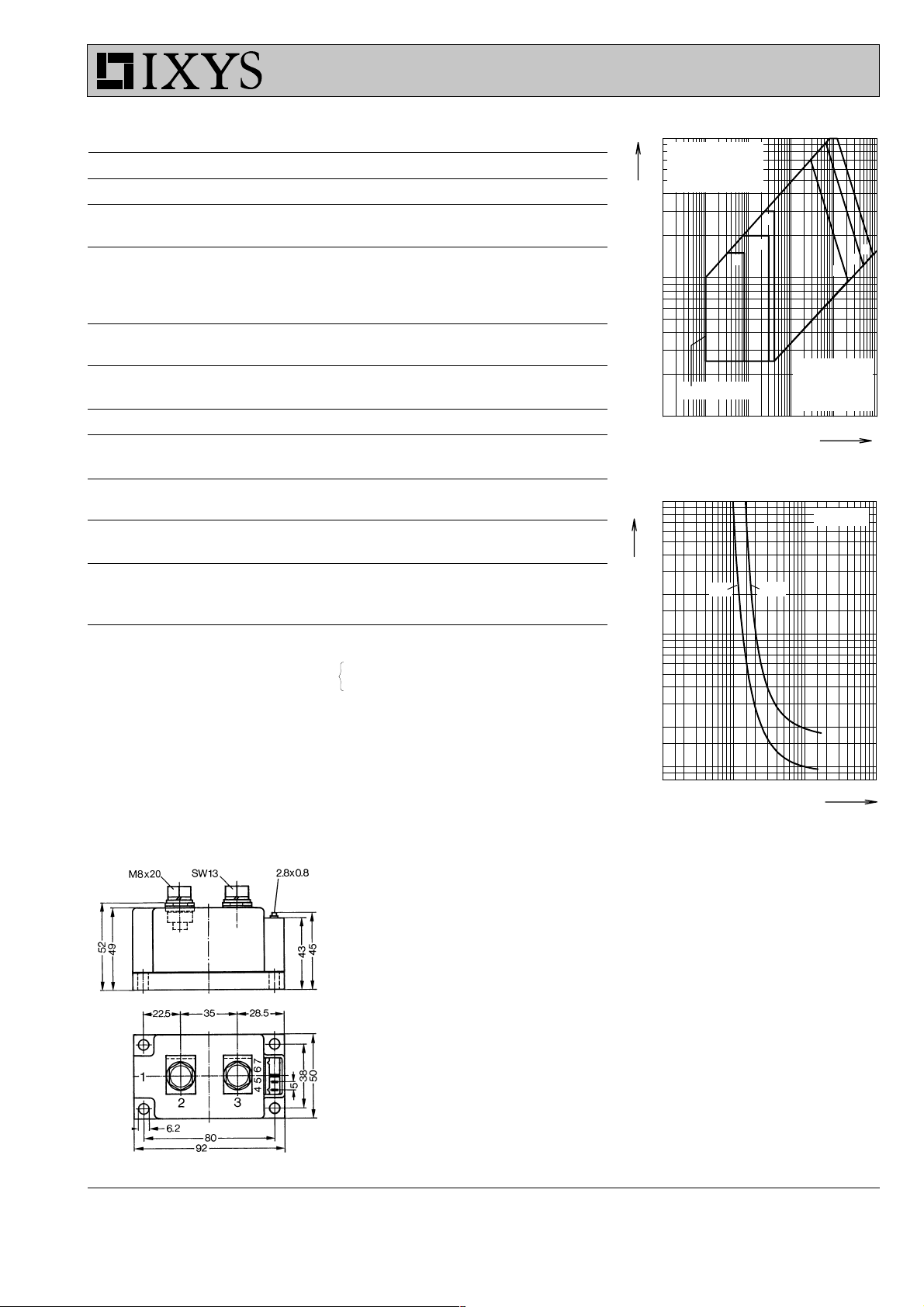
Mounting torque (M6) Nm/lb.in.
tP = 30 msW
tP = 500 msW
Terminal connection torque (M8) Nm/lb.in.
Weight Typical including screws g
3542
750
A
464
15000
16000
13000
14400
1125000
1062000
845000
813000
A/ms
1000
V/ms
120
60
30
10
-40...130
130
-40...125
W
V
°C
°C
°C
3000
3600
4.5-7/40-62
11-13/97-115
650
I
TRMS
I
TAV
V
= 750 A
= 464 A
= 2000-2200 V
RRM
2
3
5
4
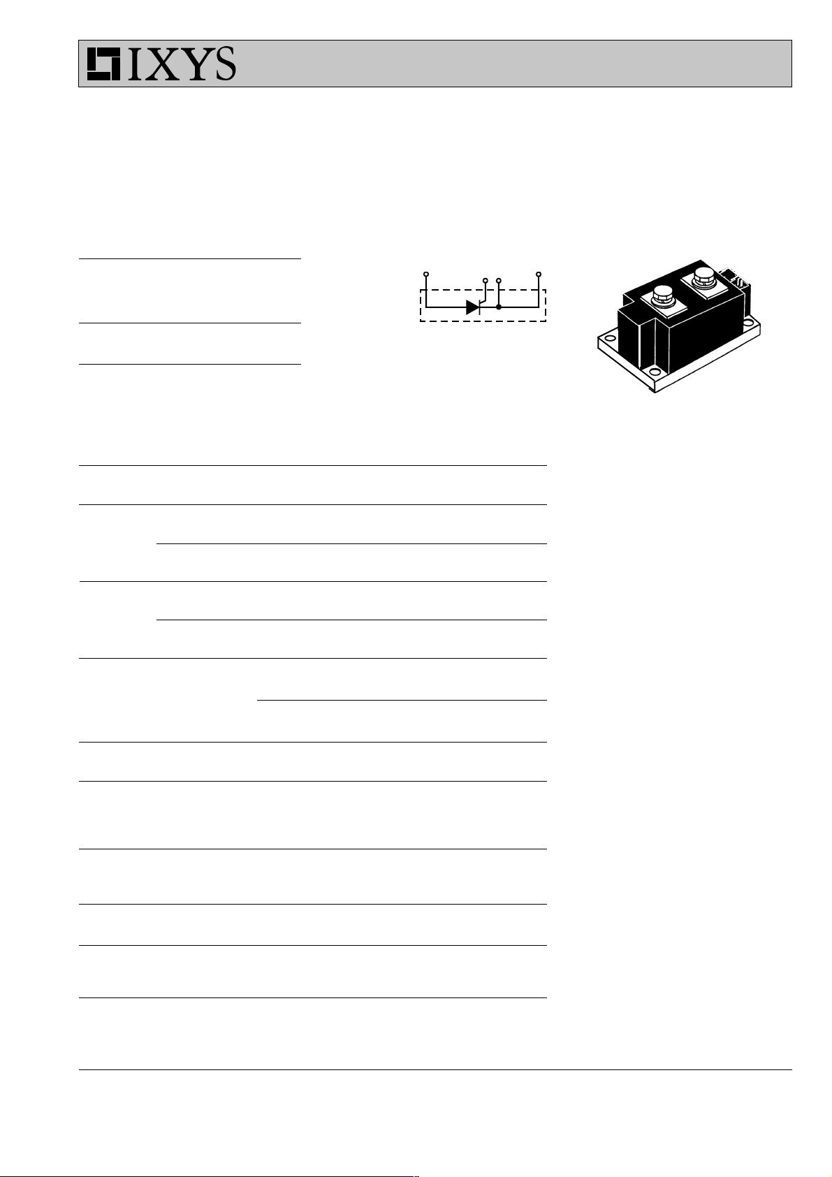
Features
●
Direct copper bonded Al2O3 -ceramic
with copper base plate
●
Planar passivated chips
●
Isolation voltage 3600 V~
●
UL applied
●
Keyed gate/cathode twin pins
Applications
●
Motor control, soft starter
●
Power converter
●
Heat and temperature control for
industrial furnaces and chemical
processes
●
Lighting control
●
Solid state switches
Advantages
●
Improved temperature and power
cycling
●
Reduced protection circuits
Data according to IEC 60747 refer to a single thyristor/diode unless otherwise stated.
IXYS reserves the right to change limits, test conditions and dimensions
© 2000 IXYS All rights reserved
030
1 - 4
Page 2
MCO 450
Symbol Test Conditions Characteristic Values
I
RRM
V
T
V
T0
r
T
V
GT
I
GT
V
GD
I
GD
I
L
1
I
H
t
gd
TVJ= T
IT=A; T
For power-loss calculations only (TVJ = T
VD= 6 V; TVJ = 25°CV
VD= 6 V; TVJ = 25°CmA
TVJ= T
TVJ= T
TVJ = 25°C; VD = 6 V; tP = msmA
diG/dt = A/ms; IG = 1 A
TVJ= 25°C; VD = 6 V; RGK = ¥ mA
TVJ= 25°C; VD = 1/2 V
diG/dt = A/ms; IG = A
t
q
TVJ = T
dv/dt = V/ms; IT = A; -di/dt = A/ms
R
thJC
R
thJK
d
S
d
A
DC current K/W
DC current K/W
Creep distance on surface mm
Strike distance in air mm
a Maximum allowable acceleration m/s
Optional accessories for modules
Keyed Gate/Cathode twin plugs with wire length = 350 mm, gate = yellow, cathode = red
Type ZY 180 L (L = Left for pin pair 4/5)
; VR = V
VJM
600 1.15
RRM
= 25°CV
VJ
)V
VJM
40
0.77
0.42
mA
mW
2
TVJ = -40°CV
3
300
TVJ = -40°CmA
;VD = 2/3 V
VJM
;VD = 2/3 V
VJM
DRM
DRM
400
0.25
10
V
mA
30 400
300
ms
DRM
2
11
; VR = 100 V; VD = 2/3 V
VJM
; tP = 200 ms typ. ms
DRM
350
50 500 10
0.072
0.096
12.7
9.6
50
UL 758, style 1385, File E 38136,
CSA class 5851, guide 460-1-1, appl. 41234
10
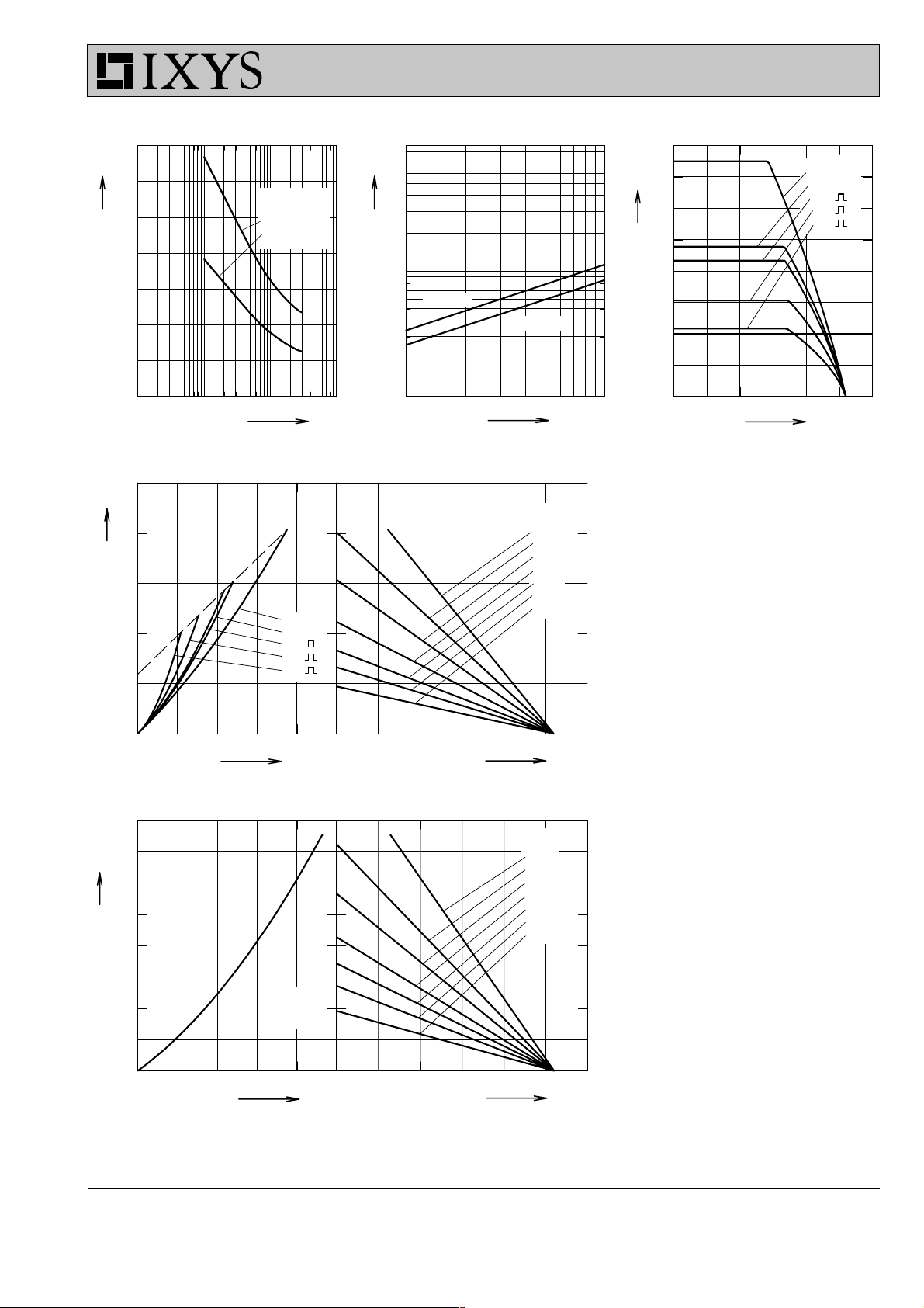
1: IGT, T
= 130°C
VJ
, T
= 25°C
2: I
GT
-3
3: I
IGD, T
VJ
, T
= -40°C
GT
VJ
3
2
1
= 130°C
VJ
-2
10
-1
10
V
V
G
1
0.1
10
Fig. 1 Gate trigger characteristics
100
µs
t
gd
typ.
2
10
Limit
6
5
4
4: P
= 20 W
GM
= 60 W
5: P
GM
= 120 W
6: P
GM
0
1
10
10
I
G
T
VJ
A
= 25°C
2
10
Dimensions in mm (1 mm = 0.0394")
© 2000 IXYS All rights reserved
1
0.01 0.1 1 10
I
G
Fig. 2 Gate trigger delay time
A
2 - 4
Page 3
MCO 450
14000
I
TSM
12000
A
10000
8000
6000
4000
2000
0
0.001 0.01 0.1 1
Fig. 3 Surge overload current
: Crest value, t: duration
I
TSM
1000
P
tot
W
800
600
400
200
50 Hz
80 % V
RRM
TVJ = 45°C
= 130°C
T
VJ
DC
180° sin
120°
60°
30°
7
10
VR = 0V
I2t
A2s
6
10
TVJ = 45°C
TVJ = 130°C
5
10
s
t
110
ms
t
800
A
700
I
TAVM
600
500
400
300
200
100
0
0 25 50 75 100 125 150
DC
180° sin
120°
60°
30°
T
C
°C
Fig. 4 I2t versus time (1-10 ms) Fig. 5 Maximum forward current
at case temperature
Fig. 6 Power dissipation versus on-
R
thKA
0.03
0.07
0.12
0.2
0.3
0.4
0.6
K/W
state current and ambient
temperature
0
0 200 400 600 800
4000
W
3500
P
tot
3000
2500
2000
1500
1000
500
0
0 300 600 900 1200
A
I
TAVM
Circuit
B6
6xMCO450
I
dAVM
0 25 50 75 100 125 150
R
thKA
0.01
0.02
0.03
0.045
0.06
0.08
0.12
0 25 50 75 100 125 150
A
T
A
K/W
T
°C
Fig. 7 Three phase rectifier bridge:
Power dissipation versus direct
output current and ambient
temperature
°C
A
© 2000 IXYS All rights reserved
3 - 4
Page 4

MCO 450
4000
W
3500
P
tot
3000
2500
2000
1500
10
-2
Circuit
W3
6xMCO450
A
0 25 50 75 100 125 150
I
RMS
30°
60°
120°
180°
DC
-1
10
0
10
1000
500
0
0 300 600 900
0.12
K/W
0.10
0.08
Z
thJC
0.06
0.04
0.02
0.00
-3
10
R
K/W
thKA
0.01
0.02
0.03
0.045
0.06
0.08
0.12
°C
T
A
1
10
s
t
Fig. 8 Three phase AC-controller:
Power dissipation versus RMS
output current and ambient
temperature
Fig. 9 Transient thermal impedance
junction to case
R
for various conduction angles d:
thJC
d R
thJC
DC 0.072
180° 0.0768
120° 0.081
60° 0.092
30° 0.111
calculation:
thJC
(K/W) ti (s)
thi
2
10
Constants for Z
iR
1 0.0035 0.0054
2 0.0186 0.098
3 0.0432 0.54
(K/W)
4 0.0067 12
0.14
K/W
0.12
Z
thJK
0.10
0.08
0.06
0.04
0.02
0.00
-3
10
-2
10
© 2000 IXYS All rights reserved
Fig.10Transient thermal impedance
junction to heatsink
R
for various conduction angles d:
thJK
d R
thJK
(K/W)
DC 0.096
180° 0.1
120° 0.105
30°
60°
120°
180°
DC
-1
10
0
10
1
10
s
t
2
10
60° 0.116
30° 0.135
Constants for Z
iR
calculation:
thJK
(K/W) ti (s)
thi
1 0.0035 0.0054
2 0.0186 0.098
3 0.0432 0.54
4 0.0067 12
5 0.024 12
4 - 4
 Loading...