

Page 1
MOTOROLA
SEMICONDUCTOR TECHNICAL DATA
Advance Information
Order this document
by MCM8A10/D
MCM8A10
1M x 8 Bit
Fast Static RAM Module
The MCM8A10 is an 8M bit static random access memory module organized
as 1,048,576 words of 8 bits. The module is offered in a 72–lead single in–line
memory module (SIMM). Eight MCM6227B fast static RAMs, packaged in
28–lead SOJ packages are mounted on a printed circuit board along with eight
decoupling capacitors.
The MCM6227B is organized as 1,048,576 words of 1 bit. Static design eliminates the need for external clocks or timing strobes, while CMOS circuitry reduces power consumption and provides for greater reliability .
The MCM8A10 is equipped with a chip enable (E
enable (W0
– W7) inputs, allowing for greater system flexibility .
• Single 5 V ± 5% Power Supply
• Fast Access Times: 15 ns
• Three–State Outputs
• Fully TTL Compatible
• High Board Density SIMM Package
• Bit Operation: Eight Separate Write Enables, One for Each Bit
• High Quality Six–Layer FR4 PWB with Separate Internal Power and
Ground Planes
) and eight separate write
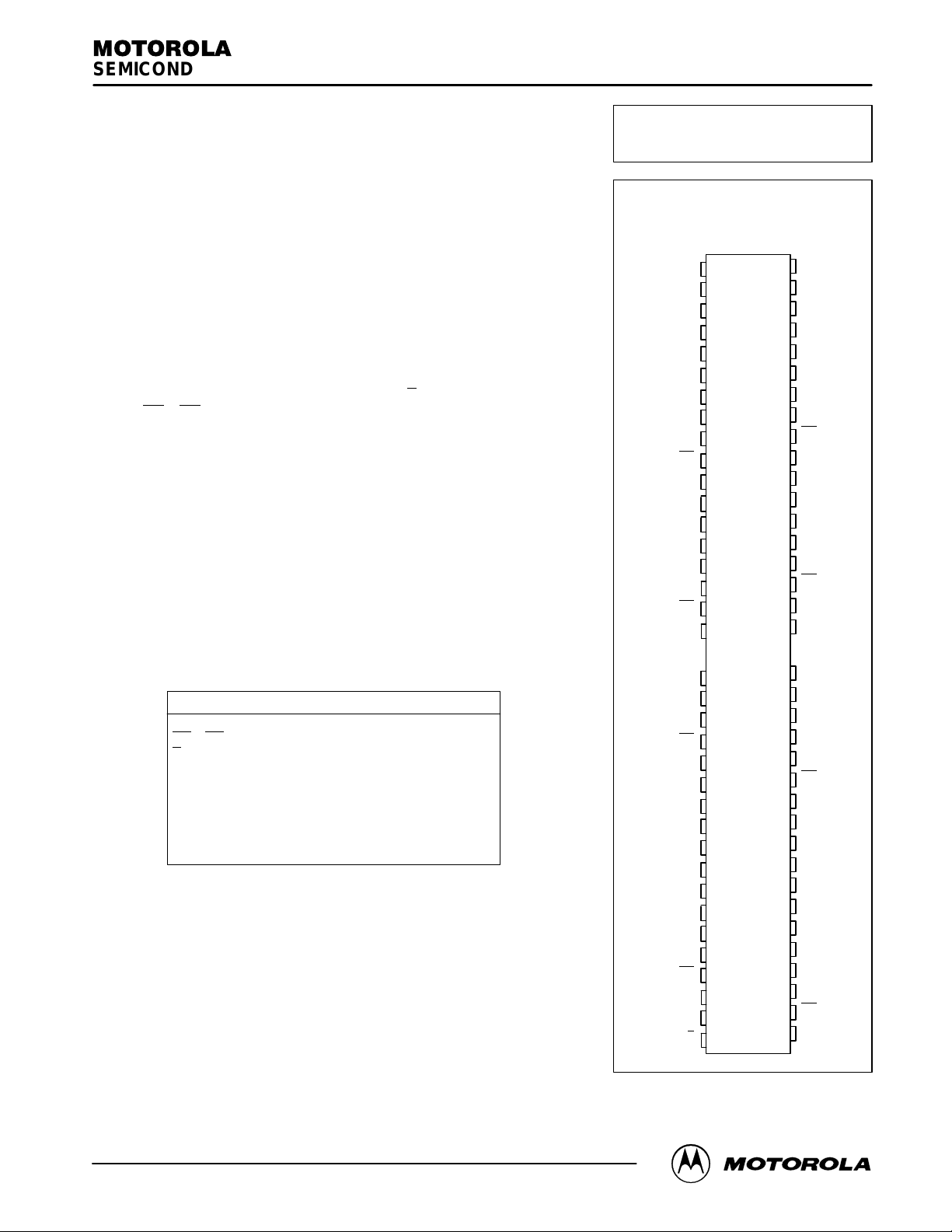
PIN ASSIGNMENT
TOP VIEW
72-LEAD SIMM – CASE TBD
A0
11
13
15
17
19
21
23
25
27
29
31
33
35
1
3
5
7
9
A2
V
CC
A4
A6
V
SS
A8
Q0
W0
V
CC
D1
A10
V
SS
DAISY
Q2
W2
V
CC
D3
A1
V
SS
A3
A5
A7
V
CC
A9
D0
V
SS
W1
Q1
A11
V
CC
DAISY
D2
V
SS
W3
Q3
2
4
6
8
10
12
14
16
18
20
22
24
26
28
30
32
34
36
PD1 38
V
PIN NAMES
A0 – A19 Address Inputs. . . . . . . . . . . . . . . . . . . . . . . . . . . . .
W0
– W7 Write Enables. . . . . . . . . . . . . . . . . . . . . . . . . . . . . .
E
D0 – D7 Data Inputs. . . . . . . . . . . . . . . . . . . . . . . . . . . . . . . . .
Q0 – Q7 Data Outputs. . . . . . . . . . . . . . . . . . . . . . . . . . . . . . .
PD0 – PD2 Package Density. . . . . . . . . . . . . . . . . . . . . . . . .
DAISY Pins Single Net. . . . . . . . . . . . . . . . . . . . . . . . . . . . . .
V
CC
V
SS
For proper operation of the device, VSS must be connected
to ground.
This document contains information on a new product. Specifications and information herein are subject to change without notice.
Chip Enable. . . . . . . . . . . . . . . . . . . . . . . . . . . . . . . . . . . . . .
+ 5 V Power Supply. . . . . . . . . . . . . . . . . . . . . . . . . . . .
Ground. . . . . . . . . . . . . . . . . . . . . . . . . . . . . . . . . . . . . . .
CC
Q4
W4
V
CC
D5
A21
A19
V
CC
A17
A15
V
SS
A13
Q6
W6
V
CC
D7E70
40
42
44
46
48
50
52
54
56
58
60
62
64
66
68
72
37
39
41
43
45
47
49
51
53
55
57
59
61
63
65
67
69
71
PD0
V
SS
PD2
D4
V
SS
W5
Q5
A20
V
SS
A18
A16
A14
V
CC
A12
D6
V
SS
W7
Q7
10/30/96
Motorola, Inc. 1996
MOTOROLA FAST SRAM
MCM8A10
1
Page 2
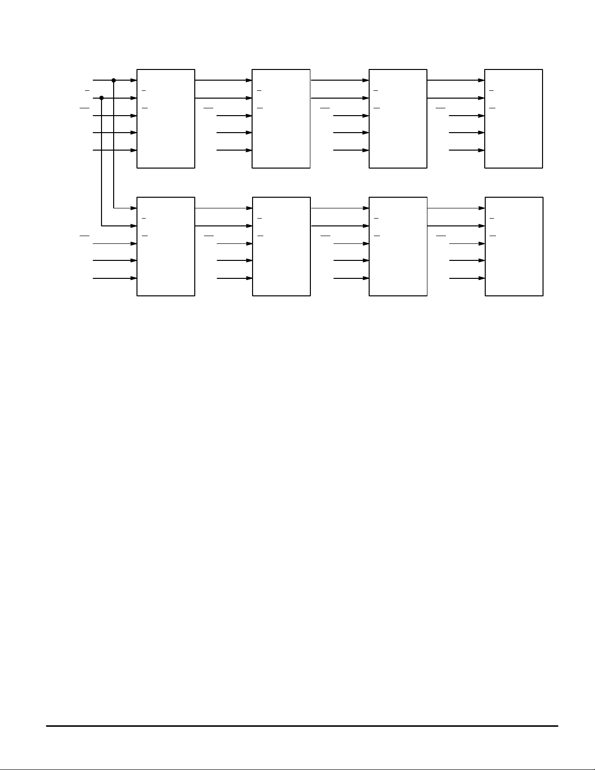
FUNCTIONAL BLOCK DIAGRAM
1M x 8 MEMORY MODULE
A0 – A19
E
W0
D0
Q0
D4
Q4
PD0 — Open
PD1 — V
PD2 — Open
SS
A0 – A19
E
W
D
Q
1M x 1
A0 – A19
E
WW4
D
Q
1M x 1
D1
Q1
D5
Q5
A0 – A19
E
WW1
D
Q
1M x 1
A0 – A19
E
WW5
D
Q
1M x 1
D2
Q2
D6
Q6
A0 – A19
E
WW2
D
Q
1M x 1
A0 – A19
E
WW6
D
Q
1M x 1
D3
Q3
D7
Q7
A0 – A19
E
WW3
D
Q
1M x 1
A0 – A19
E
WW7
D
Q
1M x 1
MCM8A10
2
MOTOROLA FAST SRAM
Page 3
TRUTH TABLE
E W Mode I/O Pin Cycle Current
H X Not Selected High–Z — I
L H Read D
L L Write High–Z Write I
NOTE: H = High, L = Low, X = Don’t Care
out
Read I
SB1
, I
CCA
CCA
SB2
ABSOLUTE MAXIMUM RATINGS (See Note)
Rating Symbol Value Unit
Power Supply Voltage Relative to V
Voltage Relative to VSS for Any Pin
Except V
Output Current I
Power Dissipation P
Temperature Under Bias T
Operating Temperature T
Storage Temperature T
NOTE: Permanent device damage may occur if ABSOLUTE MAXIMUM RATINGS are
CC
exceeded. Functional operation should be restricted to RECOMMENDED OPERATING CONDITIONS. Exposure to higher than recommended voltages for
extended periods of time could affect device reliability.
SS
V
CC
Vin, V
out
bias
stg
– 0.5 to 7.0 V
– 0.5 to VCC + 0.5 V
out
± 20
D
A
8.8 W
– 10 to + 85 °C
0 to + 70 °C
– 55 to + 150 °C
mA
This device contains circuitry to protect the
inputs against damage due to high static voltages or electric fields; however, it is advised
that normal precautions be taken to avoid
application of any voltage higher than maximum rated voltages to these high–impedance
circuits.
This CMOS memory circuit has been
designed to meet the dc and ac specifications
shown in the tables, after thermal equilibrium
has been established. The circuit is in a test
socket or mounted on a printed circuit board
and transverse air flow of at least 500 linear feet
per minute is maintained.
DC OPERA TING CONDITIONS AND CHARACTERISTICS
(VCC = 5.0 V ± 5%, TA = 0 to 70°C, Unless Otherwise Noted)
RECOMMENDED OPERATING CONDITIONS
Parameter Symbol Min Max Unit
Supply Voltage (Operating Voltage Range) V
Input High Voltage V
Input Low Voltage V
*VIL (min) = – 0.5 V dc; VIL (min) = – 2.0 V ac (pulse width ≤ 20 ns).
**VIH (max) = VCC + 0.3 V dc; VIH (max) = VCC + 2 V ac (pulse width ≤ 20 ns).
DC CHARACTERISTICS AND SUPPLY CURRENTS
Parameter Symbol Min Max Unit
Input Leakage Current (All Inputs, Vin = 0 to VCC) I
Output Leakage Current (E = VIH, V
AC Active Supply Current (I
AC Standby Current (VCC = max, E = VIH, f ≤ f
CMOS Standby Current (E ≥ VCC – 0.2 V, Vin ≤ VSS + 0.2 V or ≥ VCC – 0.2 V,
VCC = max, f = 0 MHz)
Output Low Voltage (IOL = + 8.0 mA) V
Output High Voltage (IOH = – 4.0 mA) V
out
= 0 to VCC) I
out
= 0 mA, VCC = max) I
) I
max
CC
IH
IL
lkg(I)
lkg(O)
CCA
SB1
I
SB2
OL
OH
4.75 5.25 V
2.2 VCC +0.3** V
– 0.5* 0.8 V
— ± 1 µA
— ± 1 µA
— 920 mA
— 320 mA
— 40 mA
— 0.4 V
2.4 — V
CAPACITANCE (f = 1.0 MHz, dV = 3.0 V, T
Characteristic
Input Capacitance Address Inputs
Input and Output Capacitance D, Q Cin, C
= 25°C, Periodically Sampled Rather Than 100% Tested)
A
Symbol Typ Max Unit
E
W
MOTOROLA FAST SRAM
C
in
out
42
50
10
10 13 pF
58
74
13
pF
MCM8A10
3
Page 4

AC OPERA TING CONDITIONS AND CHARACTERISTICS
(VCC = 5.0 V ± 5%, TA = 0 to + 70°C, Unless Otherwise Noted)
Input Pulse Levels 0 to 3.0 V. . . . . . . . . . . . . . . . . . . . . . . . . . . . . . . . .
Input Rise/Fall Time 2 ns. . . . . . . . . . . . . . . . . . . . . . . . . . . . . . . . . . . .
Input Timing Measurement Reference Level 1.5 V. . . . . . . . . . . . . . .
Output Timing Measurement Reference Level 1.5 V. . . . . . . . . . . . .
Output Load See Figure 1a. . . . . . . . . . . . . . . . . . . . . . . . . . . . . . . . . .
READ CYCLE TIMING (See Notes 1 and 2)
MCM8A10–15
Parameter Symbol
Read Cycle Time t
Address Access Time t
Enable Access Time t
Output Hold from Address Change t
Enable Low to Output Active t
Enable High to Output High–Z t
NOTES:
1. W
is high for read cycle.
2. Product sensitivities to noise require proper grounding and decoupling of power supplies as well as minimization or elimination of bus
contention conditions during read and write cycles.
3. All timings are referenced from the last valid address to the first transitioning address.
4. Addresses valid prior to or coincident with E
5. At any given voltage and temperature, t
6. Transition is measured ± 500 mV from steady–state voltage with load of Figure 1b.
7. This parameter is sampled and not 100% tested.
8. Device is continuously selected (E
≤ VIL).
going low.
max is less than t
EHQZ
min, both for a given device and from device to device.
ELQX
AVAV
AVQV
ELQV
AXQX
ELQX
EHQZ
Min Max
15 — ns 2, 3
— 15 ns
— 15 ns 4
5 — ns
5 — ns 5, 6, 7
0 6 ns 5, 6, 7
Unit Notes
OUTPUT
RL = 50
Ω
OUTPUT
Z0 = 50
Ω
VL = 1.5 V
255
(a) (b)
Figure 1. AC Test Loads
+ 5 V
480
Ω
Ω
5 pF
The table of timing values shows either a
minimum or a maximum limit for each parameter. Input requirements are specified from
the external system point of view. Thus, address setup time is shown as a minimum
since the system must supply at least that
much time. On the other hand, responses
from the memory are specified from the device point of view. Thus, the access time is
shown as a maximum since the device never
provides data later than that time.
TIMING LIMITS
MCM8A10
4
MOTOROLA FAST SRAM
Page 5

A (ADDRESS)
READ CYCLE 1 (See Notes 1, 2, and 8)
t
AVAV
t
AXQX
Q (DATA OUT)
A (ADDRESS)
E
(CHIP ENABLE)
Q (DATA OUT)
I
SUPPLY CURRENT
CC
I
SB
HIGH–Z
t
AVQV
READ CYCLE 2 (See Note 4)
t
AVAV
t
ELQV
t
ELQX
t
AVQV
t
ELICCH
DATA VALID
DATA VALIDPREVIOUS DATA VALID
t
EHQZ
t
EHICCL
MOTOROLA FAST SRAM
MCM8A10
5
Page 6

WRITE CYCLE 1 (W Controlled, See Notes 1 and 2)
MCM8A10–15
Parameter Symbol
Write Cycle Time t
Address Setup Time t
Address Valid to End of W rite t
Write Pulse Width t
Data Valid to End of W rite t
Data Hold TIme t
Write Low to Data High–Z t
Write High to Output Active t
Write Recovery Time t
NOTES:
1. A write occurs during the overlap of E
2. Product sensitivities to noise require proper grounding and decoupling of power supplies as well as minimization or elimination of bus
contention conditions during read and write cycles.
3. All timings are referenced from the last valid address to the first transitioning address.
4. Transition is measured ± 500 mV from steady–state voltage with load of Figure 1b.
5. This parameter is sampled and not 100% tested.
6. At any given voltage and temperature, t
low and W low.
max is less than t
WLQZ
min both for a given device and from device to device.
WHQX
AVAV
AVWL
AVWH
WLWH,
t
WLEH
DVWH
WHDX
WLQZ
WHQX
WHAX
Min Max
15 — ns 3
0 — ns
12 — ns
12 — ns
7 — ns
0 — ns
0 6 ns 4, 5, 6
5 — ns 4, 5, 6
0 — ns
Unit Notes
A (ADDRESS)
(CHIP ENABLE)
E
W
(WRITE ENABLE)
D (DATA IN)
Q (DATA OUT)
WRITE CYCLE 1 (W Controlled See Notes 1 and 2)
t
AVAV
t
AVWH
t
WLWH
t
WLEH
t
AVWL
t
WLQZ
HIGH–Z HIGH–Z
t
DVWH
DATA VALID
t
WHAX
t
WHDX
t
WHQX
MCM8A10
6
MOTOROLA FAST SRAM
Page 7

WRITE CYCLE 2 (E Controlled, See Notes 1 and 2)
MCM8A10–15
Parameter Symbol
Write Cycle Time t
Address Setup Time t
Address Valid to End of W rite t
Enable to End of Write t
Write Pulse Width t
Data Valid to End of W rite t
Data Hold Time t
Write Recovery Time t
NOTES:
1. A write occurs during the overlap of E
2. Product sensitivities to noise require proper grounding and decoupling of power supplies as well as minimization or elimination of bus
contention conditions during read and write cycles.
3. All timings are referenced from the last valid address to the first transitioning address.
4. If E
goes low coincident with or after W goes low, the output will remain in a high–impedance state.
5. If E
goes high coincident with or before W goes high, the output will remain in a high–impedance state.
low and W low.
AVAV
AVEL
AVEH
ELEH,
t
ELWH
WLEH
DVEH
EHDX
EHAX
Min Max
15 — ns 3
0 — ns
12 — ns
10 — ns 4, 5
12 — ns
7 — ns
0 — ns
0 — ns
Unit Notes
WRITE CYCLE 2 (E Controlled See Notes 1 and 2)
A (ADDRESS)
E
(CHIP ENABLE)
W (WRITE ENABLE)
D (DATA IN)
Q (DATA OUT)
t
AVEH
t
AVEL
HIGH–Z
ORDERING INFORMATION
(Order by Full Part Number)
MCM 8A10 XX XX
t
AVAV
t
WLEH
t
ELEH
t
ELWH
t
DVEH
DATA VALID
t
EHDX
t
EHAX
Part Number
MOTOROLA FAST SRAM
Speed (15 = 15 ns)Motorola Memory Prefix
Package (SG = Gold Pad SIMM)
Full Part Number — MCM8A10SG15
MCM8A10
7
Page 8

P ACKAGE DIMENSIONS
72–LEAD SIMM
CASE TBD
Motorola reserves the right to make changes without further notice to any products herein. Motorola makes no warranty , representation or guarantee regarding
the suitability of its products for any particular purpose, nor does Motorola assume any liability arising out of the application or use of any product or circuit, and
specifically disclaims any and all liability, including without limitation consequential or incidental damages. “T ypical” parameters which may be provided in Motorola
data sheets and/or specifications can and do vary in different applications and actual performance may vary over time. All operating parameters, including “Typicals”
must be validated for each customer application by customer’s technical experts. Motorola does not convey any license under its patent rights nor the rights of
others. Motorola products are not designed, intended, or authorized for use as components in systems intended for surgical implant into the body, or other
applications intended to support or sustain life, or for any other application in which the failure of the Motorola product could create a situation where personal injury
or death may occur. Should Buyer purchase or use Motorola products for any such unintended or unauthorized application, Buyer shall indemnify and hold Motorola
and its officers, employees, subsidiaries, affiliates, and distributors harmless against all claims, costs, damages, and expenses, and reasonable attorney fees
arising out of, directly or indirectly, any claim of personal injury or death associated with such unintended or unauthorized use, even if such claim alleges that
Motorola was negligent regarding the design or manufacture of the part. Motorola and are registered trademarks of Motorola, Inc. Motorola, Inc. is an Equal
Opportunity/Affirmative Action Employer.
How to reach us:
USA/EUROPE/ Locations Not Listed: Motorola Literature Distribution; JAP AN: Nippon Motorola Ltd.; Tatsumi–SPD–JLDC, 6F Seibu–Butsuryu–Center,
P.O. Box 5405; Denver, Colorado 80217. 1–800–441–2447 3–14–2 Tatsumi Koto–Ku, Tokyo 135, Japan. 81–3–3521–8315
Mfax: RMFAX0@email.sps.mot.com – TOUCHTONE 602–244–6609 ASIA/PACIFIC: Motorola Semiconductors H.K. Ltd.; 8B Tai Ping Industrial Park,
INTERNET: http://Design–NET.com 51 Ting Kok Road, Tai Po, N.T., Hong Kong. 852–26629298
MCM8A10
8
◊
MOTOROLA FAST SRAM
*MCM8A10/D*
MCM8A10/D
 Loading...