

Page 1
MCM72CF32•MCM72CF64
1
MOTOROLA FAST SRAM
Advance Information
256KB and 512KB BurstRAM
Secondary Cache Module for
Pentium
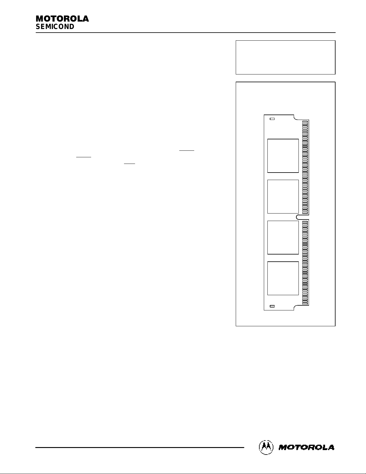
The MCM72CF32SG and MCM72CF64SG are designed to provide a burstable, high performance, 256K/512K L2 cache for the Pentium microprocessor.
The modules are configured as 32K x 72 and 64K x 72 bits in a 160 pin card edge
memory module. The module uses four of Motorola’s MCM67C518 or
MCM67C618 BiCMOS BurstRAMs.
Bursts can be initiated with either address status processor (ADSP
) or address
status controller (ADSC
). Subsequent burst addresses are generated internal to
the BurstRAM by the burst advance (ADV
) input pin.
Write cycles are internally self timed and are initiated by the rising edge of the
clock (K) input. Eight write enables are provided for byte write control.
The cache family is designed to interface with popular Pentium cache controllers with on board tag.
PD0 – PD2 are reserved for density identification.
• Pentium–style Burst Counter on Board
• Pipelined Data Out
• 160 Pin Card Edge Module
• Single 5 V ± 5% Power Supply
• All Inputs and Outputs are TTL Compatible
• Three State Outputs
• Byte Parity
• Byte Write Capability
• Fast Module Clock Rates: 66 MHz
• Decoupling Capacitors for each Fast Static RAM
• High Quality Multi–Layer FR4 PWB With Separate Power and Ground Planes
• I/Os are 3.3 V Compatible
• Burndy Connector, Part Number: CELP2X80SC3Z48
• Series 20Ω Resistors for Noise Immunity
BurstRAM is a trademark of Motorola.
Pentium is a trademark of Intel Corp.
This document contains information on a new product. Specifications and information herein are subject to change without notice.
160–LEAD CARD
EDGE
CASE 1113A–01
TOP VIEW
80
43
42
1
Order this document
by MCM72CF32/D
MOTOROLA
SEMICONDUCTOR TECHNICAL DATA
MCM72CF32
MCM72CF64
5/95
Motorola, Inc. 1995
Page 2
PIN ASSIGNMENT
68–LEAD CARD EDGE MODULE
TOP VIEW
V
SS
DQ63
VCC5
DQ61
VCC5
DQ59
DQ57
V
SS
DQP7
DQ55
DQ53
DQ51
V
SS
DQ49
DQ47
DQ45
DQ43
V
SS
DQ41
DQP5
DQ39
DQ37
DQ35
V
SS
DQ33
DQ31
DQ29
DQ27
DQ25
V
SS
DQP3
DQ23
DQ21
VCC5
DQ19
V
SS
DQ17
VCC5
DQ15
DQ13
V
SS
DQ11
81
82
83
84
85
86
87
88
89
90
91
92
93
94
95
96
97
98
99
100
101
102
103
104
105
106
107
108
109
110
111
112
113
114
115
116
117
118
119
120
121
122
1
2
3
4
5
6
7
8
9
10
11
12
13
14
15
16
17
18
19
20
21
22
23
24
25
26
27
28
29
30
31
32
33
34
35
36
37
38
39
40
41
42
V
SS
DQ62
VCC3*
DQ60
VCC3*
DQ58
DQ56
V
SS
DQP6
DQ54
DQ52
DQ50
V
SS
DQ48
DQ46
DQ44
DQ42
V
SS
DQ40
DQP4
DQ38
DQ36
DQ34
V
SS
DQ32
DQ30
DQ28
DQ26
DQ24
V
SS
DQP2
DQ22
DQ20
VCC3*
DQ18
V
SS
DQ16
VCC3*
DQ14
DQ12
V
SS
DQ10
43
44
45
46
47
48
49
50
51
52
53
54
55
56
57
58
59
60
61
62
63
64
65
66
67
68
69
70
71
72
73
74
75
76
77
78
79
80
123
124
125
126
127
128
129
130
131
132
133
134
135
136
137
138
139
140
141
142
143
144
145
146
147
148
149
150
151
152
153
154
155
156
157
158
159
160
VCC5
DQ9
DQP1
VCC5
DQ7
DQ5
DQ3
DQ1
V
SS
A3B
A4B
A5B
A6B
A7
V
SS
A9
A11
A13
A15
A17
V
SS
*A19
PD1
K0
*K2
V
SS
WE7
WE5
WE3
WE1
V
SS
ADSC1
E1
ADV1
G1
VCC5
ADSP1
V
SS
VCC3*
DQ8
DQP0
VCC3*
DQ6
DQ4
DQ2
DQ0
V
SS
A3A
A4A
A5A
A6A
A8
V
SS
A10
A12
A14
A16
A18**
V
SS
PD0
PD2
K1
K3*
V
SS
WE6
WE4
WE2
WE0
V
SS
ADSC0
E0
ADV0
G0
VCC3*
ADSP0
V
SS
PIN NAMES
A3 – A18 Address Inputs. . . . . . . . . . . . . . . . . . . . . .
K0, K1 Clock. . . . . . . . . . . . . . . . . . . . . . . . . . . . . . . .
W0
– W7 Byte Write. . . . . . . . . . . . . . . . . . . . . . . . . .
E0
, E1 Module Enable. . . . . . . . . . . . . . . . . . . . . . . .
G0
, G1 Module Output Enable. . . . . . . . . . . . . . . . .
DQ0 – DQ63 Cache Data Input/Output. . . . . . . . . .
DQP0 – DQP7 Data Parity Input/Output. . . . . . . . .
ADSC0
, ADSC1 Controller Address Status. . . . . .
ADSP0
, ADSP1 Processor Address Status. . . . . .
ADV0
, ADV1 Burst Advance. . . . . . . . . . . . . . . . . . .
PD0 – PD2 Presence Detect. . . . . . . . . . . . . . . . . .
VCC5 + 5 V Power Supply. . . . . . . . . . . . . . . . . . . . .
V
SS
Ground. . . . . . . . . . . . . . . . . . . . . . . . . . . . . . . .
* No Connect for MCM72CF32/MCM72CF64
** No Connect for MCM72CF32
MCM72CF32•MCM72CF64
2
MOTOROLA FAST SRAM
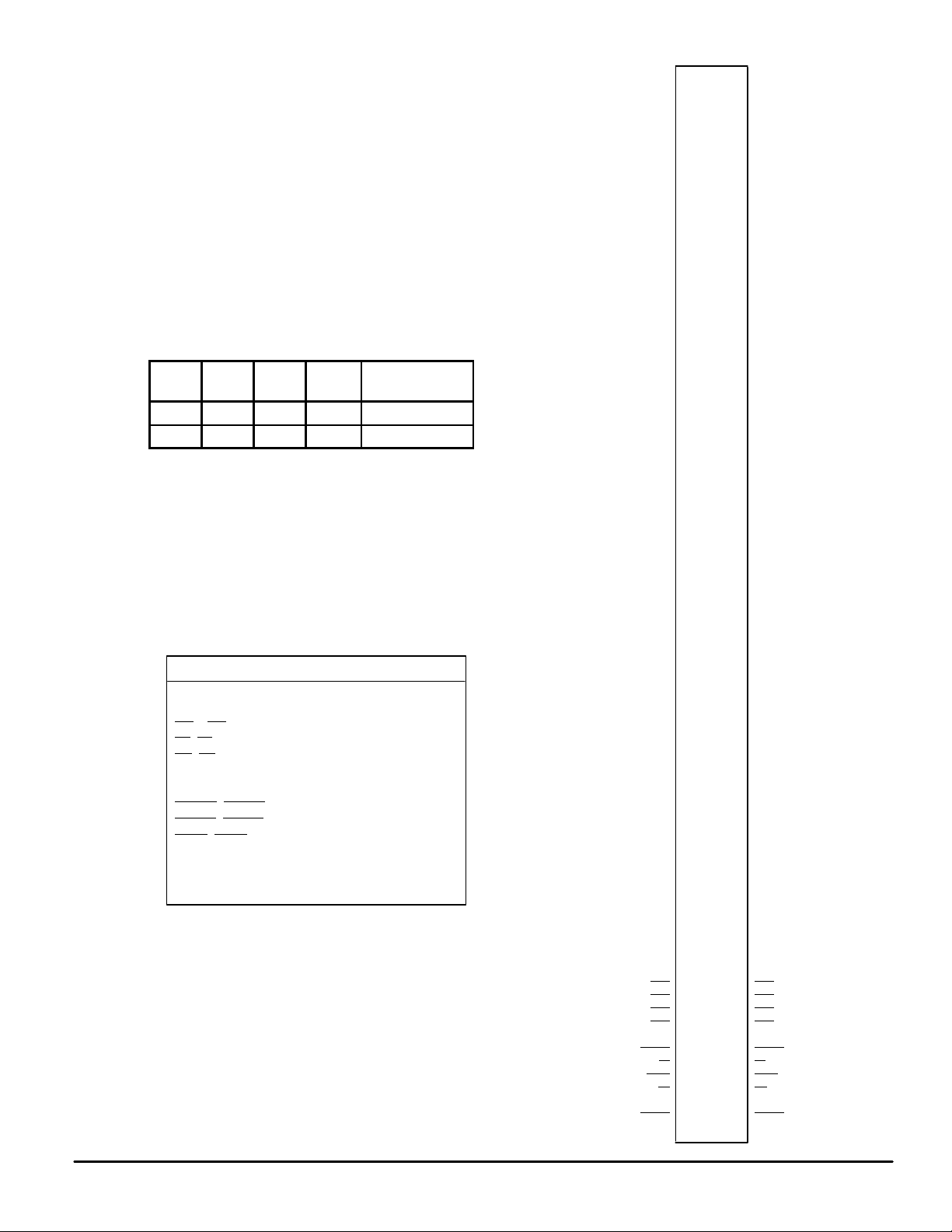
PD2 PD1 PD0
Cache
Size
Module
V
SS
V
SS
NC 256KB 72CF32SG
V
SS
V
SS
V
SS
512KB 72CF64SG
Page 3
MCM72CF32•MCM72CF64
3
MOTOROLA FAST SRAM
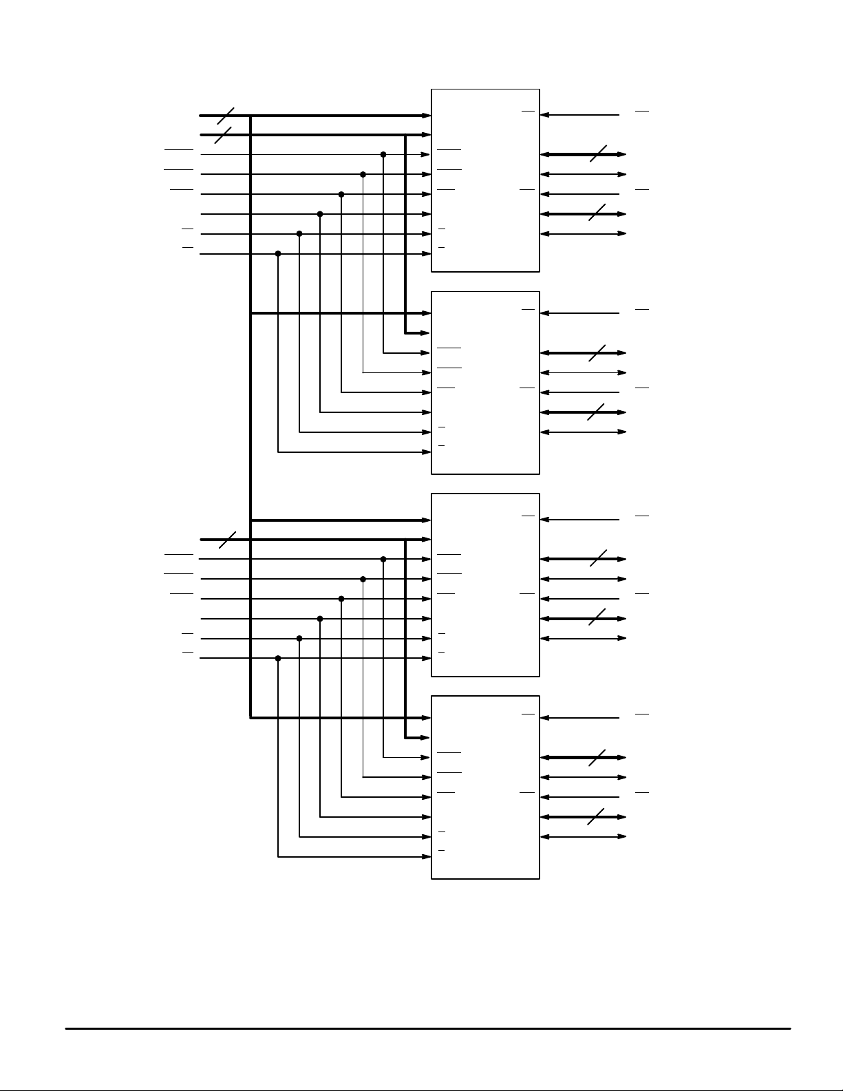
64K x 72 BurstRAM MEMORY MODULE BLOCK DIAGRAM
LW
MCM67C618
A4 – A15
ADV
K
G
E
DQ0 – DQ7
A7 – A18
E0
12
DQ8
UW
ADSP
ADSC
DQ9 – DQ16
DQ17
ADV0
ADSP0
ADSC0
K0
G0
DQ0 – DQ7
DQP0
DQ8 – DQ15
DQP1
W0
W1
8
8
LW
MCM67C618
A4 – A15
ADV
K
G
E
DQ0 – DQ7
DQ8
UW
ADSP
ADSC
DQ9 – DQ16
DQ17
DQ16 – DQ23
DQP2
DQ24 – DQ31
DQP3
W2
W3
8
8
A0 – A3A3A – A6A
A0 – A3
LW
MCM67C618
A4 – A15
ADV
K
G
E
DQ0 – DQ7
E1
DQ8
UW
ADSP
ADSC
DQ9 – DQ16
DQ17
ADV1
ADSP1
ADSC1
K1
G1
DQ32 – DQ39
DQP4
DQ40 – DQ47
DQP5
W4
W5
8
8
LW
MCM67C618
A4 – A15
ADV
K
G
E
DQ0 – DQ7
DQ8
UW
ADSP
ADSC
DQ9 – DQ16
DQ17
DQ48 – DQ55
DQP6
DQ56 – DQ63
DQP7
W6
W7
8
8
A0 – A3A3B – A6B
A0 – A3
4
4
DQ 0–63 and DQP 0–7 are series terminated with 20Ω resistors.
Page 4
MCM72CF32•MCM72CF64
4
MOTOROLA FAST SRAM
32K x 72 BurstRAM MEMORY MODULE BLOCK DIAGRAM
LW
MCM67C518
A4 – A14
ADV
K
G
E
DQ0 – DQ7
A7 – A17
E0
11
DQ8
UW
ADSP
ADSC
DQ9 – DQ16
DQ17
ADV0
ADSP0
ADSC0
K0
G0
DQ0 – DQ7
DQP0
DQ8 – DQ15
DQP1
W0
W1
8
8
LW
MCM67C518
A4 – A14
ADV
K
G
E
DQ0 – DQ7
DQ8
UW
ADSP
ADSC
DQ9 – DQ16
DQ17
DQ16 – DQ23
DQP2
DQ24 – DQ31
DQP3
W2
W3
8
8
A0 – A3A3A – A6A
A0 – A3
LW
MCM67C518
A4 – A14
ADV
K
G
E
DQ0 – DQ7
E1
DQ8
UW
ADSP
ADSC
DQ9 – DQ16
DQ17
ADV1
ADSP1
ADSC1
K1
G1
DQ32 – DQ39
DQP4
DQ40 – DQ47
DQP5
W4
W5
8
8
LW
MCM67C518
A4 – A14
ADV
K
G
E
DQ0 – DQ7
DQ8
UW
ADSP
ADSC
DQ9 – DQ16
DQ17
DQ48 – DQ55
DQP6
DQ56 – DQ63
DQP7
W6
W7
8
8
A0 – A3A3B – A6B
A0 – A3
4
A18 NC
4
DQ0–63 and DQP0–7 are series terminated with 20Ω resistors.
Page 5
MCM72CF32•MCM72CF64
5
MOTOROLA FAST SRAM
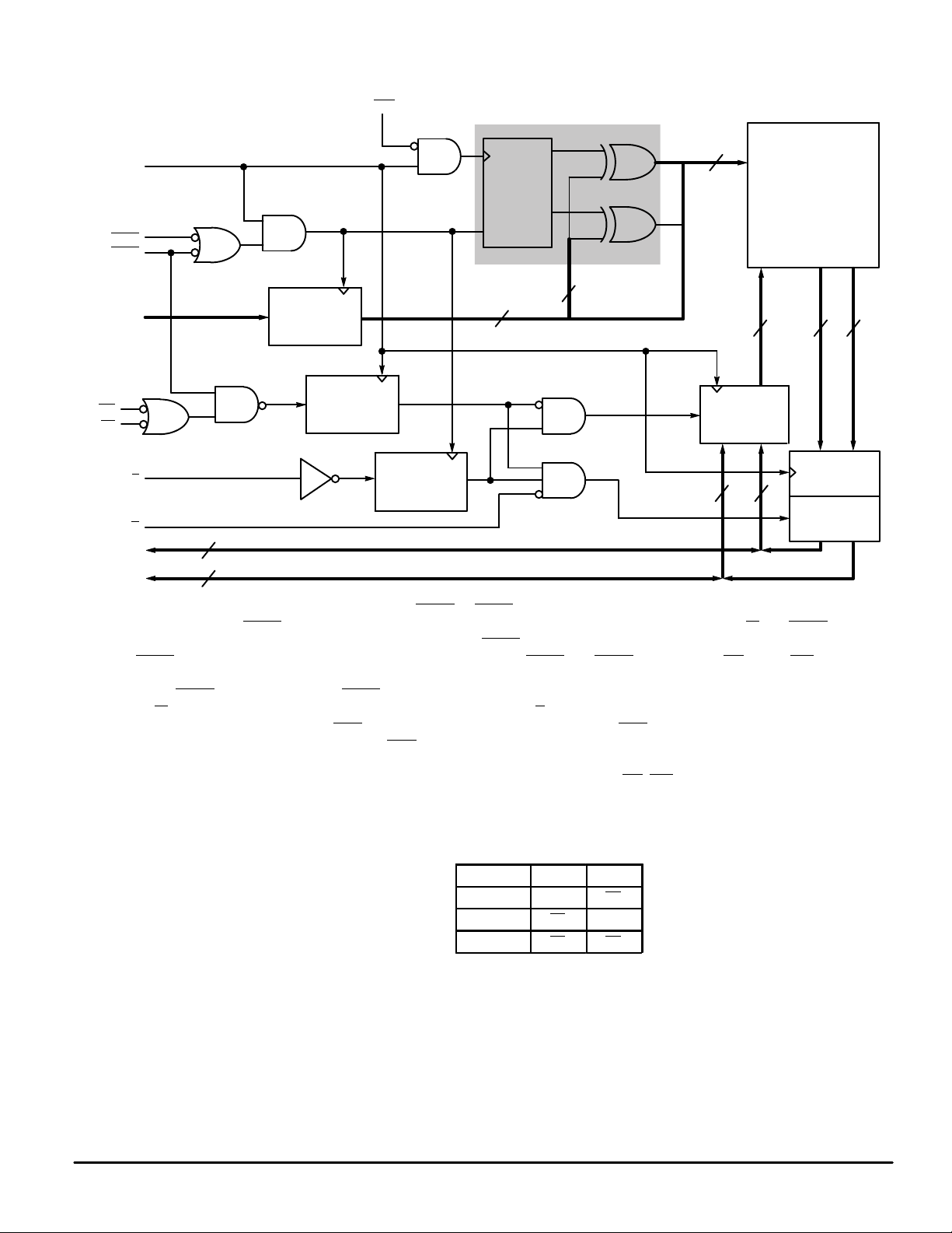
MCM67C618 BLOCK DIAGRAM (See Note)
BINARY
COUNTER
DQ0 – DQ8
CLR
Q0
Q1
A0
A1
K
ADSC
ADSP
A0 – A15
E
G
ADDRESS
REGISTER
WRITE
REGISTER
ENABLE
REGISTER
DATA–IN
REGISTERS
64K
×
18
MEMORY
ARRAY
ADV
BURST LOGIC
INTERNAL
ADDRESS
A0
′
A1
′
16
9
18
16
2
A2 – A15
A1 – A0
DQ9 – DQ17
9
9 9
9
9
UW
LW
OUTPUT
BUFFER
DATA–OUT
REGISTERS
NOTE: All registers are positive–edge triggered. The ADSC or ADSP signals control the duration of the burst and the start of the
next burst. When ADSP
is sampled low, any ongoing burst is interrupted and a read (independent of W and ADSC) is per-
formed using the new external address. Alternatively , an ADSP
–initiated two cycle WRITE can be performed by asserting
ADSP
and a valid address on the first cycle, then negating both ADSP and ADSC and asserting L W and/or UW with valid
data on the second cycle (see Single Write Cycle in WRITE CYCLES timing diagram).
When ADSC
is sampled low (and ADSP is sampled high), any ongoing burst is interrupted and a read or write (dependent
on W
) is performed using the new external address. Chip enable (E) is sampled only when a new base address is loaded.
After the first cycle of the burst, ADV
controls subsequent burst cycles. When ADV is sampled low, the internal address
is advanced prior to the operation. When ADV
is sampled high, the internal address is not advanced, thus inserting a wait
state into the burst sequence accesses. Upon completion of a burst, the address will wrap around to its initial state. See
BURST SEQUENCE TABLE. Write refers to either or both byte write enables (LW
, UW).
BURST SEQUENCE TABLE (See Note)
External Address A15 – A2 A1 A0
1st Burst Address A15 – A2 A1 A0
2nd Burst Address A15 – A2 A1 A0
3rd Burst Address A15 – A2 A1 A0
NOTE: The burst wraps around to its initial state upon completion.
Page 6

MCM72CF32•MCM72CF64
6
MOTOROLA FAST SRAM
SYNCHRONOUS TRUTH TABLE (See Notes 1, 2, and 3)
E
ADSP ADSC ADV UW or LW K Address Used Operation
H L X X X L–H N/A Deselected
H X L X X L–H N/A Deselected
L L X X X L–H External Address Read Cycle, Begin Burst
L H L X L L–H External Address Write Cycle, Begin Burst
L H L X H L–H External Address Read Cycle, Begin Burst
X H H L L L–H Next Address Write Cycle, Continue Burst
X H H L H L–H Next Address Read Cycle, Continue Burst
X H H H L L–H Current Address Write Cycle, Suspend Burst
X H H H H L–H Current Address Read Cycle, Suspend Burst
NOTES:
1. X means Don’t Care.
2. All inputs except G
must meet setup and hold times for the low–to–high transition of clock (K).
3. Wait states are inserted by suspending burst.
ASYNCHRONOUS TRUTH TABLE (See Notes 1 and 2)
Operation
G I/O Status
Read L Data Out
Read H High–Z
Write X High–Z — Data In
Deselected X High–Z
NOTES:
1. X means Don’t Care.
2. For a write operation following a read operation, G
must be high before the input data
required setup time and held high through the input data hold time.
ABSOLUTE MAXIMUM RATINGS (Voltages Referenced to V
SS
= 0 V)
Rating
Symbol Value Unit
Power Supply Voltage V
CC
– 0.5 to + 7.0 V
Voltage Relative to VSS for Any
Pin Except V
CC
Vin, V
out
– 0.5 to VCC + 0.5 V
Output Current (per I/O) I
out
± 30 mA
Power Dissipation P
D
6.4 W
Temperature Under Bias T
bias
– 10 to + 85 °C
Operating Temperature T
A
0 to +70 °C
Storage Temperature T
stg
– 55 to + 125 °C
NOTE: Permanent device damage may occur if ABSOLUTE MAXIMUM RATINGS are
exceeded. Functional operation should be restricted to RECOMMENDED OPERATING CONDITIONS. Exposure to higher than recommended voltages for
extended periods of time could affect device reliability.
ages or electric fields; however, it is advised
that normal precautions be taken to avoid
application of any voltage higher than maximum rated voltages to this high–impedance
circuit.
This device contains circuitry that will ensure
the output devices are in High–Z at power up.
This device contains circuitry to protect the
inputs against damage due to high static volt
Page 7

MCM72CF32•MCM72CF64
7
MOTOROLA FAST SRAM
DC OPERATING CONDITIONS AND CHARACTERISTICS
(VCC = 5.0 V ± 5%, TA = 0 to + 70°C, Unless Otherwise Noted)
RECOMMENDED OPERATING CONDITIONS
(Voltages referenced to VSS = 0 V)
Parameter
Symbol Min Max Unit
Supply Voltage (Operating Voltage Range) V
CC
4.75 5.25 V
Input High Voltage V
IH
2.2 VCC + 0.3
**
V
Input Low Voltage V
IL
– 0.5* 0.8 V
*VIL (min) = – 0.5 V dc; VIL (min) = – 2.0 V ac (pulse width ≤ 20.0 ns) for I ≤ 20.0 mA.
**VIH (max) = VCC + 0.3 V dc; VIH (max) = VCC + 2.0 V ac (pulse width ≤ 20.0 ns) for I ≤ 20.0 mA.
DC CHARACTERISTICS AND SUPPLY CURRENTS
Parameter Symbol Min Max Unit
Input Leakage Current (All Inputs, Vin = 0 to VCC) I
lkg(I)
— ± 1.0 µA
Output Leakage Current (G = VIH) I
lkg(O)
— ± 1.0 µA
AC Supply Current (G = VIH, E = VIL, I
out
= 0 mA, All Inputs = VIL or VIH,
VIL = 0.0 V and VIH ≥ 3.0 V, Cycle Time ≥ t
KHKH
min)
I
CCA66
— 1100 mA
AC Standby Current (E = VIH, I
out
= 0 mA, All Inputs = VIL and V
IH,
VIL = 0.0 V and VIH ≥ 3.0 V, Cycle Time ≥ t
KHKH
min)
I
SB1
— 300 mA
Output Low Voltage (IOL = + 8.0 mA) V
OL
— 0.4 V
Output High Voltage (IOH = – 4.0 mA) V
OH
2.4 3.3 V
NOTE: Good decoupling of the local power supply should always be used. DC characteristics are guaranteed for all possible Pentium bus cycles.
CAPACITANCE (f = 1.0 MHz, dV = 3.0 V, T
A
= 25°C, Periodically Sampled Rather Than 100% Tested)
Parameter
Symbol Max Unit
Input Capacitance (A7 – A18) C
in
20 pF
Input Capacitance (A3 – A6, ADSPx, ADSCx, ADVx, Kx, Gx, Ex, Wx) C
in
10 pF
Input/Output Capacitance (DQ0 – DQ63, DQP0 – DQP7) C
I/O
8 pF
Page 8

MCM72CF32•MCM72CF64
8
MOTOROLA FAST SRAM
AC OPERATING CONDITIONS AND CHARACTERISTICS
(VCC = 5.0 V ± 5%, TA = 0 to + 70°C, Unless Otherwise Noted)
Input Timing Measurement Reference Level 1.5 V. . . . . . . . . . . . . . .
Input Pulse Levels 0 to 3.0 V. . . . . . . . . . . . . . . . . . . . . . . . . . . . . . . . .
Input Rise/Fall Time 3 ns. . . . . . . . . . . . . . . . . . . . . . . . . . . . . . . . . . . .
Output Timing Reference Level 1.5 V. . . . . . . . . . . . . . . . . . . . . . . . . .
Output Load See Figure 1A Unless Otherwise Noted. . . . . . . . . . . .
READ/WRITE CYCLE TIMING (See Notes 1, 2, and 3)
MCM72CF64SG66
Parameter Symbol Min Max Unit Notes
Cycle Time t
KHKH
15 — ns
Clock Access Time t
KHQV
— 9 ns 5
Output Enable to Output Valid t
GLQV
— 6 ns
Clock High to Output Active t
KHQX1
2 — ns
Clock High to Output Change t
KHQX2
2 — ns
Output Enable to Output Active t
GLQX
1 — ns
Output Disable to Q High–Z t
GHQZ
2 6 ns 6
Clock High to Q High–Z t
KHQZ
— 6 ns
Clock High Pulse Width t
KHKL
5 — ns
Clock Low Pulse Width t
KLKH
5 — ns
Setup Times: Address
Address Status
Data In
Write
Address Advance
Chip Enable
t
AVKH
t
ADSVKH
t
DVKH
t
WVKH
t
ADVVKH
t
EVKH
2.5 — ns 7
Hold Times: Address
Address Status
Data In
Write
Address Advance
Chip Enable
t
KHAX
t
KHADSX
t
KHDX
t
KHWX
t
KHADVX
t
KHEX
0.5 — ns 7
NOTES:
1. In setup and hold time W (write) refers to either one or both byte write enables LW
and UW.
2. A read cycle is defined by UW
and LW high or ADSP low for the setup and hold times. A write cycle is defined by LW or UW low and ADSP
high for the setup and hold times.
3. All read and write cycle timings are referenced from K or G
.
4. G
is a don’t care when UW or LW is sampled low.
5. Maximum access times are guaranteed for all possible Pentium external bus cycles.
6. Transition is measured ± 500 mV from steady–state voltage with load of Figure 1B. This parameter is sampled rather than 100% tested. At
any given voltage and temperature, t
KHQZ
max is less than t
KHQZ1
min for a given device and from device to device.
7. This is a synchronous device. All addresses must meet the specified setup and hold times for
ALL
rising edges of K whenever ADSP or ADSC
is low, and the chip is selected. All other synchronous inputs must meet the specified setup and hold times for
ALL
rising edges of K when
the chip is enabled.Chip enable must be valid at each rising edge of clock for the device (when ADSP
or ADSC is low) to remain enabled.
AC TEST LOADS
Figure 1A Figure 1B
5 pF
+ 5 V
OUTPUT
480
Ω
255
Ω
OUTPUT
Z0 = 50
Ω
RL = 50
Ω
VL = 1.5 V
Page 9

MCM72CF32•MCM72CF64
9
MOTOROLA FAST SRAM
t
ADSVKH
t
KHADSX
t
KHKH
t
KHKL
t
KLKH
t
AVKH
t
KHAX
t
ADSVKH
t
KHADSX
t
WVKH
t
KHWX
t
ADVVKH
t
KHADVX
t
GLQV
t
GLQX
t
KHQV
t
KHQX2
t
EVKH
t
KHEX
t
KHQX1
t
KHQV
t
GHQZ
SINGLE READ
BURST READ
t
KHQZ
(BURST WRAPS AROUND
TO ITS INITIAL STATE)
A1 A2 A3 A4
(ADV SUSPENDS BURST)
ADSP STARTS NEW READ
A
K
ADSP
LW, UW
G
Q
ADV
E
ADSC
Q(A1) Q(A2) Q(A2 +1) Q(A2 + 2) Q(A2 + 3) Q(A2) Q(A2 +1) Q(A3)
CHIP
DESELECT
READ CYCLES
Page 10

MCM72CF32•MCM72CF64
10
MOTOROLA FAST SRAM
W IS IGNORED FOR FIRST CYCLE WHEN ADSP INITIATES BURST
NEW BURST WRITEBURST WRITE
ADV SUSPENDS BURST
t
KHDX
t
DVKH
t
KHADVX
t
ADVVKH
t
KHWX
t
WVKH
ADSC STARTS NEW BURST
A3
D(A3 + 2)D(A3 + 1)D(A3)D(A2 + 3)D(A2 + 2)D(A2 + 1)D(A2) D(A2 + 1)
t
KHADSX
t
ADSVKH
t
KHKH
t
KHKL
t
KLKH
D(A1)
t
KHADSX
t
ADSVKH
t
KHAX
t
AVKH
t
KHEX
t
EVKH
SINGLE WRITEBURST READ
t
GHQZ
K
ADSP
ADSC
ADDRESS
ADV
G
DATA IN
DATA OUT
A1 A2
E
LW, UW
WRITE CYCLES
Q(An – 1) Q(An)
(WITH A SUSPENDED CYCLE)
Page 11

MCM72CF32•MCM72CF64
11
MOTOROLA FAST SRAM
COMBINATION READ/WRITE CYCLES (E low, ADSC high)
t
ADVSKH
t
KHADSX
t
KHKH
t
KHKL
t
KLKH
t
AVKH
t
KHAX
t
KHWX
t
WVKH
t
ADVKH
t
KHQX1
t
KHQV
t
GHQZ
t
DVKH
t
KHDX
t
GLQX
t
KHQX2
Q(A1) Q(A3) Q(A3 + 1) Q(A3 + 2)
READ BURST READWRITE
D(A2)
A
K
ADSP
LW, UW
G
Q
ADV
D
t
KHADVX
A1 A2 A3
t
KHQV
Page 12

MCM72CF32•MCM72CF64
12
MOTOROLA FAST SRAM
APPLICATION EXAMPLE
512K Byte Burstable, Secondary Cache
Using MCM72CF64SG66 with a 66 MHz Pentium
DATA
ADDRESS
CLK
ADS
CONTROL
CACHE
CONTROL
LOGIC
ADV
ADSP
K0
ADSC
W
G0
DATA BUS
ADDRESS BUS
MCM67C618FN9
Pentium
CLOCK
ADDR ADDR DATA
K
Figure 2
MCM72CF64SG66
K1
G1
ORDERING INFORMATION
(Order by Full Part Number)
Motorola Memory Prefix
Part Number Package (SG = Gold Pad SIMM)
Speed (66 = 66 MHz)
MCM
72CF32
72CF64
XX XX
Full Part Numbers — MCM72CF32SG66
MCM72CF64SG66
Page 13

MCM72CF32•MCM72CF64
13
MOTOROLA FAST SRAM
PACKAGE DIMENSIONS
160–LEAD
CARD EDGE MODULE
CASE 1113A–01
É
É
É
É
É
É
É
É
É
É
É
É
É
É
É
É
M
P
(N)
A
SIDE VIEW
E
L
K
R
160X
H160X
R
W
D
160X
156X
Y
L
0.004 (0.1) X
S
T
DIM MIN MAX MIN MAX
MILLIMETERSINCHES
A 4.330 4.350 109.98 110.49
B 1.270 1.310 32.26 33.27
C ––– 0.454 ––– 11.53
D 0.033 0.037 0.84 0.94
E 2.265 2.275 57.53 57.79
F 0.075 BSC 1.91 BSC
G 0.050 BSC 1.27 BSC
H ––– 0.030 ––– 0.51
J 0.055 0.069 1.40 1.75
K 0.210 ––– 5.33 –––
L 1.955 1.965 49.66 49.91
M 2.155 2.165 54.74 54.99
N 0.110 REF 2.79 REF
P 0.125 ––– 3.18 –––
R 0.285 0.305 7.24 7.75
V 0.157 ––– 3.99 –––
W 0.040 0.060 1.02 1.52
AB ––– 0.262 ––– 6.66
AC 0.072 0.076 1.83 1.93
NOTES:
1. DIMENSIONING AND TOLERANCING PER ANSI
Y14.5M, 1982.
2. CONTROLLING DIMENSION: INCH.
3. CARD THICKNESS APPLIES ACROSS TABS AND
INCLUDES PLATING AND/OR METALLIZATION.
4. DIMENSIONS C AND V DEFINE A
DOUBLE–SIDED MODULE.
5. DIMENSION AB DEFINES OPTIONAL
SINGLE–SIDED MODULE.
6. STRAIGHTNESS CALLOUT APPLIES TO TAB
AREA ONLY.
G
É
É
É
É
É
É
É
É
É
2X
BACK VIEW
COMPONENT
VIEW AA
AC
F
–X–
–Y–
B
VIEW
AA
FULL R
COMPONENT
80 43 42 1
AREA
FRONT VIEW
V
NOTE 4
AB
NOTE 5
J NOTE 6
M
0.012 (0.3)
–T–
AREA
160 123 122 81
C
NOTE 4
Motorola reserves the right to make changes without further notice to any products herein. Motorola makes no warranty, representation or guarantee regarding
the suitability of its products for any particular purpose, nor does Motorola assume any liability arising out of the application or use of any product or circuit,
and specifically disclaims any and all liability, including without limitation consequential or incidental damages. “T ypical” parameters can and do vary in different
applications. All operating parameters, including “T ypicals” must be validated for each customer application by customer’s technical experts. Motorola does
not convey any license under its patent rights nor the rights of others. Motorola products are not designed, intended, or authorized for use as components in
systems intended for surgical implant into the body, or other applications intended to support or sustain life, or for any other application in which the failure of
the Motorola product could create a situation where personal injury or death may occur. Should Buyer purchase or use Motorola products for any such
unintended or unauthorized application, Buyer shall indemnify and hold Motorola and its officers, employees, subsidiaries, affiliates, and distributors harmless
against all claims, costs, damages, and expenses, and reasonable attorney fees arising out of, directly or indirectly, any claim of personal injury or death
associated with such unintended or unauthorized use, even if such claim alleges that Motorola was negligent regarding the design or manufacture of the part.
Motorola and are registered trademarks of Motorola, Inc. Motorola, Inc. is an Equal Opportunity/Affirmative Action Employer.
Page 14

MCM72CF32•MCM72CF64
14
MOTOROLA FAST SRAM
Literature Distribution Centers:
USA/EUROPE: Motorola Literature Distribution; P .O. Box 20912; Phoenix, Arizona 85036.
JAPAN: Nippon Motorola Ltd.; 4–32–1, Nishi–Gotanda, Shinagawa–ku, Tokyo 141, Japan.
ASIA PACIFIC: Motorola Semiconductors H.K. Ltd.; Silicon Harbour Center, No. 2 Dai King Street, Tai Po Industrial Estate, Tai Po, N.T., Hong Kong.
MCM72CF32/D
*MCM72CF32/D*
◊
 Loading...