

Datasheet MCM6946YJ12R, MCM6946YJ15, MCM6946YJ15R, MCM6946YJ8, MCM6946YJ8R Datasheet (Motorola)
...Page 1
MOTOROLA
SEMICONDUCTOR TECHNICAL DATA
Advance Information
512K x 8 Bit Static Random
Access Memory
Order this document
by MCM6946/D
MCM6946
The MCM6946 is a 4,194,304–bit static random access memory organized as
524,288 words of 8 bits. Static design eliminates the need for external clocks or
timing strobes.
The MCM6946 is equipped with chip enable (E
allowing for greater system flexibility and eliminating bus contention problems.
Either input, when high, will force the outputs into high–impedance.
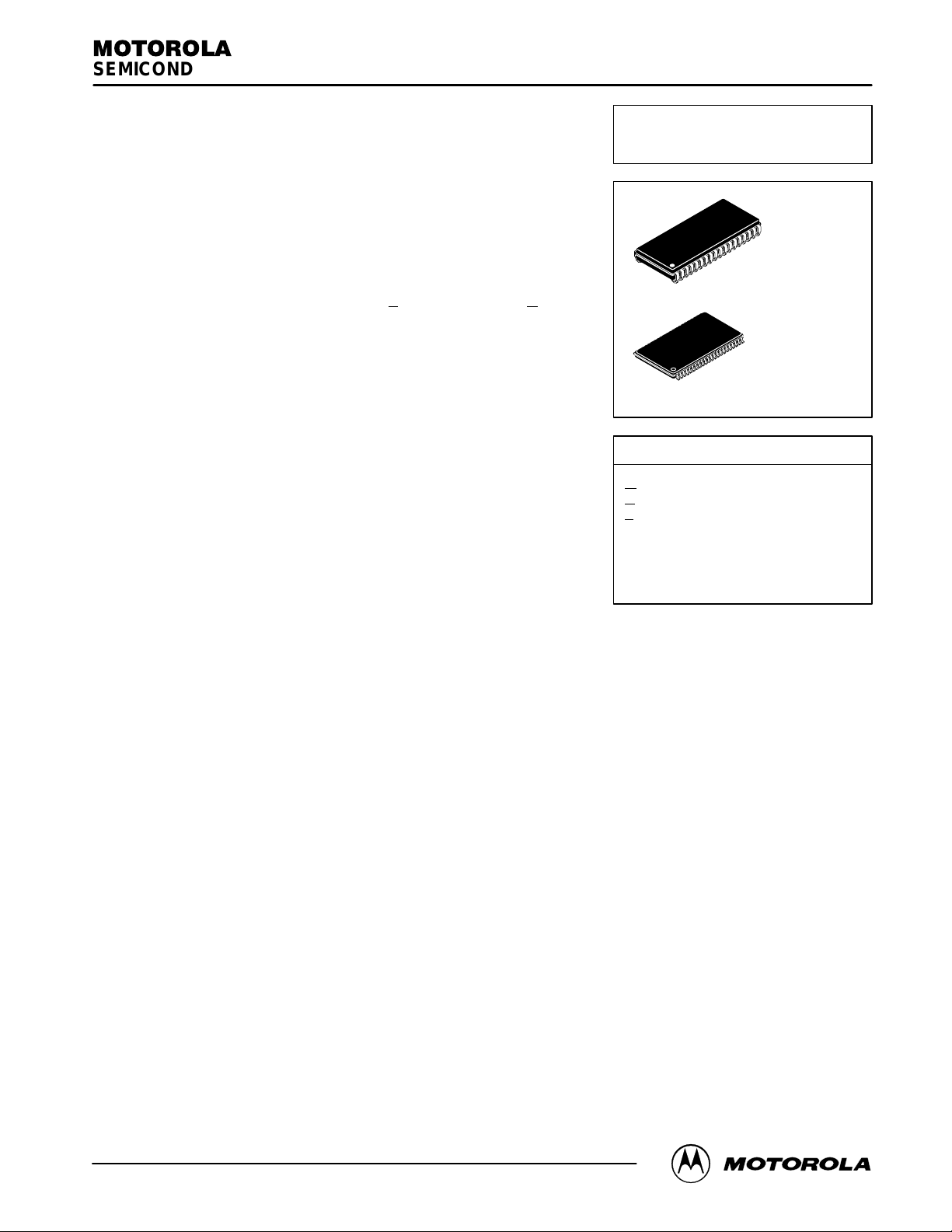
The MCM6946 is available in a 400 mil, 36–lead surface–mount SOJ package.
• Single 3.3 V – 5%, + 10% Power Supply
• Fast Access Time: 8/10/12/15 ns
• Equal Address and Chip Enable Access Time
• All Inputs and Outputs are TTL Compatible
• Three–State Outputs
• Power Operation: 195/185/180/175 mA Maximum, Active AC
• Available in TSOP or SOJ Packages
) and output enable (G) pins,
PIN NAMES
A0 – A18 Address Inputs. . . . . . . . . . . . . . .
W
G
E
DQ Data Input/Output. . . . . . . . . . . . . . . . .
NC No Connection. . . . . . . . . . . . . . . . . . . .
V
CC
V
SS
+ 3.3 V Power Supply. . . . . . . . . . . . .
YJ PACKAGE
400 MIL SOJ
CASE 893–02
TS PACKAGE
44–LEAD
TSOP TYPE II
CASE 924A–02
Write Enable. . . . . . . . . . . . . . . . . . . . . . .
Output Enable. . . . . . . . . . . . . . . . . . . . .
Chip Enable. . . . . . . . . . . . . . . . . . . . . . . .
Ground. . . . . . . . . . . . . . . . . . . . . . . . .
This document contains information on a new product. Specifications and information herein are subject to change without notice.
REV 5
3/31/98
Motorola, Inc. 1998
MOTOROLA FAST SRAM
MCM6946
1
Page 2
BLOCK DIAGRAM
A
A
A
A
A
A
A
A
A
A
ROW
DECODER
MEMORY MATRIX
DQ
DQ
COLUMN I/O
INPUT
DATA
CONTROL
AAAAAAAAA
E
W
G
COLUMN DECODER
DQ
DQ
MCM6946
2
MOTOROLA FAST SRAM
Page 3
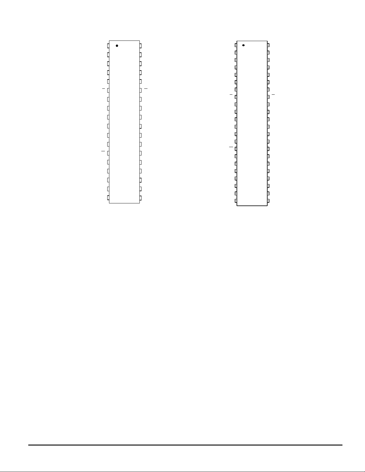
PIN ASSIGNMENTS
400 MIL SOJ TSOP TYPE II
NC
1
A
2
A
3
A
4
5
A
6
E
DQ
7
DQ
8
V
9
CC
V
10
SS
DQ
11
DQ
12
13
W
14
A
15
A
A
16
A
17
A
18
36
35
34
33A
32
31
30
29
28
27
26
25
24
23
22
21
20
19
NC
A
A
A
A
G
DQ
DQ
V
V
DQ
DQ
A
A
A
A
A
NC
SS
CC
1
NC
2
A
3
A
4
A
5
6
A
7
A
E
8
9
DQ
10
DQ
V
11
DD
12
V
SS
13
DQ
14
DQ
15
W
16
A
17
18
A
19
A
20
A
21
NC
22
NC
44
43
42
41
40
39
38
37
36
35
34
33
32
31
30
29
28
27
26
25
24
23
NC
NC
NC
A
A
A
A
G
DQ
DQ
V
V
DQ
DQ
A
A
AA
A
A
NC
NC
NC
SS
DD
MOTOROLA FAST SRAM
MCM6946
3
Page 4
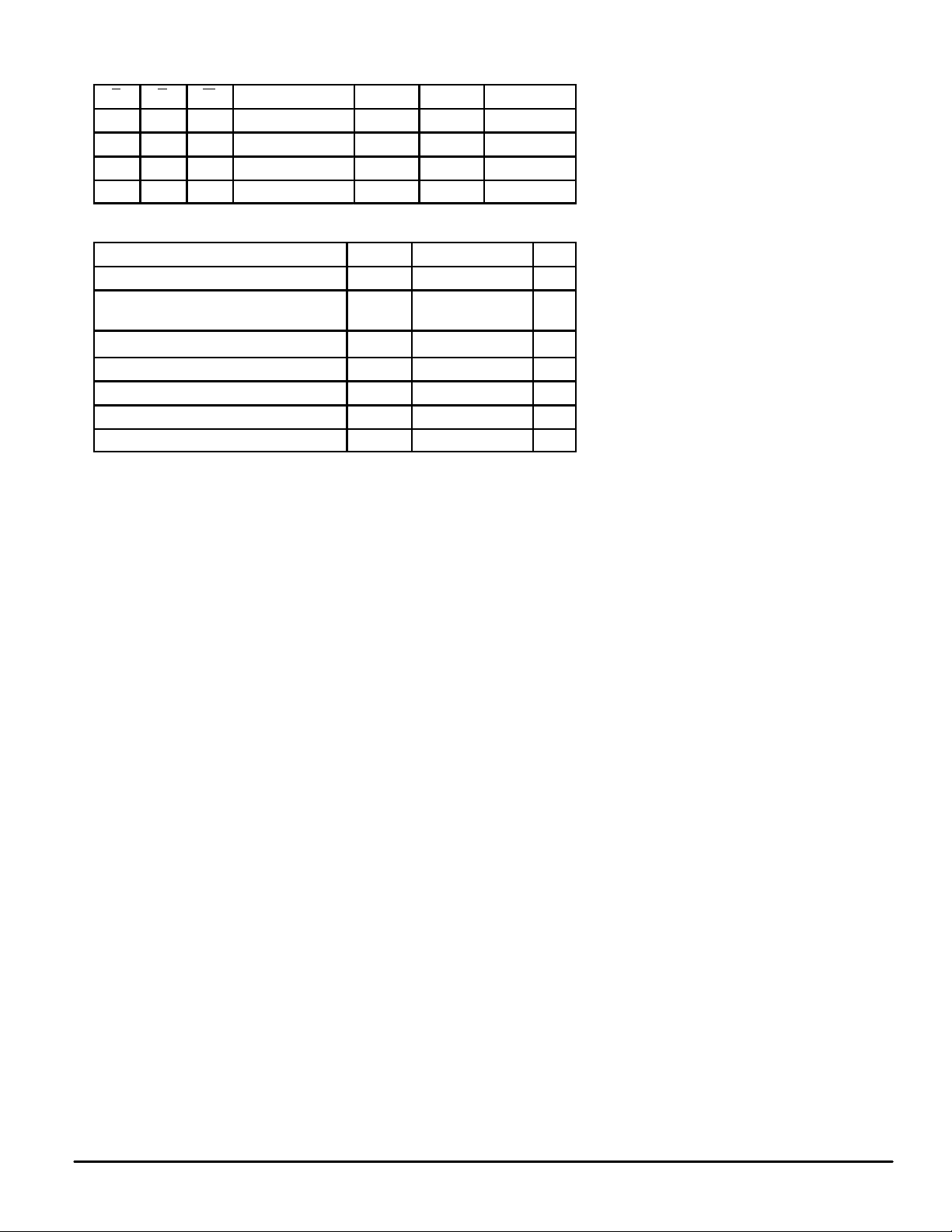
TRUTH TABLE (X = Don’t Care)
E G W Mode I/O Pin Cycle Current
H X X Not Selected High–Z — I
L H H Output Disabled High–Z — I
L L H Read D
L X L Write High–Z Write I
out
Read I
SB1
, I
CCA
CCA
CCA
SB2
ABSOLUTE MAXIMUM RATINGS (See Note)
Rating Symbol Value Unit
Power Supply Voltage Relative to V
Voltage Relative to VSS for Any Pin
Except V
Output Current (per I/O) I
Power Dissipation P
Temperature Under Bias T
Operating Temperature T
Storage Temperature — Plastic T
NOTE: Permanent device damage may occur if ABSOLUTE MAXIMUM RATINGS are
CC
exceeded. Functional operation should be restricted to RECOMMENDED OPERATING CONDITIONS. Exposure to higher than recommended voltages for
extended periods of time could affect device reliability.
SS
V
CC
Vin, V
out
bias
stg
– 0.5 to + 5.0 V
– 0.5 to VCC + 0.5 V
out
± 20
D
– 10 to + 85 °C
A
0 to + 70 °C
– 55 to + 150 °C
mA
1.0 W
This device contains circuitry to protect the
inputs against damage due to high static voltages or electric fields; however, it is advised
that normal precautions be taken to avoid
application of any voltage higher than maximum rated voltages to these high–impedance
circuits.
This BiCMOS memory circuit has been
designed to meet the dc and ac specifications
shown in the tables, after thermal equilibrium
has been established. The circuit is in a test
socket or mounted on a printed circuit board and
transverse air flow of at least 500 linear feet per
minute is maintained.
MCM6946
4
MOTOROLA FAST SRAM
Page 5

DC OPERA TING CONDITIONS AND CHARACTERISTICS
(VCC = 3.3 V – 5%, + 10%, TA = 0 to + 70°C, Unless Otherwise Noted)
RECOMMENDED OPERATING CONDITIONS
Parameter Symbol Min Typ Max Unit
Supply Voltage (Operating Voltage Range) V
Input High Voltage V
Input Low Voltage V
*VIL (min) = – 0.5 V dc; VIL (min) = – 2.0 V ac (pulse width ≤ 2.0 ns).
**VIH (max) = VCC + 0.3 V dc; VIH (max) = VCC + 2.0 V ac (pulse width ≤ 2.0 ns).
DC CHARACTERISTICS
Parameter Symbol Min Max Unit
Input Leakage Current (All Inputs, Vin = 0 to VCC) I
Output Leakage Current (E = VIH, V
Output Low Voltage (IOL = + 8.0 mA) V
Output High Voltage (IOH = – 4.0 mA) V
= 0 to VCC) I
out
POWER SUPPLY CURRENTS
Parameter Symbol 0 to 70°C Unit
AC Active Supply Current MCM6946–8: t
(I
= 0 mA, VCC = Max) MCM6946–10: t
out
AC Standby Current (VCC = Max, E = VIH, MCM6946–8: t
No Other Restrictions on Other Inputs) MCM6946–10: t
CMOS Standby Current (E ≥ VCC – 0.2 V, Vin ≤ VSS + 0.2 V or ≥ VCC – 0.2 V)
(VCC = Max, f = 0 MHz)
CC
IH
IL
MCM6946–12: t
MCM6946–15: t
MCM6946–12: t
MCM6946–15: t
AVAV
AVAV
AVAV
AVAV
AVAV
AVAV
AVAV
AVAV
3.135 3.3 3.6 V
2.2 — VCC + 0.3** V
– 0.5*
lkg(I)
lkg(O)
OL
OH
= 8 ns
= 10 ns
= 12 ns
= 15 ns
= 8 ns
= 10 ns
= 12 ns
= 15 ns
— 0.8 V
— ± 1.0 µA
— ± 1.0 µA
— 0.4 V
2.4 — V
I
CC
I
SB1
I
SB2
195
185
180
175
55
50
50
45
20
mA
mA
mA
CAPACITANCE (f = 1.0 MHz, dV = 3.3 V, T
Parameter Symbol Typ Max Unit
Input Capacitance All Inputs Except Clocks and DQs
Input/Output Capacitance DQ C
= 25°C, Periodically Sampled Rather Than 100% Tested)
A
E
, G, W
C
in
C
ck
I/O
4
5
5 8 pF
6
8
pF
MOTOROLA FAST SRAM
MCM6946
5
Page 6

AC OPERA TING CONDITIONS AND CHARACTERISTICS
(VCC = 3.3 V – 5%, + 10%, TA = 0 to + 70°C, Unless Otherwise Noted)
Input Pulse Levels 0 to 3.0 V. . . . . . . . . . . . . . . . . . . . . . . . . . . . . . . . .
Input Rise/Fall Time 2 ns. . . . . . . . . . . . . . . . . . . . . . . . . . . . . . . . . . . .
Input Timing Measurement Reference Level 1.5 V. . . . . . . . . . . . . . .
Output Timing Measurement Reference Level 1.5 V. . . . . . . . . . . . .
Output Load See Figure 1. . . . . . . . . . . . . . . . . . . . . . . . . . . . . . . . . . . .
READ CYCLE TIMING (See Notes 1 and 2)
MCM6946–8 MCM6946–10 MCM6946–12 MCM6946–15
Parameter Symbol
Read Cycle Time t
Address Access Time t
Enable Access Time t
Output Enable Access Time t
Output Hold from Address Change t
Enable Low to Output Active t
Output Enable Low to Output Active t
Enable High to Output High–Z t
Output Enable High to Output High–Z t
NOTES:
1. W
is high for read cycle.
2. Product sensitivities to noise require proper grounding and decoupling of power supplies as well as minimization or elimination of bus
contention conditions during read and write cycles.
3. All read cycle timings are referenced from the last valid address to the first transitioning address.
4. Addresses valid prior to or coincident with E
5. At any given voltage and temperature, t
to device.
6. Transition is measured ± 200 mV from steady–state voltage.
7. This parameter is sampled and not 100% tested.
8. Device is continuously selected (E
AVAV
AVQV
ELQV
GLQV
AXQX
ELQX
GLQX
EHQZ
GHQZ
EHQZ
≤ VIL, G ≤ VIL).
Min Max Min Max Min Max Min Max
8 — 10 — 12 — 15 — ns 3
— 8 — 10 — 12 — 15 ns
— 8 — 10 — 12 — 15 ns 4
— 4 — 5 — 6 — 7 ns
2 — 2 — 2 — 2 — ns
3 — 3 — 3 — 3 — ns 5, 6, 7
0 — 0 — 0 — 0 — ns 5, 6, 7
0 4 0 5 0 6 0 7 ns 5, 6, 7
0 4 0 5 0 6 0 7 ns 5, 6, 7
going low.
max t t
ELQX
min, and t
GHQZ
max t t
min, both for a given device and from device
GLQX
Unit Notes
OUTPUT
Z0 = 50
Ω
RL = 50
VL = 1.5 V
Ω
Figure 1. AC Test Load
TIMING LIMITS
The table of timing values shows either a minimum
or a maximum limit for each parameter. Input requirements are specified from the external system point of
view. Thus, address setup time is shown as a minimum since the system must supply at least that much
time. On the other hand, responses from the memory
are specified from the device point of view. Thus, the
access time is shown as a maximum since the device
never provides data later than that time.
MCM6946
6
MOTOROLA FAST SRAM
Page 7

A (ADDRESS)
READ CYCLE 1 (See Note 8)
t
AVAV
t
AXQX
Q (DATA OUT)
A (ADDRESS)
E (CHIP ENABLE)
(OUTPUT ENABLE)
G
Q (DATA OUT)
SUPPLY CURRENT
I
CC
I
SB
HIGH–Z
t
AVQV
READ CYCLE 2 (See Note 4)
t
AVAV
t
ELQV
t
ELQX
t
t
GLQX
t
AVQV
GLQV
DATA VALID
DATA VALIDPREVIOUS DATA VALID
t
EHQZ
t
GHQZ
MOTOROLA FAST SRAM
MCM6946
7
Page 8

WRITE CYCLE 1 (W Controlled; See Notes 1, 2, and 3)
MCM6946–8 MCM6946–10 MCM6946–12 MCM6946–15
Parameter Symbol
Write Cycle Time t
Address Setup Time t
Address Valid to End of W rite t
Address Valid to End of Write (G High) t
Write Pulse Width t
Write Pulse Width (G High) t
Data Valid to End of W rite t
Data Hold Time t
Write Low to Data High–Z t
Write High to Output Active t
Write Recovery Time t
NOTES:
1. A write occurs during the overlap of E
2. Product sensitivities to noise require proper grounding and decoupling of power supplies as well as minimization or elimination of bus
contention conditions during read and write cycles.
3. If G
goes low coincident with or after W goes low, the output will remain in a high–impedance state.
4. All write cycle timings are referenced from the last valid address to the first transitioning address.
5. Transition is measured ± 200 mV from steady–state voltage.
6. This parameter is sampled and not 100% tested.
7. At any given voltage and temperature, t
AVAV
AVWL
AVWH
AVWH
WLWH
t
WLEH
WLWH
t
WLEH
DVWH
WHDX
WLQZ
WHQX
WHAX
low and W low.
WLQZ
Min Max Min Max Min Max Min Max
8 — 10 — 12 — 15 — ns 4
0 — 0 — 0 — 0 — ns
8 — 9 — 10 — 12 — ns
7 — 8 — 9 — 10 — ns
8 — 9 — 10 — 12 — ns
7 — 8 — 9 — 10 — ns
5 — 5 — 6 — 7 — ns
0 — 0 — 0 — 0 — ns
0 4 0 5 0 6 0 7 ns 5, 6, 7
3 — 3 — 3 — 3 — ns 5, 6, 7
0 — 0 — 0 — 0 — ns
max < t
min, both for a given device and from device to device.
WHQX
Unit Notes
A (ADDRESS)
E (CHIP ENABLE)
W (WRITE ENABLE)
D (DATA IN)
Q (DATA OUT)
WRITE CYCLE 1 (W Controlled; See Notes 1, 2, and 3)
t
AVAV
t
AVWH
t
WLWH
t
WLEH
t
AVWL
t
WLQZ
HIGH–Z
t
DVWH
DATA VALID
HIGH–Z
t
WHAX
t
WHDX
t
WHQX
MCM6946
8
MOTOROLA FAST SRAM
Page 9

WRITE CYCLE 2 (E Controlled; See Notes 1, 2, and 3)
MCM6946–8 MCM6946–10 MCM6946–12 MCM6946–15
Parameter Symbol
Write Cycle Time t
Address Setup Time t
Address Valid to End of W rite t
Address Valid to End of Write (G High) t
Enable Pulse Width t
Enable Pulse Width (G High) t
Data Valid to End of W rite t
Data Hold Time t
Write Recovery Time t
NOTES:
1. A write occurs during the overlap of E
2. Product sensitivities to noise require proper grounding and decoupling of power supplies as well as minimization or elimination of bus
contention conditions during read and write cycles.
3. If G
goes low coincident with or after W goes low, the output will remain in a high–impedance state.
4. All write cycle timing is referenced from the last valid address to the first transitioning address.
5. If E
goes low coincident with or after W goes low, the output will remain in a high–impedance condition.
6. If E
goes high coincident with or before W goes high, the output will remain in a high–impedance condition.
AVAV
AVEL
AVEH
AVEH
ELEH,
t
ELWH
ELEH,
t
ELWH
DVEH
EHDX
EHAX
low and W low.
Min Max Min Max Min Max Min Max
8 — 10 — 12 — 15 — ns 4
0 — 0 — 0 — 0 — ns
7 — 9 — 10 — 12 — ns
7 — 8 — 9 — 10 — ns
8 — 9 — 10 — 12 — ns 5, 6
7 — 8 — 9 — 10 — ns 5, 6
5 — 5 — 6 — 7 — ns
0 — 0 — 0 — 0 — ns
0 — 0 — 0 — 0 — ns
Unit Notes
A (ADDRESS)
(CHIP ENABLE)
E
W
(WRITE ENABLE)
D (DATA IN)
Q (DATA OUT)
Motorola Memory Prefix
WRITE CYCLE 2 (E Controlled; See Notes 1, 2, and 3)
t
AVAV
t
t
AVEL
AVEH
HIGH–Z
t
ELEH
t
ELWH
t
DVEH
DATA VALID
ORDERING INFORMATION
(Order by Full Part Number)
MCM 6946 XX XX XX
Shipping Method (R = Tape and Reel, Blank = Rails)
t
EHAX
t
EHDX
Part Number
Full Part Numbers — MCM6946YJ8 MCM6946YJ10 MCM6946YJ12 MCM6946YJ15
MOTOROLA FAST SRAM
Speed (8 = 8 ns, 10 = 10 ns, 12 = 12 ns,
15 = 15 ns)
Package (YJ = 400 mil SOJ, TS = 44–Lead
TSOP Type II)
MCM6946YJ8R MCM6946YJ10R MCM6946YJ12R MCM6946YJ15R
MCM6946TS8 MCM6946TS10 MCM6946TS12 MCM6946TS15
MCM6946TS8R MCM6946TS10R MCM6946TS12R MCM6946TS15R
MCM6946
9
Page 10

P ACKAGE DIMENSIONS
YJ PACKAGE
400 MIL SOJ
CASE 893–02
Y0.015 (0.381) T
2 ZONES 18 PLACES
NOTE 3
0.007 (0.17) X
36 19
118
A
M
–X–
S
Y
T
S
C
E
–Y–
BP
R
R/2
36X R
R1
N36X
NOTES:
1. DIMENSIONING AND TOLERANCING PER ANSI
Y14.5M, 1982.
2. CONTROLLING DIMENSION: INCH.
3. TO BE DETERMINED AT PLANE –T–.
4. DIMENSION A AND B DO NOT INCLUDE MOLD
PROTRUSION. MOLD PROTRUSION SHALL NOT
EXCEED 0.006 (0.15) PER SIDE.
5. DIMENSION A AND B INCLUDE MOLD MISMATCH
AND ARE DETERMINED AT THE PARTING LINE.
DIM MIN MAX MIN MAX
A 0.920 0.930 23.37 23.62
B 0.395 0.405 10.03 10.29
C 0.128 0.148 3.25 3.76
D 0.015 0.020 0.38 0.51
E 0.082 ––– 2.08 –––
F 0.026 0.032 0.66 0.81
G 0.050 BSC 1.27 BSC
K 0.035 0.55 0.90 1.40
F36X
L 0.025 BSC 0.64 BSC
N 0.035 0.045 0.90 1.14
P 0.435 0.445 1 1.05 11.30
R 0.370 BSC 9.40 BSC
R1 0.030 0.040 0.76 1.02
MILLIMETERSINCHES
VIEW A
2X
34X
K
L
G
0.004 (0.1) T
SEATING
–T–
PLANE
D36X
0.007 (0.17) X
M
NOTE 3
S
Y
T
S
VIEW A
MCM6946
10
MOTOROLA FAST SRAM
Page 11

TS PACKAGE
44–LEAD
TSOP TYPE II
CASE 924A–02
B
44 23
VIEW A
E1
AA
122
D
A
44X
0.004 (0.1) C
SEATING
PLANE
e4X
/2
e
42X
C
c
b
M
0.2 C
SECTION A–A
40 PLACES
B
A1
L
VIEW A
ROTATED 90 CLOCKWISE
_
q
A2
A
NOTES:
1. DIMENSIONINS AND TOLERANCING PER ASME
Y14.5M, 1994.
2. DIMENSIONS IN MILLIMETER.
3. DIMENSION D1 AND E1 DO NOT INCLUDE MOLD
PROTRUSION. ALLOWABLE MOLD PROTRUSION
IS 0.15 PER SIDE.
4. DIMENSION b DOES NOT INCLUDE DAMBAR
PROTRUSIONS. DAMBAR PROTRUSION SHALL
NOT CAUSE THE LEAD WIDTH TO EXCEED 0.58.
DIM MIN MAX
A ––– 1.20
A1 0.05 0.15
A2 0.95 1.05
b 0.30 0.45
c 0.12 0.21
D 18.28 18.54
e 0.80 BSC
E 11.56 11.96
E1 10.03 10.29
L 0.40 0.60
q
22X E
M
0.2 C
MILLIMETERS
0 5
__
B
Motorola reserves the right to make changes without further notice to any products herein. Motorola makes no warranty , representation or guarantee regarding
the suitability of its products for any particular purpose, nor does Motorola assume any liability arising out of the application or use of any product or circuit, and
specifically disclaims any and all liability, including without limitation consequential or incidental damages. “T ypical” parameters which may be provided in Motorola
data sheets and/or specifications can and do vary in different applications and actual performance may vary over time. All operating parameters, including “Typicals”
must be validated for each customer application by customer’s technical experts. Motorola does not convey any license under its patent rights nor the rights of
others. Motorola products are not designed, intended, or authorized for use as components in systems intended for surgical implant into the body, or other
applications intended to support or sustain life, or for any other application in which the failure of the Motorola product could create a situation where personal injury
or death may occur. Should Buyer purchase or use Motorola products for any such unintended or unauthorized application, Buyer shall indemnify and hold Motorola
and its officers, employees, subsidiaries, affiliates, and distributors harmless against all claims, costs, damages, and expenses, and reasonable attorney fees
arising out of, directly or indirectly, any claim of personal injury or death associated with such unintended or unauthorized use, even if such claim alleges that
Motorola was negligent regarding the design or manufacture of the part. Motorola and are registered trademarks of Motorola, Inc. Motorola, Inc. is an Equal
Opportunity/Affirmative Action Employer.
How to reach us:
USA/EUROPE/Locations Not Listed: Motorola Literature Distribution; JAPAN: Nippon Motorola Ltd.: SPD, Strategic Planning Office, 141,
P.O. Box 5405, Denver , Colorado, 80217. 1-303-675-2140 or 1-800-441-2447 4-32-1 Nishi-Gotanda, Shagawa-ku, Tokyo, Japan. 03-5487-8488
Mfax: RMFAX0@email.sps.mot.com – TOUCHTONE 1-602-244-6609 ASIA/PACIFIC: Motorola Semiconductors H.K. Ltd.; 8B Tai Ping Industrial Park,
Motorola Fax Back System – US & Canada ONLY 1-800-774-1848 51 Ting Kok Road, Tai Po, N.T., Hong Kong. 852-26629298
HOME PAGE: http://motorola.com/sps/ CUSTOMER FOCUS CENTER: 1-800-521-6274
MOTOROLA FAST SRAM
– http://sps.motorola.com/mfax/
◊
Mfax is a trademark of Motorola, Inc.
MCM6946/D
MCM6946
11
 Loading...