

Datasheet MCM69D536TQ6R, MCM69D536TQ8, MCM69D536TQ8R, MCM67J618AFN5, MCM69D536TQ6 Datasheet (Motorola)
...Page 1
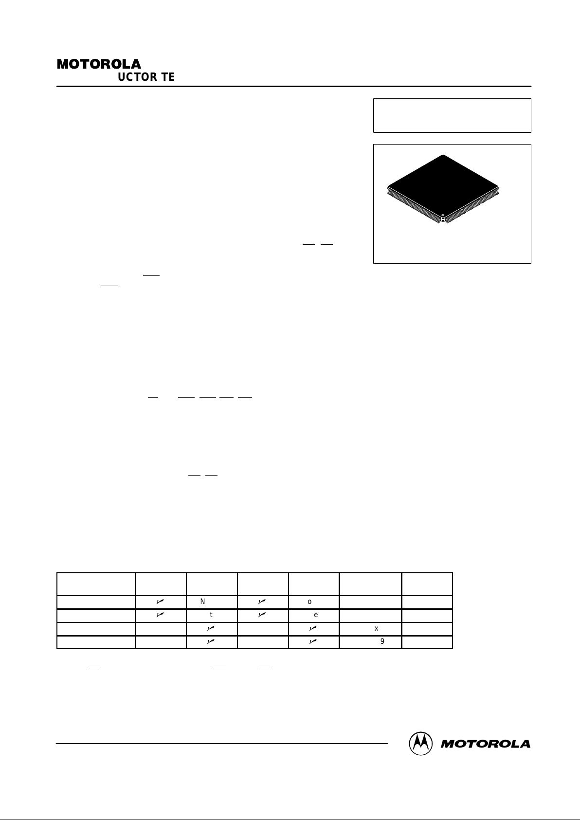
MCM69D536
1
MOTOROLA FAST SRAM
32K x 36 Bit Synchronous
Dual I/O, Dual Address SRAM
The MCM69D536 is a 1M–bit static random access memory, organized as 32K
words of 36 bits. It features common data input and data output buffers and
incorporates input and output registers on–board with high speed SRAM.
The MCM69D536 allows the user to concurrently perform reads, writes, or
pass–through cycles in combination on the two data ports. The two address ports
(AX, AY) determine the read or write locations for their respective data ports
(DQX, DQY).
The synchronous design allows for precise cycle control with the use of an
external single clock (K). All signal pins except output enables (GX
, GY) are
registered on the rising edge of clock (K).
The pass–through feature allows data to be passed from one port to the other,
in either direction. The PTX
input must be asserted to pass data from port X to
port Y. The PTY
will likewise pass data from port Y to port X. A pass–through
operation takes precedence over a read operation.
For the case when AX and AY are the same, certain protocols are followed. If
both ports are read, the reads occur normally . If one port is written and the other
is read, the read from the array will occur before the data is written. If both ports
are written, only the data on DQY will be written to the array.
• Single 3.3 V ± 5% Power Supply
• Fast Access Times: 6/8 ns Max
• Throughput of 2.98 Gigabits/Second
• Single Clock Operation
• Address, Data Input, E1
, E2, PTX, PTY, WX, WY, and Data Output
Registers On–Chip
• 83 MHz Maximum Clock Frequency
• Self–Timed Write
• Two Bi–Directional Data Buses
• Can be Configured as Separate I/O
• Pass–Through Feature
• Asynchronous Output Enables (GX
, GY)
• L VTTL Compatible I/O
• Concurrent Reads and Writes
• 176–Pin TQFP Package
Suggested Applications
— ATM — Ethernet Switches — Routers
— Cell/Frame Buffers — SNA Switches — Shared Memory
Product Family Configurations
Part
Number
Dual
Address
Single
Address
Dual
I/O
Separate
I/O
Configuration V
DD
MCM69D536
n
Note 1
n
Note 2 32K x 36 3.3 V
MCM69D618
n
Note 1
n
Note 2 64K x 18 3.3 V
MCM67Q709A
n n
128K x 9 5.0 V
MCM67Q909
n n
512K x 9 5.0 V
NOTES:
1. Tie AX and AY address ports together for the part to function as a single address part.
2. Tie GX
high for DQX to be inputs and tie WY high and GY low for DQY to be outputs.
Order this document
by MCM69D536/D
MOTOROLA
SEMICONDUCTOR TECHNICAL DATA
MCM69D536
TQ PACKAGE
176 LEAD TQFP
CASE 1101–01
REV 4
1/16/98
Motorola, Inc. 1998
Page 2
MCM69D536
2
MOTOROLA FAST SRAM
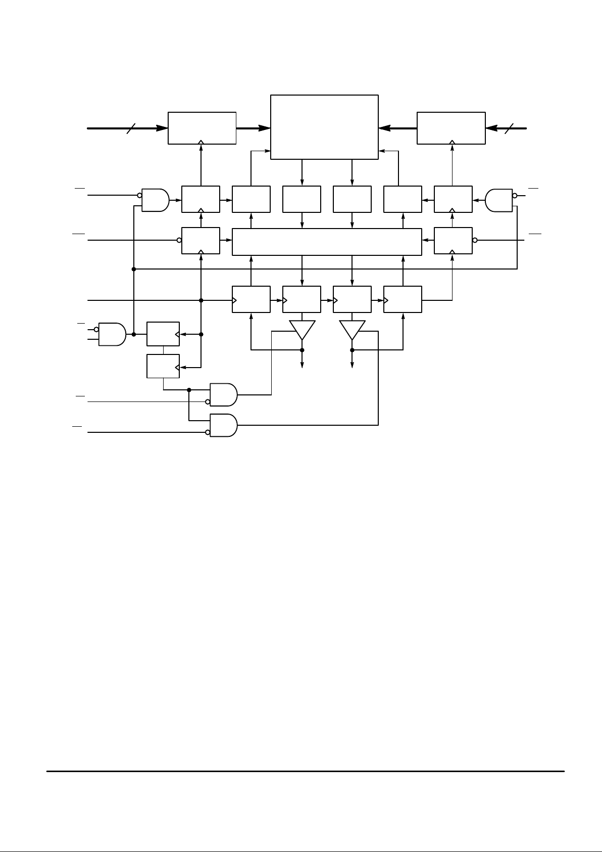
AX
E1
WX
BLOCK DIAGRAM
PTX
ADDRESS
REGISTER
32K x 36 ARRAY
GX
E2
ADDRESS
REGISTER
15
WRITE X
REGISTER
PTX
REGISTER
PASS–THROUGH
DQX
AY
WRITE
DRIVER
SENSE
AMPS
SENSE
AMPS
WRITE
DRIVER
WRITE Y
REGISTER
WY
PTY
REGISTER
PTY
DATA IN
REGISTER
OUTPUT
REGISTER
OUTPUT
REGISTER
DATA IN
REGISTER
ENABLE
REG 1
GY
DQY
15
ENABLE
REG 2
K
K
Page 3
MCM69D536
3
MOTOROLA FAST SRAM
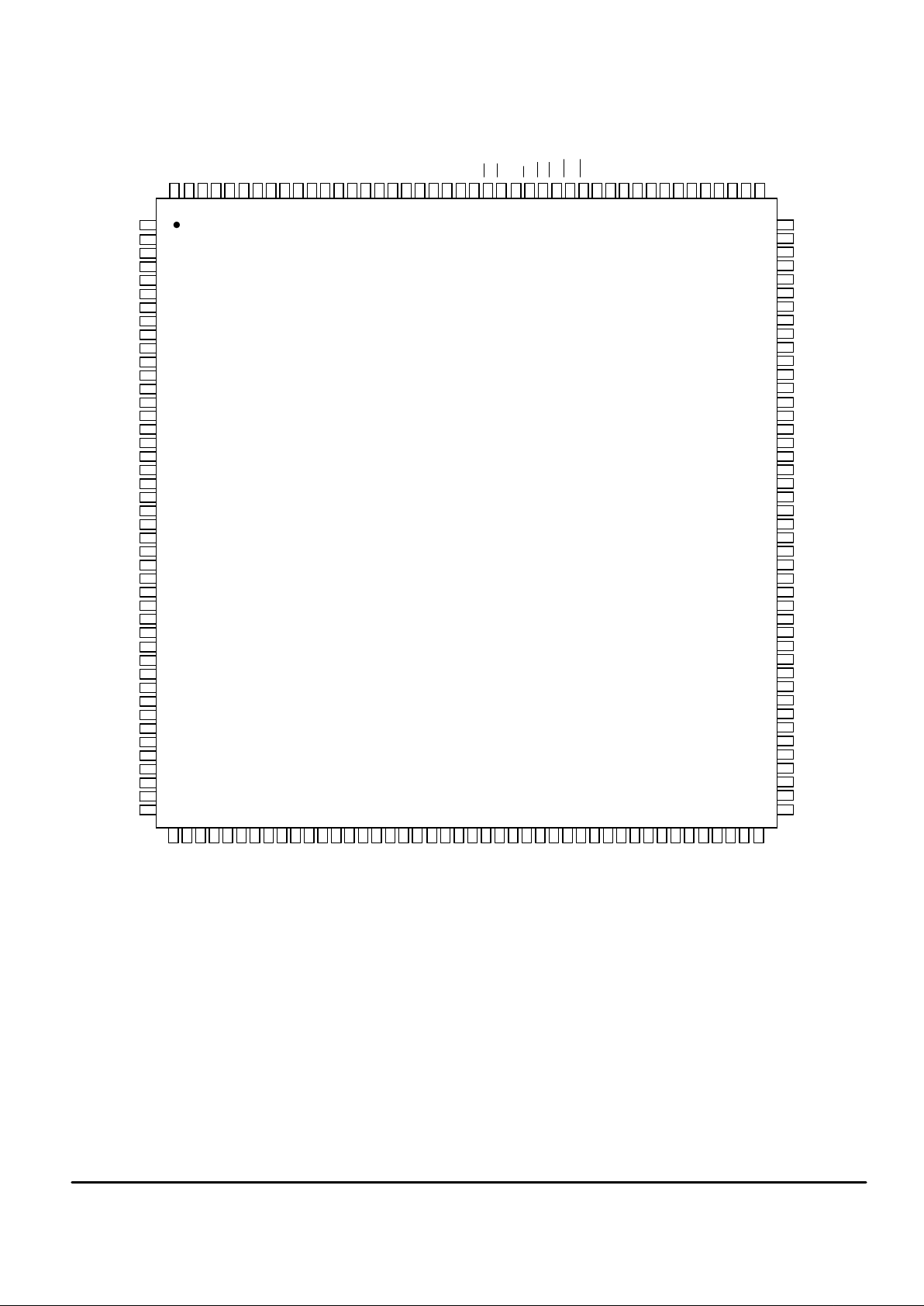
PIN ASSIGNMENT
DQX20
51 524849 50 56 575354 55 59605845 46 47 64636261
V
DD
V
SS
V
DD
V
SS
DQY20
DQX21
DQY21
DQX22
DQY22
DQX23
DQY23
DQX24
DQX35
DQY34
DQX34
V
SSi
DQY35
DQX25
DQY24
V
SS
DQY28
DQX28
DQY25
V
DD
V
SS
DQY27
DQX27
V
SSi
10
9
12
11
15
14
13
17
16
20
19
18
21
22
23
24
25
26
27
28
29
30
7
6
5
4
3
2
1
8
V
DD
DQX26
DQY26
V
DD
V
SS
DQY29
71 726968 70 76 7773 74 75 79 8078656667 84838281
DQY0
NCNCNC
DQX0
NC
88878685
DQY1
DQX1
DQY30
V
DD
V
SS
V
DD
V
SS
DQX30
DQY31
DQX31
DQY32
DQX32
DQY33
DQX33
V
SSi
DQX29
40
39
42
41
44
43
37
36
35
34
33
32
31
38
DQX2
V
DD
V
SS
V
DD
V
SS
DQY2
DQX3
DQY3
DQX4
DQY4
DQX5
DQY5
DQX6
DQX17
DQY16
DQX16
NC
NC
DQY17
DQX7
DQY6
V
SS
DQY10
DQX10
DQY7
V
DD
V
SS
DQY9
DQX9
V
SSi
98
97
100
99
103
102
101
105
104
108
107
106
109
110
111
112
113
114
115
116
117
118
95
94
93
92
91
89
90
96
V
DD
DQX8
DQY8
V
DD
V
SS
DQY11
E2
GX
PTY
WX
WY
E1
PTX
NCKNC
NC
NC
NC
GY
NC
DQY18
AX7
AY6
AX6
DQX18
AY7
DQY19
DQX19
DQY12
V
DD
V
SS
V
DD
V
SS
DQX12
DQY13
DQX13
DQY14
DQX14
DQY15
DQX15
V
SSi
DQX11
128
127
130
129
132
131
125
124
123
122
121
120
119
126
170
175
174
173
172
168
169
165
164
167
176
171
166
158
157
162
161
160
159
163
150
155
154
153
152
148
149
145
144
147
156
151
138
137
142
141
140
139
143
134
133
136
135
146
V
SSi
V
SS
V
DD
V
SSi
AY5
AX5
AY4
AX4
AY3
AX3
AY2
AX2
AY1
AX1
AY0
AX0
V
SS
V
DD
AX10
AY10
AX11
AY11
AX12
AY12
AX13
AY13
AX14
AY14
V
DD
V
SS
V
SSi
V
SSi
V
DD
V
SS
AX9
AY9
AX8
AY8
VDDV
SS
NC
NC
V
SSi
V
SS
V
SSi
V
DD
Page 4
MCM69D536
4
MOTOROLA FAST SRAM
PIN DESCRIPTIONS
Pin Locations Symbol Type Description
65, 63, 61, 59, 57, 55, 169, 167,
145, 143, 68, 70, 72, 74, 76
AX0 –
AX14
Input Address Port X. Never allow floating addresses for inputs AX0 – AX14.
A pullup resistor is needed.
64, 62, 60, 58, 56, 54, 168, 166,
144, 142, 69, 71, 73, 75, 77
AY0 –
AY14
Input Address Port Y. Never allow floating addresses for inputs AY0 – A Y14.
A pullup resistor is needed.
82, 86, 90, 94, 96, 100, 102, 106, 108,
113. 115, 119, 121, 125, 127, 131,
135, 139, 170, 174, 2, 6, 8, 12, 14, 18,
20, 25, 27, 31, 33, 37, 39, 43, 47, 51
DQX0 –
DQX35
I/O Data Input/Output Port X.
83, 87, 91, 95, 97, 101, 103, 107, 109,
112, 114, 118, 120, 124, 126, 130, 134,
138, 171, 175, 3, 7, 9, 13, 15, 19, 21,
24, 26, 30, 32, 36, 38, 42, 46, 50
DQY0 –
DQY35
I/O Data Input/Output Port Y.
150 E1 Input Synchronous Chip Enable: Active low.
151 E2 Input Synchronous Chip Enable: Active high.
152 GX Input Asynchronous Output Enable Port X Input:
Low — enables output buffers (DQXx pins).
High — DQXx pins are high impedance.
153 GY Input Asynchronous Output Enable Port Y Input:
Low — enables output buffers (DQYx pins).
High — DQYx pins are high impedance.
156 K Input Clock: This signal registers the address, data in, and all control signals
except G
.
146 PTX Input Pass–Through Port X.
147 PTY Input Pass–Through Port Y.
148 WX Input Synchronous Write Enable Port X.
149 WY Input Synchronous Write Enable Port Y.
4, 10, 16, 22, 28, 34, 40, 49,
67, 84, 92, 98, 104, 110,
116, 122, 128, 137, 155, 172
V
DD
Supply + 3.3 V Power Supply.
5, 11, 17, 23, 29, 35, 41, 48,
66, 85, 93, 99, 105, 111,
117, 123. 129, 136, 154, 173
V
SS
Supply Ground.
1, 44, 45, 52, 53, 88,
89, 132, 133, 165, 176
V
SSi
Input Bonded to die flag. No chip current flows through these pins.
78– 81, 140, 141, 157 – 164 NC — No Connection: There is no connection to the chip.
Page 5
MCM69D536
5
MOTOROLA FAST SRAM
TRUTH TABLE (See Notes 1 through 5)
Input at tn Clock
Operation Number
E1 E2 WX WY PTX PTY Operation
1 H X X X X X Deselected
2 X L X X X X Deselected
3 L H 0 X X X Write X Port
4 L H X 0 X X Write Y Port
5 L H X X 0 X Pass–Through X to Y
6 L H X X X 0 Pass–Through Y to X
7 L H 1 X 1 1 Read X
8 L H X 1 1 1 Read Y
NOTES:
1. GX
/GY must be controlled to avoid bus contention issues during write and pass–through cycles.
2. Operation numbers 3 – 6 can be used in any combination.
3. Operation numbers 4 and 7, 3 and 8, 7 and 8 can be combined.
4. Operation number 5 can not be combined with operation number 7 or 8 because pass–through takes precedence over a read operation.
5. Operation number 6 can not be combined with operation number 7 or 8 because pass–through takes precedence over a read operation.
K
ADDRESS & CONTROL
VALID
t
n
tn +
1
VALID
DATA INPUT D
VALID
DATA OUTPUT Q
PIPELINED READ ACCESS
PASS–THROUGH
ABSOLUTE MAXIMUM RATINGS (See Note)
Rating
Symbol Value Unit
Power Supply Voltage V
DD
– 0.5 to + 4.6 V
Voltage Relative to VSS for Any Pin
Except V
DD
Vin, V
out
– 0.5 to VDD + 0.5 V
Output Current I
out
± 20 mA
Power Dissipation P
D
TBD W
Temperature Under Bias T
bias
– 10 to + 85 °C
Operating Temperature T
A
0 to + 70 °C
Storage Temperature — Plastic T
stg
– 55 to + 125 °C
NOTE: Permanent device damage may occur if ABSOLUTE MAXIMUM RATINGS are
exceeded. Functional operation should be restricted to RECOMMENDED OPERATING CONDITIONS. Exposure to higher than recommended voltages for
extended periods of time could affect device reliability.
This is a synchronous device. All synchronous inputs must meet specified setup and hold
times with stable logic levels for
ALL
rising
edges of clock (K) while the device is selected.
This device contains circuitry to protect the
inputs against damage due to high static voltages or electric fields; however, it is advised
that normal precautions be taken to avoid
application of any voltage higher than maximum rated voltages to these high–impedance
circuits.
Page 6

MCM69D536
6
MOTOROLA FAST SRAM
PACKAGE THERMAL CHARACTERISTICS (See Note 1)
Rating
Symbol TQFP Unit Notes
Junction to Ambient (@ 200 lfm) Single–Layer Board
Four–Layer Board
R
θJA
40
35
°C/W 2
Junction to Board (Bottom) R
θJB
23 °C/W 3
Junction to Case (Top) R
θJC
9 °C/W 4
NOTES:
1. Junction temperature is a function of on–chip power dissipation, package thermal resistance, mounting site (board) temperature, ambient
temperature, air flow, board population, and board thermal resistance.
2. Per SEMI G38–87.
3. Indicates the average thermal resistance between the die and the printed circuit board.
4. Indicates the average thermal resistance between the die and the case top surface via the cold plate method (MIL SPEC–883 Method 1012.1).
DC OPERA TING CONDITIONS AND CHARACTERISTICS
(VDD = 3.3 V ± 5%, TA = 0 to + 70°C, Unless Otherwise Noted)
RECOMMENDED OPERATING CONDITIONS AND SUPPLY CURRENTS
Parameter Symbol Min Max Unit
Supply Voltage (Operating Voltage Range) V
DD
3.135 3.465 V
Input High Voltage V
IH
2.0 VDD + 0.5** V
Input Low Voltage V
IL
– 0.5* 0.8 V
Input Leakage Current (All Inputs, Vin = 0 to VDD) I
lkg(I)
— ± 1.0 µA
Output Leakage Current (E = VIH, V
out
= 0 to VDD) I
lkg(O)
— ± 1.0 µA
AC Supply Current (I
out
= 0 mA) (VDD = max, f = f
max
) MCM69D536–6 ns
MCM69D536–8 ns
I
DDA
—
—
300
300
mA
CMOS Standby Supply Current (Deselected, Clock (K) MCM69D536–6 ns
Cycle Time ≥ t
KHKH
, All Inputs Toggling at CMOS Levels MCM69D536–8 ns
Vin ≤ VSS + 0.2 V or ≥ VDD – 0.2 V)
I
SB1
—
—
100
100
mA
Output Low Voltage (IOL = + 8.0 mA) V
OL
— 0.4 V
Output High Voltage (IOH = – 4.0 mA) V
OH
2.4 V
DD
V
*VIL ≥ – 1.5 V for t ≤ t
KHKH
/2.
**VIH ≤ VDD + 1.0 V for t ≤ t
KHKH
/2.
CAPACITANCE (f = 1.0 MHz, dV = 3.0 V, T
A
= 0 to 70°C, Periodically Sampled Rather Than 100% Tested)
Parameter Symbol Max Unit
Address and Data Input Capacitance C
in
6 pF
Control Pin Input Capacitance C
in
6 pF
Output Capacitance C
out
8 pF
Page 7

MCM69D536
7
MOTOROLA FAST SRAM
AC OPERA TING CONDITIONS AND CHARACTERISTICS
(VDD = 3.3 V ± 5%, TA = 0 to + 70°C, Unless Otherwise Noted)
Input Timing Measurement Reference Level 1.5 V. . . . . . . . . . . . . . .
Input Pulse Levels 0 to 3.0 V. . . . . . . . . . . . . . . . . . . . . . . . . . . . . . . . .
Input Rise/Fall Time 3 ns. . . . . . . . . . . . . . . . . . . . . . . . . . . . . . . . . . . .
Output Timing Reference Level 1.5 V. . . . . . . . . . . . . . . . . . . . . . . . . .
Output Load Figure 1 Unless Otherwise Noted. . . . . . . . . . . . . . . . . .
READ/WRITE CYCLE TIMING (See Notes 1, 2, and 3)
MCM69D536–6 MCM69D536–8
Parameter Symbol Min Max Min Max Unit Notes
Cycle Time t
KHKH
12 — 15 — ns 1
Clock Access Time t
KHQV
— 6 — 8 ns
Clock Low Pulse Width t
KLKH
4 — 6 — ns
Clock High Pulse Width t
KHKL
4 — 6 — ns
Clock High to Data Output Active t
KHQX1
0 — 0 — ns
Clock High to Data Output Invalid t
KHQX2
2 — 2 — ns
Clock High to Data Output High–Z t
KHQZ
— 5 — 5 ns 2
Output Enable Low to Data Output Valid t
GLQV
— 6 — 8 ns
Output Enable Low to Data Output Low–Z t
GLQX
0
—
0 — ns
Output Enable High to Data Output High–Z t
GHQZ
— 5 — 8 ns 2
Setup Times: AWR0 – AWR14
ARD0 – ARD14
W
PT
E1, E2
D0 – D35
t
AVKH
t
AVKH
t
WVKH
t
PTVKH
t
EVKH
t
DVKH
2.5 — 3 — ns 3
Hold Times: AWR0 – AWR14
ARD0 – ARD14
W
PT
E1, E2
D0 – D35
t
KHAX
t
KHAX
t
KHWX
t
KHPTX
t
KHEX
t
KHDX
0.5 — 1 — ns 3
3
3
3
3
3, 4
NOTES:
1. All read and write cycles are referenced from K.
2. This parameter is sampled and not 100% tested.
3. This is a synchronous device. All synchronous inputs must meet the specified setup and hold times with stable logic levels for
ALL
rising
edges of clock (K) while the device is selected.
4. t
KHDX
minimum for Port Y only extends to 4.0 ns only for the special case when the Y– and X–address are identical on the same rising
clock edge.
OUTPUT
Z0 = 50
Ω
RL = 50
Ω
VL = 1.5 V
Figure 1. AC Test Load
Page 8

MCM69D536
8
MOTOROLA FAST SRAM
1
K
AX
E
t
KHKH t
KLKH
t
KHKL
2 3 4 5 6 7 8 9
GX
DQX
t
GLQV
t
GHQZ
t
KHQV
t
KHQX1
Q(1) Q(2) Q(3) Q(5) Q(6)
12
AY
13 14 15 16 6 7 19 20
GY
DQY
t
KHQZ
Q(12) Q(13) Q(14) Q(16) Q(6) Q(7)
Q(7)
t
GLQX
t
EVKH
t
KHEX
t
KHQV
PORT X
PORT Y
NOTE: E Low = E1 Low and E2 High. E High = E1 High or E2 Low.
t
AVKH
t
KHAX
READ CYCLE TIMING FROM BOTH PORTS (WX, WY, PTX, PTY HIGH)
Page 9

MCM69D536
9
MOTOROLA FAST SRAM
K
AX
E
t
KHKH
t
KLKH
t
KHKL
GX
DQX
AY
GY
D(2) D(3) D(4)
D(5) D(6)
D(8) D(9)
t
KHWX
PORT X
WX
PORT Y
WY
DQY
D(14) D(15) D(19)D(18)
t
WVKH
t
KHDX
t
DVKH
NOTE: E Low = E1 Low and E2 High. E High = E1 High or E2 Low.
PORT Y TAKES PRECEDENCE
OVER PORT X WHEN AX = AY
AND WRITING BOTH PORTS.
WRITE CYCLE TIMING TO BOTH PORTS (PTX, PTY HIGH)
1 2 3 4 5 6 7 8 9
12 13 14
15
5 6 18 19 20
Page 10

MCM69D536
10
MOTOROLA FAST SRAM
t
KHPTX
K
AX
E
t
KHKH
t
KLKH
t
KHKL
GX
DQX
AY
GY
D(2) D(3) D(X) D(Y) D(6)
t
KHQV
PORT X
WX
PORT Y
WY
DQY
t
KHQX2
t
KHDX
t
DVKH
E Low = E1 Low and E2 High. E High = E1 High or E2 Low.
NOTE: The timing diagram is valid for the opposite case as well, i.e., writing to Port Y and passing through to Port X.
PTX
PTY
D(3) D(X)
D(Y)
D(17)
t
KHQZ
t
PTVKH
WRITE TO PORT X AND PASS–THROUGH TO PORT Y (SEE NOTE)
1 2 3 4 5 6 7 8 9
12 13 14
15
16 17 18 19 20
Page 11

MCM69D536
11
MOTOROLA FAST SRAM
GY
DQY
D(PQR) D(XYZ) Q(PQR) D(JKL) Q(JKL)
PORT Y TAKES PRECEDENCE
OVER PORT X WHEN AX = AY
AND WRITING BOTH PORTS.
1
K
AX
t
KHKH
t
KLKH
t
KHKL
2 1 2 3
GX
DQX
D(ABC) D(DEF)
PORT X
WX
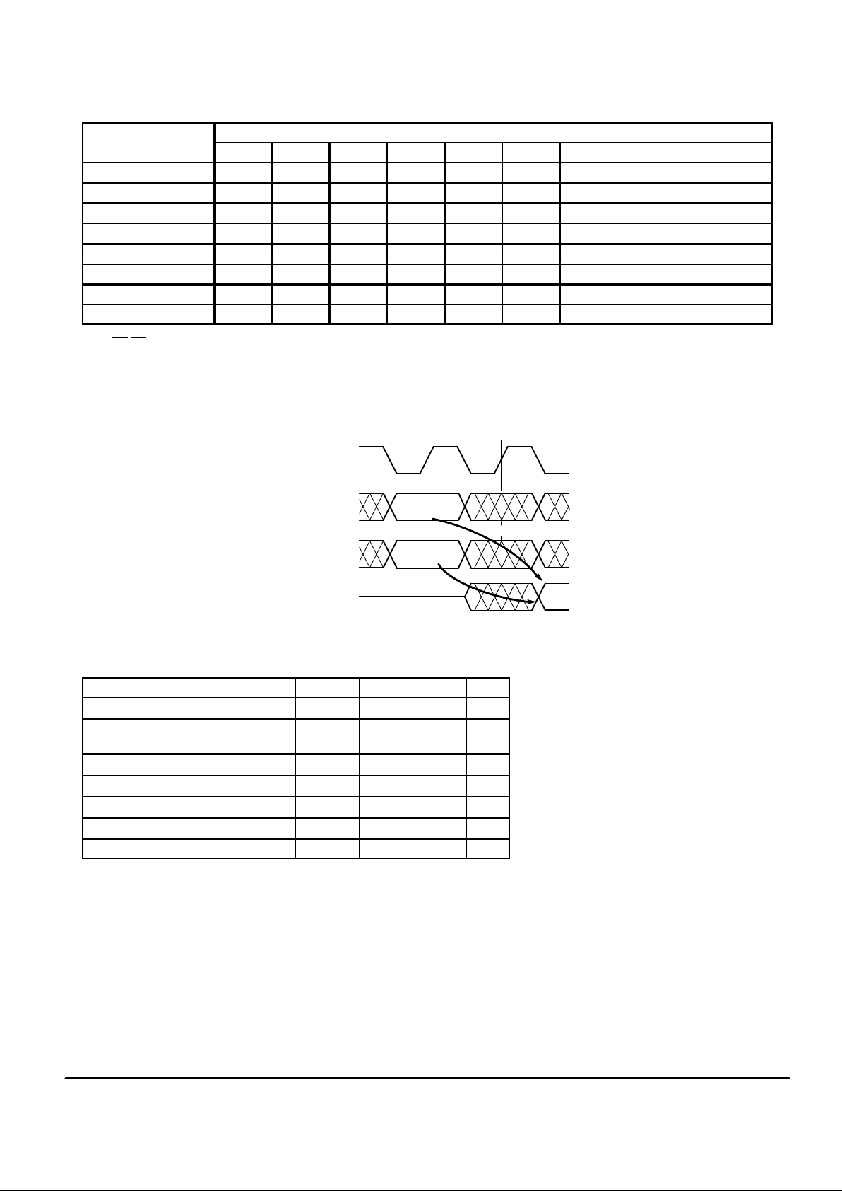
READ READ READ READ READ READ
Q(XYZ) Q(JKL)Q(PQR)
TRY TO
WRITE
TRY TO
WRITE
COMBINATION READ/WRITE WITH SAME ADDRESS ON EACH PORT
AY
WY
1 2 1 2 3
WRITE WRITE
READ READ READ WRITE READ READ
PORT Y
PTX = PTY = high.
D(Value) = Value is the input to the data port.
Q(Value) = Value is the output from the data port.
Page 12

MCM69D536
12
MOTOROLA FAST SRAM
Motorola Memory Prefix
Part Number
Package (TQ = TQFP)
Full Part Numbers — MCM69D536TQ6 MCM69D536TQ8
MCM69D536TQ6R MCM69D536TQ8R
Shipping Method (R = Tape and Reel,
Blank = Rails)
Speed (6 = 6ns, 8 = 8 ns)
MCM 69D536 XX XX X
ORDERING INFORMATION
(Order by Full Part Number)
Page 13

MCM69D536
13
MOTOROLA FAST SRAM
TQFP PACKAGE
176 LEAD
CASE 1101–01
P ACKAGE DIMENSIONS
_
C
L
–M–
B
NOTES:
1. DIMENSIONING AND TOLERANCING PER ANSI Y14.5M, 1982.
2. CONTROLLING DIMENSION: MILLIMETER.
3. DATUM PLANE –H– IS LOCATED AT BOTTOM OF LEAD AND IS
COINCIDENT WITH THE LEAD WHERE THE THE LEAD EXITS THE
PLASTIC BODY AT THE BOTTOM OF THE PARTING LINE.
4. DATUMS –L–, –M–, AND –N– TO BE DETERMINED AT DATUM PLANE
–H–.
5. DIMENSIONS S AND V TO BE DETERMINED AT SEATING PLANE –T–.
6. DIMENSIONS A AND B DO NOT INCLUDE MOLD PROTRUSION.
ALLOWABLE PROTRUSION IS 0.25 (0.010) PER SIDE. DIMENSIONS A
AND B DO INLCUDE MOLD MISMATCH AND ARE DETERMINED AT
DATUM PLANE –H–.
7. DIMENSION D DOES NOT INCLUDE DAMBAR PROTRUSION. DAMBAR
PROTRUSION SHALL NOT CAUSE THE LEAD WIDTH TO EXCEED 0.35
(0.014) MINIMUM SPACE BETWEEN PROTRUSION AND ADJACENT
LEAD 0.07 (0.003).
PIN 1
1
DIM MIN MAX
MILLIMETERS
A 24.00 BSC
A1 12.00 BSC
B 24.00 BSC
B1 12.00 BSC
C ––– 1.60
C1 0.05 –––
C2 1.35 1.45
D 0.17 0.23
E 0.45 0.75
F 0.17 0.27
G 0.50 BSC
J 0.09 0.20
K 0.50 REF
P 0.25 BSC
R1 0.10 0.20
S 26.00 BSC
S1 13.00 BSC
U 0.09 0.16
V 26.00 BSC
V1 13.00 BSC
W 0.20 REF
Z 1,00 REF
q
0 7
1 0 –––
2 12 REF
q
q
_
___
AB
AB
G
P
X=L, M, N
–X–
VIEW Y
C
L
ROTATED 90 CLOCKWISE
IDENT
SEATING
PLANE
GAGE
PLANE
q
A
A1
C2
W
1
Z
K
E
VIEW AA
q
0.25
R12X R
C1
S
0.05
M
0.08 T
BASE
PLATING
METAL
F
JU
VIEW Y
4X 44 TIPS
D
S
L–MSN
SECTION AB–AB
C
L
4X
3X
176 133
132
45 88
44 89
–N–
–L–
L–M NT0.20L–M NH0.20
S
S1
V1
B1
C
VIEW AA
V
–H–
–T–
2
q
4X
T0.08
Page 14

MCM69D536
14
MOTOROLA FAST SRAM
Motorola reserves the right to make changes without further notice to any products herein. Motorola makes no warranty , representation or guarantee regarding
the suitability of its products for any particular purpose, nor does Motorola assume any liability arising out of the application or use of any product or circuit, and
specifically disclaims any and all liability, including without limitation consequential or incidental damages. “T ypical” parameters which may be provided in Motorola
data sheets and/or specifications can and do vary in different applications and actual performance may vary over time. All operating parameters, including “Typicals”
must be validated for each customer application by customer’s technical experts. Motorola does not convey any license under its patent rights nor the rights of
others. Motorola products are not designed, intended, or authorized for use as components in systems intended for surgical implant into the body, or other
applications intended to support or sustain life, or for any other application in which the failure of the Motorola product could create a situation where personal injury
or death may occur. Should Buyer purchase or use Motorola products for any such unintended or unauthorized application, Buyer shall indemnify and hold Motorola
and its officers, employees, subsidiaries, affiliates, and distributors harmless against all claims, costs, damages, and expenses, and reasonable attorney fees
arising out of, directly or indirectly, any claim of personal injury or death associated with such unintended or unauthorized use, even if such claim alleges that
Motorola was negligent regarding the design or manufacture of the part. Motorola and are registered trademarks of Motorola, Inc. Motorola, Inc. is an Equal
Opportunity/Affirmative Action Employer.
Mfax is a trademark of Motorola, Inc.
How to reach us:
USA/EUROPE /Locations Not Listed: Motorola Literature Distribution; JAPAN: Nippon Motorola Ltd.: SPD, Strategic Planning Office, 141,
P.O. Box 5405, Denver, Colorado, 80217 . 1-303-675-2140 or 1-800-441-2447 4-32-1 Nishi-Gotanda, Shagawa-ku, Tokyo, Japan. 03-5487-8488
Mfax: RMFAX0@email.sps.mot.com – TOUCHTONE 1-602-244-6609 ASIA/PACIFIC: Motorola Semiconductors H.K. Ltd.; 8B Tai Ping Industrial Park,
Motorola Fax Back System – US & Canada ONLY 1-800-774-1848 51 Ting Kok Road, Tai Po, N.T., Hong Kong. 852-26629298
– http://sps.motorola.com/mfax/
HOME PAGE: http://motorola.com/sps/ CUSTOMER FOCUS CENTER: 1-800-521-6274
MCM69D536/D
◊
 Loading...