

Page 1
MCM67A618
1
MOTOROLA FAST SRAM
64K x 18 Bit Asynchronous/
Latched Address Fast Static RAM
The MCM67A618 is a 1,179,648 bit latched address static random access
memory organized as 65,536 words of 18 bits, fabricated with Motorola’s high–
performance silicon–gate BiCMOS technology . The device integrates a 64K x 18
SRAM core with advanced peripheral circuitry consisting of address and data input latches, active low chip enable, separate upper and lower byte write strobes,
and a fast output enable. This device has increased output drive capability supported by multiple power pins.
Address, data in, and chip enable latches are provided. When latch enables
(AL for address and chip enables and DL for data in) are high, the address, data
in, and chip enable latches are in the transparent state. If latch enables are tied
high the device can be used as an asynchronous SRAM. When latch enables are
low the address, data in, and chip enable latches are in the latched state. This
input latch simplifies read and write cycles by guaranteeing address and data–in
hold time in a simple fashion.
Dual write enables (LW
and UW) are provided to allow individually writeable
bytes. LW
controls DQ0 – DQ8 (the lower bits) while UW controls DQ9 – DQ17
(the upper bits).
Six pair of power and ground pins have been utilized and placed on the package for maximum performance.
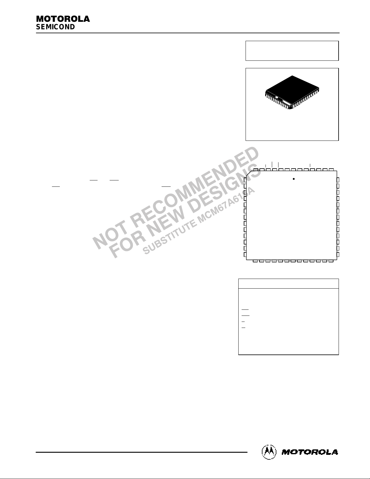
The MCM67A618 will be available in a 52–pin plastic leaded chip carrier
(PLCC).
This device is ideally suited for systems that require wide data bus widths,
cache memory, and tag RAMs.
• Single 5 V
± 5% Power Supply
• Fast Access Times: 10/12/15 ns Max
• Byte Writeable via Dual Write Enables
• Separate Data Input Latch for Simplified Write Cycles
• Address and Chip Enable Input Latches
• Common Data Inputs and Data Outputs
• Output Enable Controlled Three–State Outputs
• 3.3 V I/O Compatible
• High Board Density 52–Lead PLCC Package
PIN ASSIGNMENT
V
CC
DQ10
DQ9
V
SS
DQ11
DQ12
DQ13
DQ14
V
SS
V
CC
DQ15
DQ16
DQ17
DQ7
DQ6
V
CC
V
SS
DQ5
DQ4
DQ3
DQ2
V
SS
V
CC
DQ1
DQ0
8
9
10
11
12
13
14
15
16
17
18
19
20
46
45
44
43
42
41
40
39
38
37
36
35
34
4748495051521234567
33323130292827262524232221
SS
V
DQ8
CC
V
A4A3A2
A1
A5
A0
A15
A13
A14
A12
A11
V
SS
V
CC
AL
A8A9A10
G
A6A7E
UW
LW
DL
All power supply and ground pins must be connected for proper operation of the device.
PIN NAMES
A0 – A15 Address Inputs. . . . . . . . . . . . . . . .
AL Address Latch. . . . . . . . . . . . . . . . . . . . . .
DL Data Latch. . . . . . . . . . . . . . . . . . . . . . . . .
LW
Lower Byte Write Enable. . . . . . . . . . . .
UW
Higher Byte Write Enable. . . . . . . . . . . .
E
Chip Enable. . . . . . . . . . . . . . . . . . . . . . . . .
G
Output Enable. . . . . . . . . . . . . . . . . . . . . .
DQ0 – DQ17 Data Input/Output. . . . . . . . . . .
V
CC
+ 5 V Power Supply. . . . . . . . . . . . . . . .
V
SS
Ground. . . . . . . . . . . . . . . . . . . . . . . . . . .
Order this document
by MCM67A618/D
MOTOROLA
SEMICONDUCTOR TECHNICAL DATA
MCM67A618
FN PACKAGE
PLASTIC
CASE 778–02
REV 4
5/95
Motorola, Inc. 1994
Page 2
MCM67A618
2
MOTOROLA FAST SRAM
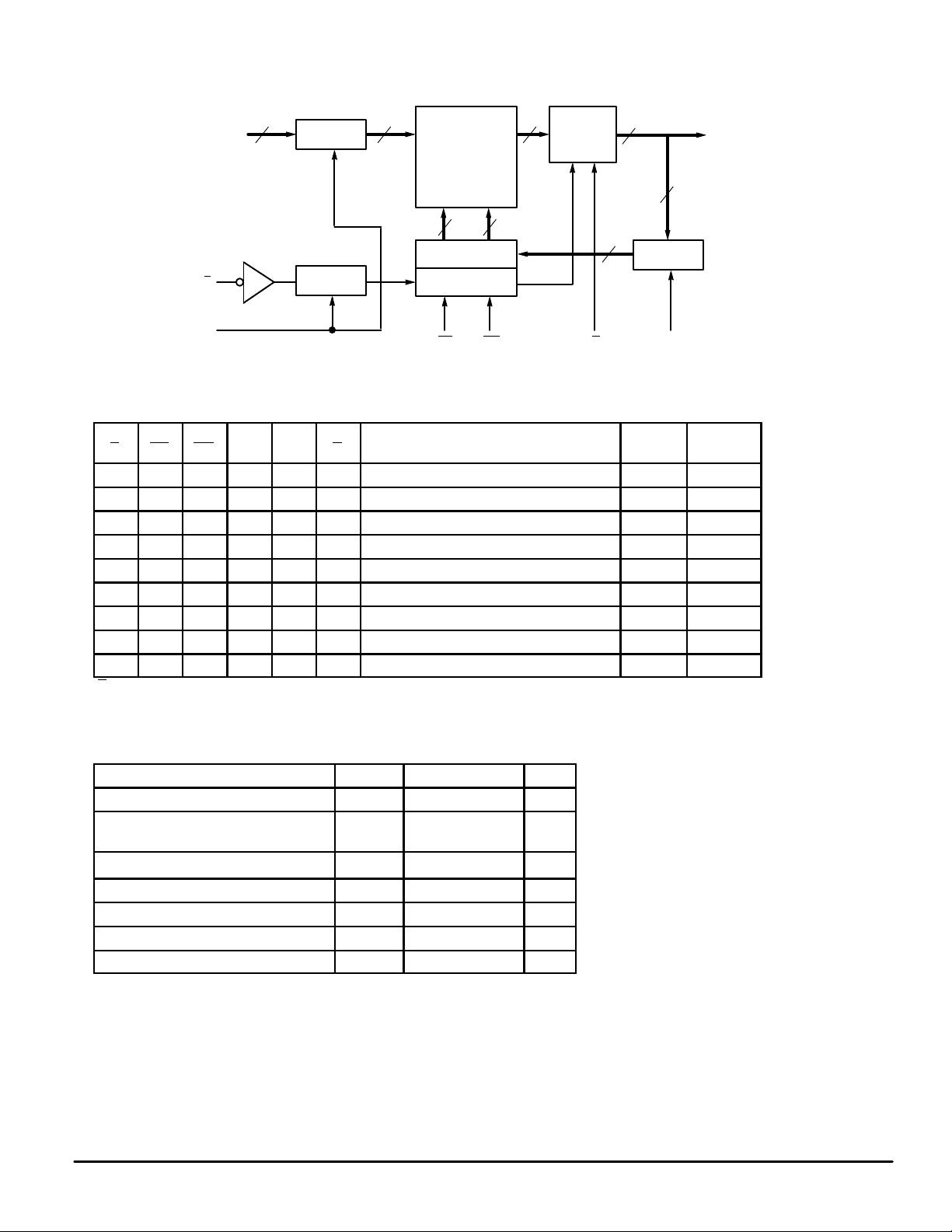
BLOCK DIAGRAM
A0 – A15
DQ0 – DQ17
MEMORY ARRAY
64K x 18
E
WRITE AMP
OUTPUT
BUFFER
CONTROL
16
18
AL
LW
UW G
16
18
18
LATCH
DL
18
9 9
LATCH
LATCH
TRUTH TABLE
E LW UW AL* DL* G Mode
Supply
Current
I/O
Status
H X X X X X Deselected Cycle I
SB
High–Z
L X X L X X Read or Write Using Latched Addresses I
CC
—
L X X H X X Read or Write Using Unlatched Addresses I
CC
—
L H H X X L Read Cycle I
CC
Data Out
L H H X X H Read Cycle I
CC
High–Z
L L L X L X Write Both Bytes Using Latched Data In I
CC
High–Z
L L L X H X Write Both Bytes Using Unlatched Data In I
CC
High–Z
L L H X X X Write Cycle, Lower Byte I
CC
High–Z
L H L X X X Write Cycle, Lower Byte I
CC
High–Z
*E and Addresses satisfy the specified setup and hold times for the falling edge of AL. Data–in satisfies the specified setup
*and hold times for falling edge of DL.
NOTE: This truth table shows the application of each function. Combinations of these functions are valid.
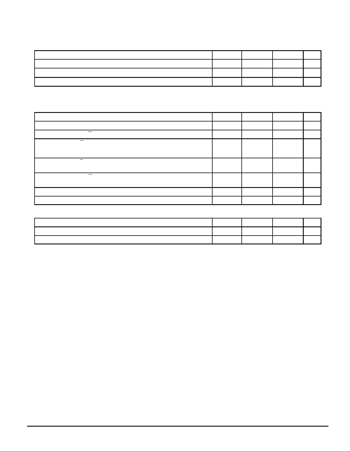
ABSOLUTE MAXIMUM RATINGS (Voltages Referenced to V
SS
= 0)
Rating
Symbol Value Unit
Power Supply Voltage V
CC
– 0.5 to 7.0 V
Voltage Relative to VSS for Any
Pin Except V
CC
Vin, V
out
– 0.5 to VCC + 0.5 V
Output Current (per I/O) I
out
± 30
mA
Power Dissipation P
D
1.6 W
Temperature Under Bias T
bias
– 10 to + 85 °C
Operating Temperature T
A
0 to + 70 °C
Storage Temperature T
stg
– 55 to + 125 °C
NOTE: Permanent device damage may occur if ABSOLUTE MAXIMUM RATINGS are
exceeded. Functional operation should be restricted to RECOMMENDED OPERATING CONDITIONS. Exposure to higher than recommended voltages for
extended periods of time could affect device reliability.
advised
that normal precautions be taken to avoid
application of any voltage higher than maximum rated voltages to this high–impedance
circuit.
This BiCMOS memory circuit has been
designed to meet the dc and ac specifications
shown in the tables, after thermal equilibrium
has been established.
This device contains circuitry that will ensure
the output devices are in High–Z at power up.
This device contains circuitry to protect the
inputs against damage due to high static
voltages or electric fields; however, it is
Page 3
MCM67A618
3
MOTOROLA FAST SRAM
DC OPERATING CONDITIONS AND CHARACTERISTICS
(VCC = 5.0 V ± 5%, TA = 0 to + 70°C, Unless Otherwise Noted)
RECOMMENDED OPERATING CONDITIONS
(Voltages referenced to VSS = 0 V)
Parameter
Symbol Min Max Unit
Supply Voltage (Operating Voltage Range) V
CC
4.75 5.25 V
Input High Voltage V
IH
2.2
VCC + 0.3**
V
Input Low Voltage V
IL
– 0.5*
0.8 V
** VIL (min) = – 0.5 V dc; VIL (min) = – 2.0 V ac (pulse width ≤ 20 ns) for I ≤ 20.0 mA.
** VIH (max) = VCC + 0.3 V dc; VIH (max) = VCC + 2.0 V ac (pulse width ≤ 20 ns) for I ≤ 20.0 mA.
DC CHARACTERISTICS
Parameter Symbol Min Max Unit
Input Leakage Current (All Inputs, Vin = 0 to VCC) I
lkg(I)
— ± 1.0 µA
Output Leakage Current (G = VIH) I
lkg(O)
— ± 1.0 µA
AC Standby Current (G = VIH, I
out
= 0 mA, All Inputs = VIL and V
IH,
VIL = 0.0 V and VIH ≥ 3.0 V, Cycle Time ≥ t
AVAV
min)
I
CCA10
I
CCA12
I
CCA15
— 290
280
265
mA
AC Standby Current (E = VIH, I
out
= 0 mA, All Inputs = VIL and V
IH,
VIL = 0.0 V and VIH ≥ 3.0 V, Cycle Time ≥ t
AVAV
min)
I
SB1
— 95 mA
CMOS Standby Current (E ≥ VCC – 0.2, All Inputs ≥ VCC – 0.2 V or
≤ 0.2 V, f = f
max
)
I
SB2
— 20 mA
Output Low Voltage (IOL = + 8.0 mA) V
OL
— 0.4 V
Output High Voltage (IOH = – 4.0 mA) V
OH
2.4 3.3 V
CAPACITANCE (f = 1.0 MHz, dV = 3.0 V, T
A
= 25°C, Periodically Sampled Rather Than 100% Tested)
Characteristic
Symbol Typ Max Unit
Input Capacitance (All Pins Except DQ0 – DQ17) C
in
4 5 pF
Input/Output Capacitance (DQ0 – DQ17) C
I/O
6 8 pF
Page 4
MCM67A618
4
MOTOROLA FAST SRAM
AC OPERATING CONDITIONS AND CHARACTERISTICS
(VCC = 5.0 V ± 5%, TA = 0 to + 70°C, Unless Otherwise Noted)
Input Timing Measurement Reference Level 1.5 V. . . . . . . . . . . . . . .
Input Pulse Levels 0 to 3.0 V. . . . . . . . . . . . . . . . . . . . . . . . . . . . . . . . .
Input Rise/Fall Time 3 ns. . . . . . . . . . . . . . . . . . . . . . . . . . . . . . . . . . . .
Output Timing Reference Level 1.5 V. . . . . . . . . . . . . . . . . . . . . . . . . .
Output Load Figure 1 Unless Otherwise Noted. . . . . . . . . . . . . . . . . .
ASYNCHRONOUS READ CYCLE TIMING (See Notes 1 and 2)
MCM67A618–10 MCM67A618–12 MCM67A618–15
Parameter Symbol Min Max Min Max Min Max Unit Notes
Read Cycle Times t
AVAV
10 — 12 — 15 — ns 3
Access Times:
Address Valid to Output Valid
E
Low to Output Valid
Output Enable Low to Output Valid
t
AVQV
t
ELQV
t
GLQV
—
—
—
10
10
5
—
—
—
12
12
6
—
—
—
15
15
7
ns 4
Output Hold from Address Change t
AXQX
4 — 4 — 4 — ns
Output Buffer Control:
E
Low to Output Active
G
Low to Output Active
E
High to Output High–Z
G
High to Output High–Z
t
ELQX
t
GLQX
t
EHQZ
t
GHQZ
3
1
2
2
—
—
5
5
3
1
2
2
—
—
6
6
3
1
2
2
—
—
7
7
ns 5
Power Up Time t
ELICCA
0 — 0 — 0 — ns
NOTES:
1. AL and DL are equal to VIH for all asynchronous cycles.
2. Both Write Enable signals (LW, UW) are equal to VIH for all read cycles.
3. All read cycle timing is referenced from the last valid address to the first transitioning address.
4. Addresses valid prior to or coincident with E
going low.
5. Transition is measured ± 500 mV from steady–state voltage with output load of Figure 1B. This parameter is sampled and not 100% tested.
At any given voltage and temperature, t
EHQZ
is less than t
ELQX
and t
GHQZ
is less than t
GLQX
for a given device.
AC TEST LOADS
Figure 1A Figure 1B
5 pF
+ 5 V
OUTPUT
480
Ω
255
Ω
OUTPUT
Z0 = 50
Ω
RL = 50
Ω
VL = 1.5 V
Page 5

MCM67A618
5
MOTOROLA FAST SRAM
ASYNCHRONOUS READ CYCLES
AL (ADDRESS
LATCH)
Q (DATA OUT)
E
(CHIP ENABLE)
A (ADDRESS)
t
AVAV
G
(OUTPUT ENABLE)
DL
(DATA LATCH)
t
ELQV
t
ELQX
t
AVQV
t
AXQX
t
GHQZ
t
GLQX
t
GLQV
t
EHQZ
LW, UW
(WRITE ENABLE)
A1 A2 A3
Q(A3)Q(A2)Q(A1)
Page 6

MCM67A618
6
MOTOROLA FAST SRAM
ASYNCHRONOUS WRITE CYCLE TIMING (See Notes 1, 2, and 3)
MCM67A618–10 MCM67A618–12 MCM67A618–15
Parameter Symbol Min Max Min Max Min Max Unit Notes
Write Cycle Times t
AVAV
10 — 12 — 15 — ns 4
Setup Times: Address Valid to End of Write
Address Valid to E
High
Address Valid to W
Low
Address Valid to E
Low
DataValid to W
High
Data Valid E
High
t
AVWH
t
AVEH
t
AVWL
t
AVEL
t
DVWH
t
DVEH
9
9
0
0
5
5
—
—
—
—
—
—
10
10
0
0
6
6
—
—
—
—
—
—
13
13
0
0
7
7
—
—
—
—
—
—
ns
Hold Times: W High to Address Invalid
E
High to Address Invalid
W
High to Data Invalid
E
High to Data Invalid
t
WHAX
t
EHAX
t
WHDX
t
EHDX
0
0
0
0
—
—
—
—
0
0
0
0
—
—
—
—
0
0
0
0
—
—
—
—
ns
Write Pulse Width: Write Pulse Width (G Low)
Write Pulse Width (G
High)
Write Pulse Width
Enable to End of Write
Enable to End of Write
t
WLWH
t
WLWH
t
WLEH
t
ELWH
t
ELEH
9
8
9
9
9
—
—
—
—
—
10
9
10
10
10
—
—
—
—
—
13
12
13
13
13
—
—
—
—
—
ns
5
6
5, 6
Output Buffer Control: W High to Output Active
W
Low to Output High–Z
t
WHQX
t
WLQZ
3
0
—
5
3
0
—
6
3
0
—
9
ns 7
7, 8
NOTES:
1. W (write) refers to either one or both byte write enables LW
and UW.
2. AL and DL are equal to VIH for all asynchronous cycles.
3. Both Write Enables must be equal to VIH for all address transitions.
4. All write cycle timing is referenced from the last valid address to the first transitioning address.
5. If E
goes high coincident with or before W goes high the output will remain in a high impedance state.
6. If E
goes low coincident with or after W goes low the output will remain in a high impedance state.
7. Transition is measured ± 500 mV from steady–state voltage with output load of Figure 1B. This parameter is sampled and not 100% tested.
At any given voltage and temperature, t
WLQZ
is less than t
WHQX
for a given device.
8. If G
goes low coincident with or after W goes low the output will remain in a high impedance state.
Page 7
MCM67A618
7
MOTOROLA FAST SRAM
ASYNCHRONOUS WRITE CYCLE
AL (ADDRESS
LATCH)
Q (DATA OUT)
E
(CHIP ENABLE)
t
EHAX
A (ADDRESS)
t
AVEH
G
(OUTPUT ENABLE)
LW
, UW
(WRITE ENABLE)
DL
(DATA LATCH)
DATA–IN
t
AVAV
t
AVWH
t
ELWH
t
AVEL
t
AVWL
t
WLWH
t
WLEH
t
WHAX
t
WHDX
t
DVWH
t
DVEH
t
EHDX
t
WHQX
t
WLQZ
t
ELEH
A1 A2 A3
D(A3)D(A2)D(A1) D(A4)
A4
Page 8

MCM67A618
8
MOTOROLA FAST SRAM
LATCHED READ CYCLE TIMING (See Notes 1 and 2)
MCM67A618–10 MCM67A618–12 MCM67A618–15
Parameter Symbol Min Max Min Max Min Max Unit Notes
Read Cycle Times t
AVAV
10 — 12 — 15 — ns 3
Access Times:
Address Valid to Output Valid
E
Low to Output Valid
AL High to Output Valid
Output Enable Low to Output Valid
t
AVQV
t
ELQV
t
ALHQV
t
GLQV
—
—
—
—
10
10
10
5
—
—
—
—
12
12
12
6
—
—
—
—
15
15
15
7
ns
3
4
Setup Times:
Address Valid to AL Low
E Valid to AL Low
Address Valid to AL High
E
Valid to AL High
t
AVALL
t
EVALL
t
AVALH
t
EVALH
2
2
0
0
—
—
—
—
2
2
0
0
—
—
—
—
2
2
0
0
—
—
—
—
ns
4
4
Hold Times:
AL Low to Address Invalid
AL Low to E
Invalid
t
ALLAX
t
ALLEX
2
2
—
—
2
2
—
—
3
3
—
—
ns 4
Output Hold:
Address Invalid to Output Invalid
AL High to Output Invalid
t
AXQX
t
ALHQX1
4
4
—
—
4
4
—
—
4
4
—
—
ns
Address Latch Pulse Width t
ALHALL
5 — 5 — 5 — ns
Output Buffer Control:
E
Low to Output Active
G
Low to Output Active
AL High to Output Active
E
High to Output High–Z
AL High to Output High–Z
G
High to Output High–Z
t
ELQX
t
GLQX
t
ALHQX2
t
EHQZ
t
ALHQZ
t
GHQZ
3
1
3
2
2
2
—
—
—
5
5
5
3
1
3
2
2
2
—
—
—
6
6
6
3
1
3
2
2
2
—
—
—
9
9
7
ns 5
NOTES:
1. Both Write Enable Signals (LW
, UW) are equal to VIH for all read cycles.
2. All read cycle timing is referenced from the last valid address to the first transitioning address.
3. Addresses valid prior to or coincident with E
going low.
4. All latched inputs must meet the specified setup and hold times with stable logic levels for ALL falling edges of address latch (AL) and data
latch (DL).
5. Transition is measured ± 500 mV from steady–state voltage with output load of Figure 1B. This parameter is sampled and not 100% tested.
At any given voltage and temperature, t
EHQZ
is less than t
ELQX
and t
ALHQZ
is less than t
ALHQX2
and t
GHQZ
is less than t
GLQX
for
a given device.
Page 9

MCM67A618
9
MOTOROLA FAST SRAM
LATCHED READ CYCLES
AL (ADDRESS
LATCH)
Q (DATA OUT)
E
(CHIP ENABLE)
t
EVALH
A (ADDRESS)
t
AVALL
G
(OUTPUT ENABLE)
LW
, UW
(WRITE ENABLE)
DL
(DATA LATCH)
t
ALLAX
t
AVALH
t
ALHALL
t
AVAV
t
ALLEX
t
EVALL
t
ELQV
t
EHQZ
t
ELQX
t
ALHQV
t
AVQV
t
AXQX
t
ALHQX1
t
ALHQZ
t
ALHQX2
t
GLQX
t
GLQV
t
GHQZ
A1 A2 A3
Q(A3)Q(A2)Q(A1) Q(A2)
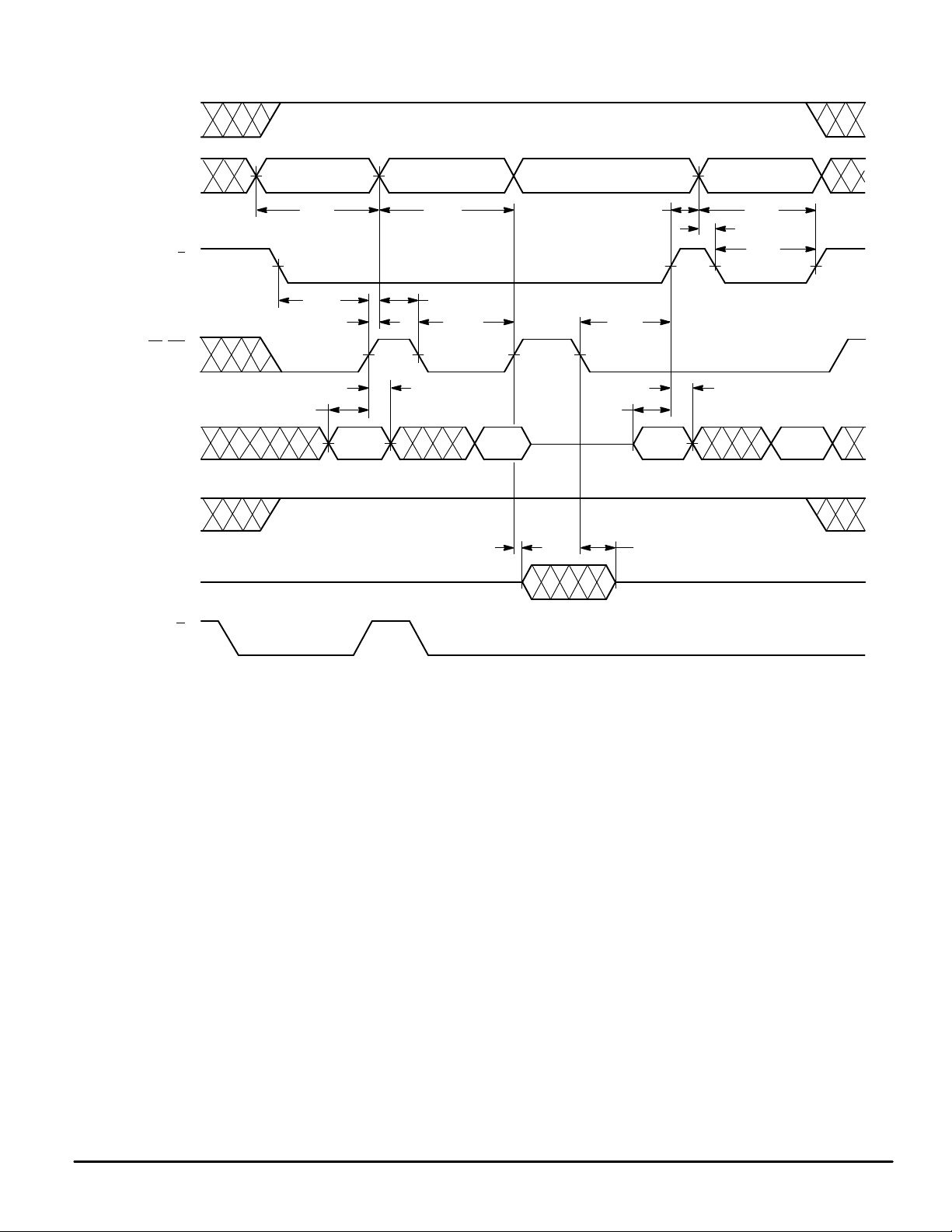
Page 10

MCM67A618
10
MOTOROLA FAST SRAM
LATCHED WRITE CYCLE TIMING (See Notes 1, 2, and 3)
MCM67A618–10 MCM67A618–12 MCM67A618–15
Parameter Symbol Min Max Min Max Min Max Unit Notes
Write Cycle Times:
Address Valid to Address Valid
t
AVAV
10 — 12 — 15 — ns 4
Setup Times:
Address Valid to End of Write
Address Valid to End of Write
E
Valid to AL Low
Address Valid to AL Low
E
Valid to AL High
Address Valid to AL High
AL High to W
Low
Address Valid to W
Low
Address Valid to E
Low
Data Valid to DL Low
Data Valid to W
High
Data Valid to E
High
DL High to W
High
DL High to E
High
t
AVWH
t
AVEH
t
EVALL
t
AVALL
t
EVALH
t
AVALH
t
ALHWL
t
AVWL
t
AVEL
t
DVDLL
t
DVWH
t
DVEH
t
DLHWH
t
DLHEH
9
9
2
2
0
0
0
0
0
2
5
5
5
5
—
—
—
—
—
—
—
—
—
—
—
—
—
—
10
10
2
2
0
0
0
0
0
2
6
6
6
6
—
—
—
—
—
—
—
—
—
—
—
—
—
—
13
13
2
2
0
0
0
0
0
2
7
7
7
7
—
—
—
—
—
—
—
—
—
—
—
—
—
—
ns
Hold Times:
AL Low to E
High
AL Low to Address Invalid
DL Low to Data Invalid
W
High to Address Invalid
E
High to Address Invalid
W
High to Data Invalid
E
High to Data Invalid
W
High to DL High
E
High to DL High
W
High to AL High
t
ALLEH
t
ALLAX
t
DLLDX
t
WHAX
t
EHAX
t
WHDX
t
EHDX
t
WHDLH
t
EHDLH
t
WHALH
2
2
2
0
0
0
0
0
0
0
—
—
—
—
—
—
—
—
—
—
2
2
2
0
0
0
0
0
0
0
—
—
—
—
—
—
—
—
—
—
3
3
3
0
0
0
0
0
0
0
—
—
—
—
—
—
—
—
—
—
ns
4
4
Write Pulse Width:
AL High to W
High
Write Pulse Width (G
Low)
Write Pulse Width (G
High)
Write Pulse Width
Enable to End of Write
Enable to End of Write
t
ALHWH
t
WLWH
t
WLWH
t
WLEH
t
ELWH
t
ELEH
9
9
8
9
9
9
—
—
—
—
—
—
10
10
9
10
10
10
—
—
—
—
—
—
13
13
12
13
13
13
—
—
—
—
—
—
ns
5
6
7
6, 7
Address Latch Pulse Width t
ALHALL
5 — 5 — 5 — ns 4
Output Buffer Control:
W
High to Output Active
W
Low to Output High–Z
t
WHQX
t
WLQZ
3
0
—
5
3
0
—
6
3
0
—
9
ns
8
8, 9
NOTES:
1. W
refers to either one or both byte write enables LW and UW.
2. A write occurs during the overlap of E
low and W low.
3. Both Write Enables must be equal to VIH for all address transitions.
4. All write cycle timing is referenced from the last valid address to the first transitioning address.
5. All latched inputs must meet the specified setup and hold times with stable logic levels for ALL falling edges of address latch (AL) and data
latch (DL).
6. If E
goes high coincident with or before W goes high the output will remain in a high impedance state.
7. If E
goes low coincident with or after W goes low the output will remain in a high impedance state.
8. Transition is measured ± 500 mV from steady–state voltage with output load of Figure 1B. This parameter is sampled and not 100% tested.
At any given voltage and temperature, t
WLQZ
is less than t
WHQX
for a given device.
9. If G
goes low coincident with or after W goes low the output will remain in a high impedance state.
Page 11

MCM67A618
11
MOTOROLA FAST SRAM
LATCHED WRITE CYCLES
AL (ADDRESS
LATCH)
Q (DATA OUT)
E
(CHIP ENABLE)
A (ADDRESS)
LW
, UW
(WRITE ENABLE)
DL
(DATA LATCH)
DATA–IN
t
ALHALL
t
AVALL
t
ALLAX
t
AVALH
t
EVALH
t
EVALL
t
ALLEH
t
AVAV
t
AVEH
t
ELEH
t
EHAX
t
ALHWH
t
ALHWL
t
WLWH
t
AVWL
t
WHALH
t
WLEH
t
AVWH
t
ELWH
t
WHAX
t
DVWH
t
WHDX
t
DLHEH
t
DVEH
t
EHDX
t
DLHWH
t
DVDLL
t
WHDLH
t
DLLDX
t
EHDLH
t
WLQZ
t
WHQX
t
AVEL
A1 A2 A3
D(A3)D(A2)D(A1) D(A4)
A4
ORDERING INFORMATION
(Order by Full Part Number)
Motorola Memory Prefix
Part Number
Full Part Numbers — MCM67A618FN10 MCM67A618FN12 MCM67A618FN15
Speed (10 = 10 ns, 12 = 12 ns, 15 = 15 ns)
Package (FN = PLCC)
MCM 67A618 XX XX
Motorola reserves the right to make changes without further notice to any products herein. Motorola makes no warranty , representation or guarantee regarding
the suitability of its products for any particular purpose, nor does Motorola assume any liability arising out of the application or use of any product or circuit,
and specifically disclaims any and all liability, including without limitation consequential or incidental damages. “T ypical” parameters can and do vary in different
applications. All operating parameters, including “T ypicals” must be validated for each customer application by customer’s technical experts. Motorola does
not convey any license under its patent rights nor the rights of others. Motorola products are not designed, intended, or authorized for use as components in
systems intended for surgical implant into the body, or other applications intended to support or sustain life, or for any other application in which the failure of
the Motorola product could create a situation where personal injury or death may occur. Should Buyer purchase or use Motorola products for any such
unintended or unauthorized application, Buyer shall indemnify and hold Motorola and its officers, employees, subsidiaries, affiliates, and distributors harmless
against all claims, costs, damages, and expenses, and reasonable attorney fees arising out of, directly or indirectly, any claim of personal injury or death
associated with such unintended or unauthorized use, even if such claim alleges that Motorola was negligent regarding the design or manufacture of the part.
Motorola and are registered trademarks of Motorola, Inc. Motorola, Inc. is an Equal Opportunity/Affirmative Action Employer.
Page 12

MCM67A618
12
MOTOROLA FAST SRAM
PACKAGE DIMENSIONS
FN PACKAGE
52–LEAD PLCC
CASE 778–02
A
B
C
E
F
G
H
J
K
R
U
V
W
X
Y
Z
G1
K1
MIN MINMAX MAX
INCHES MILLIMETERS
DIM
19.94
19.94
4.20
2.29
0.33
0.66
0.51
0.64
19.05
19.05
1.07
1.07
1.07
—
2
°
18.04
1.02
20.19
20.19
4.57
2.79
0.48
0.81
—
—
19.20
19.20
1.21
1.21
1.42
0.50
10
°
18.54
—
0.785
0.785
0.165
0.090
0.013
0.026
0.020
0.025
0.750
0.750
0.042
0.042
0.042
—
2
°
0.710
0.040
0.795
0.795
0.180
0.110
0.019
0.032
—
—
0.756
0.756
0.048
0.048
0.056
0.020
10
°
0.730
—
1.27 BSC0.050 BSC
NOTES:
1. DUE TO SPACE LIMITATION, CASE 778-02 SHALL BE
REPRESENTED BY A GENERAL (SMALLER) CASE
OUTLINE DRAWING RATHER THAN SHOWING ALL 52
LEADS.
2. DATUMS -L-, -M-, AND -N- DETERMINED WHERE TOP OF
LEAD SHOULDER EXITS PLASTIC BODY AT MOLD
PARTING LINE.
3. DIM G1, TRUE POSITION TO BE MEASURED AT DATUM -T-,
SEATING PLANE.
4. DIM R AND U DO NOT INCLUDE MOLD FLASH.
ALLOWABLE MOLD FLASH IS 0.010 (0.250) PER SIDE.
5. DIMENSIONING AND TOLERANCING PER ANSI Y14.5M,
1982.
6. CONTROLLING DIMENSION: INCH.
7. THE PACKAGE TOP MAY BE SMALLER THAN THE
PACKAGE BOTTOM BY UP TO 0.012 (0.300). DIMENSIONS
R AND U ARE DETERMINED AT THE OUTERMOST
EXTREMES OF THE PLASTIC BODY EXCLUSIVE OF MOLD
FLASH, TIE BAR BURRS, GATE BURRS AND INTERLEAD
FLASH, BUT INCLUDING ANY MISMATCH BETWEEN THE
TOP AND BOTTOM OF THE PLASTIC BODY.
8. DIMENSION H DOES NOT INCLUDE DAMBAR
PROTRUSION OR INTRUSION. THE DAMBAR
PROTRUSION(S) SHALL NOT CAUSE THE H DIMENSION
TO BE GREATER THAN 0.037 (0.940). THE DAMBAR
INTRUSION(S) SHALL NOT CAUSE THE H DIMENSION TO
BE SMALLER THAN 0.025 (0.635).
G1
VIEW S
-N-
-M-
-L-
C
E
J
G
Z
A
R
D
W
D
1
V
Y BRK
52
LEADS
ACTUAL
(NOTE 1)
52
B
U
Z
VIEW D-D
H
K1
K
VIEW S
F
G1
X
0.007 (0.180) T L
–M
SNSM
0.007 (0.180) T L
–M
SNSM
0.007 (0.180) T L
–M
SNS
M
0.007 (0.180) T L
–M
SNSM
0.007 (0.180) T L
–M
SNS
M
0.007 (0.180) T L
–M
SNSM
0.010 (0.250) T L
–M
SNSS
0.010 (0.250) T L
–M
SNSS
0.004 (0.100)
SEATING
PLANE
-T-
(NOTE 1)
52
Literature Distribution Centers:
USA/EUROPE: Motorola Literature Distribution; P .O. Box 20912; Phoenix, Arizona 85036.
JAPAN: Nippon Motorola Ltd.; 4–32–1, Nishi–Gotanda, Shinagawa–ku, Tokyo 141, Japan.
ASIA PACIFIC: Motorola Semiconductors H.K. Ltd.; Silicon Harbour Center, No. 2 Dai King Street, Tai Po Industrial Estate, Tai Po, N.T., Hong Kong.
MCM67A618/D
*MCM67A618/D*
◊
CODELINE TO BE PLACED HERE
 Loading...