

Datasheet MCM44B256BSG15, MCM44B256BSG17, MCM44A256BSG17, MCM44A256BSG12, MCM44A256BSG15 Datasheet (Motorola)
...Page 1
MCM44256B SERIES
1
MOTOROLA FAST SRAM
4MB R4000 Secondary Cache Fast
Static RAM Module Set
Four MCM44256B modules comprise a full 4 MB of secondary cache for the
R4000 processor. Each module contains nine MCM6729DWJ fast static RAMs
for a cache data size of 256K x 36. The tag portion, dependent on word line size,
contains either two MCM6729DWJ or one MCM6726DWJ fast static RAMs. All
input signals, except A0 and WE
are buffered using 74FBT2827 drivers with se-
ries 25 Ω resistors.
The MCM6729DWJ and MCM6726DWJ are fabricated using high–performance silicon–gate BiCMOS technology. Static design eliminates the need for
internal clocks or timing strobes.
All 4MB R4000 supported secondary cache options are available.
• Single 5 V ± 10% Power Supply
• All Inputs and Outputs are TTL Compatible
• Fast Module Access Time: 12/15/17 ns
• Zero Wait–State Operation
• Unified or Split Secondary Cache is Supported
• Word Line Sizes of 4, 8, 16, and 32 are Available (See Ordering
Information for Details)
• Decoupling Capacitors are Used for Each Fast Static RAM and Buffer ,
Along with Bulk Capacitance for Maximum Noise Immunity
• High Quality Multi–Layer FR4 PWB with Separate Power and Ground
Planes
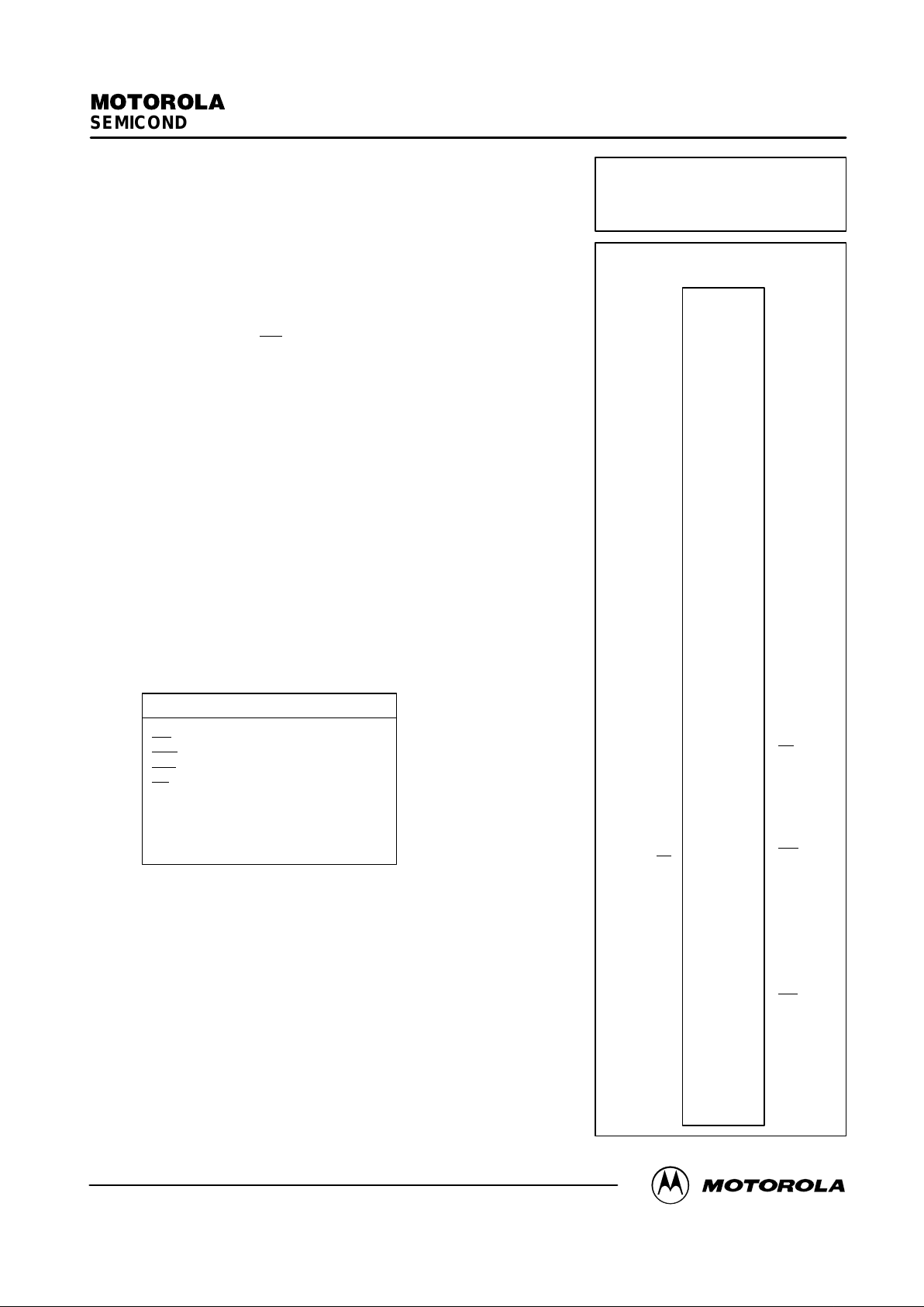
PIN NAMES
A0 – A17 Address Inputs. . . . . . . . . . . . . . . .
WE
Write Enable. . . . . . . . . . . . . . . . . . . . . . .
DCS
Data Enable. . . . . . . . . . . . . . . . . . . . . .
TCS
Tag Enable. . . . . . . . . . . . . . . . . . . . . . .
OE
Output Enable. . . . . . . . . . . . . . . . . . . . .
DQ0 – DQ35 Data Input / Output. . . . . . . . .
TDQ0 – TDQ7 TAG Data Input / Output. . .
V
CC
+ 5 V Power Supply. . . . . . . . . . . . . . . .
V
SS
Ground. . . . . . . . . . . . . . . . . . . . . . . . . .
For proper operation of the device, VSS must
be connected to ground.
Order this document
by MCM44256B/D
MOTOROLA
SEMICONDUCTOR TECHNICAL DATA
PIN ASSIGNMENT
80 LEAD SIMM — TOP VIEW
MCM44256B
Series
2
DQ5
V
SS
DQ8
DQ10
DQ12
DQ14
DQ15
DQ17
DQ19
DQ21
V
SS
DQ23
DQ25
DQ27
V
SS
DQ0
DQ2
DQ4
DQ6
DQ9
DQ11
DQ13
V
SS
DQ16
DQ18
DQ20
DQ22
V
CC
DQ28
DQ7
19
21
23
25
27
29
1
3
5
7
9
11
13
15
17
20
22
24
26
28
30
32
4
6
8
10
12
14
16
18
31
DQ3
33
35
37
34
36
38
40
39
DQ31
V
SS
DQ26
DQ24
DQ34 42
A0
A2
A4
A6
V
CC
OE
A8
A10
V
SS
A13
A15
A17
TDQ0
TDQ1
DQ33
DQ35
WE
A1
A3
V
SS
DCS
A7
A9
A11
A12
A14
A16
TCS
TDQ4
A5
59
61
63
65
67
69
41
43
45
47
49
51
53
55
57
60
62
64
66
68
70
72
44
46
48
50
52
54
56
58
71
V
SS
73
75
77
74
76
78
80
79 V
CC
TDQ6
TDQ2
V
SS
DQ29
DQ30
DQ32
DQ1
TDQ3
TDQ5
TDQ7
V
SS
V
CC
11/19/97
Motorola, Inc. 1997
Page 2
MCM44256B SERIES
2
MOTOROLA FAST SRAM
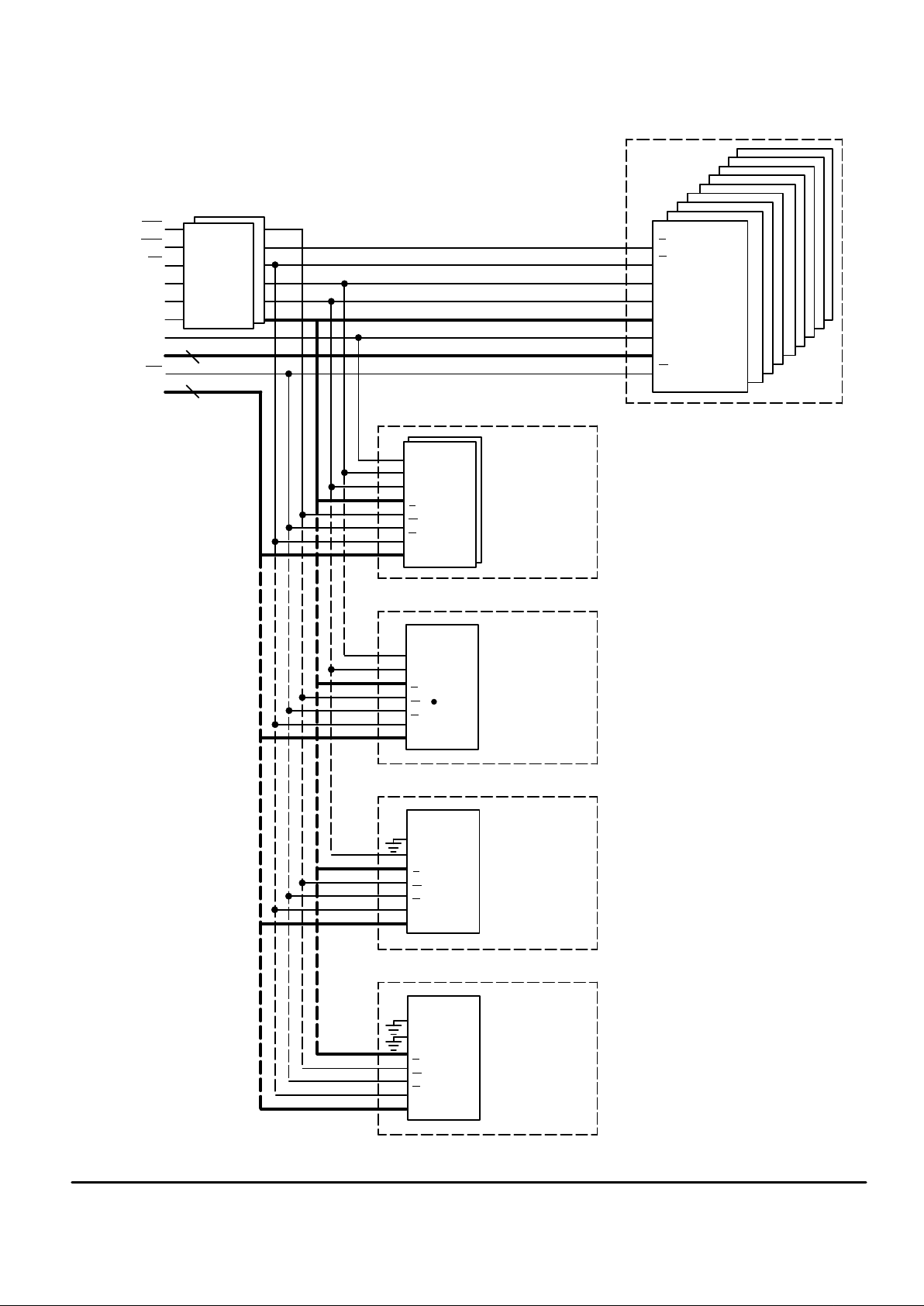
BLOCK DIAGRAM
A0
DQ0 – DQ3
W
256K x 4
E
G
A1
A2
A3 – A17
A3 – A17
A0
DQ0 – DQ35
TCS
DCS
OE
A1
A2
WE
TDQ0 – TDQ7
74FBT2827
DRIVER
4 WORD
LINE SIZE
256K x 36 CACHE
TAG OPTIONS:
36
8
W
G
DQ0 – DQ3
A0
A1
A2
A3 – A17
E
256K x 8
TAG
8 WORD
LINE SIZE
128K x 8
TAG
(A0 NOT USED)
16 WORD
LINE SIZE
64K x 8
TAG
(A0, A1 NOT USED)
32 WORD
LINE SIZE
32K x 8
TAG
(A0, A1, A2 NOT USED)
W
G
DQ0 – DQ7
A0
A1
A2 – A16
E
W
G
DQ0 – DQ7
A0
A1
A2 – A16
E
W
G
DQ0 – DQ7
A0
A1
A2 – A16
E
256K x 4
128K x 8
128K x 8
128K x 8
Page 3
MCM44256B SERIES
3
MOTOROLA FAST SRAM
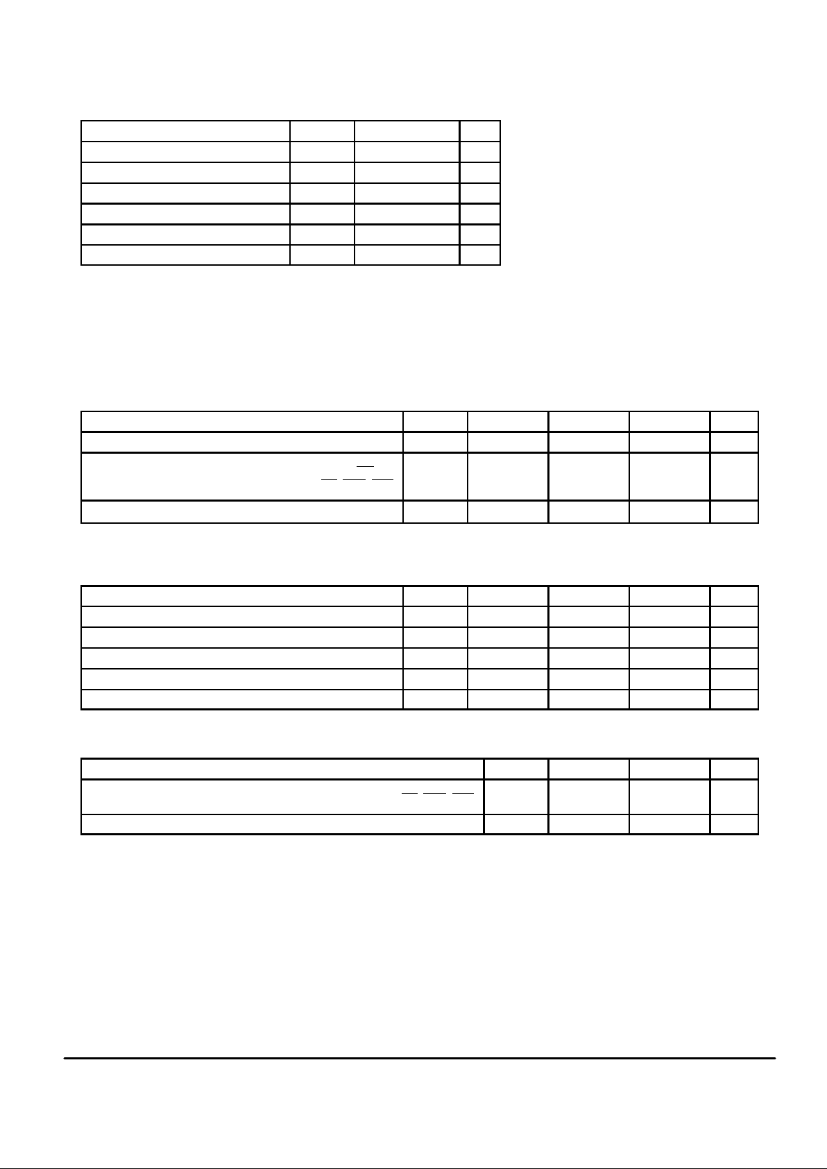
ABSOLUTE MAXIMUM RATINGS (Voltages Referenced to V
SS
= 0 V)
Rating
Symbol Value Unit
Power Supply Voltage V
CC
– 0.5 to 7.0 V
Voltage Relative to V
SS
Vin, V
out
– 0.5 to VCC + 0.5 V
Output Current (per I/O) I
out
± 30 mA
Power Dissipation P
D
10 W
Temperature Under Bias T
bias
– 10 to + 85 °C
Storage Temperature T
stg
– 25 to +125 °C
NOTE: Permanent device damage may occur if ABSOLUTE MAXIMUM RATINGS are
exceeded. Functional operation should be restricted to RECOMMENDED OPERATING CONDITIONS. Exposure to higher than recommended voltages for
extended periods of time could affect device reliability.
DC OPERA TING CONDITIONS AND CHARACTERISTICS
(VCC = 5.0 V ± 10%, TA = 0 to + 70°C, Unless Otherwise Noted)
RECOMMENDED OPERATING CONDITIONS
(Voltages Referenced to VSS = 0 V)
Parameter
Symbol Min Typ Max Unit
Supply Voltage (Operating Voltage Range) V
CC
4.5 5.0 5.5 V
Input High Voltage
(DQ0 – 35, TDQ0 – 7, WE
, A0)
(A1 – A17, OE
, DCS, TCS)
V
IH
2.2
2.0
—
—
VCC + 0.3 V*
VCC + 0.3 V*
V
Input Low Voltage V
IL
– 0.5**
— 0.8 V
*VIH (max) = VCC + 0.3 V dc; VIH (max) = VCC + 2 V ac (pulse width ≤ 20 ns).
**VIL (min) = – 3.0 V ac (pulse width ≤ 20 ns).
DC CHARACTERISTICS
Parameter Symbol Min Typ Max Unit
Input Leakage Current (All Inputs, Vin = 0 to VCC) I
lkg(I)
± 10 µA
Output Leakage Current (G, xCS = VIH, V
out
= 0 to VCC) Ilkg(O) ± 10 µA
AC Supply Current (G, xCS = VIL, I
out
= 0 mA) I
CCA
1750 mA
Output Low Voltage (IOL = + 8 mA) V
OL
0.4 V
OUtput High Voltage (IOH = – 4.0 mA) V
OH
2.4 V
NOTE: Good decoupling of the local power supply should always be used.
CAPACITANCE (f = 1.0 MHz, dV = 3.0 V, T
A
= 25°C, Periodically Sampled Rather Than 100% Tested)
Parameter
Symbol Typ Max Unit
Input Capacitance (A0, WE)
(A1 – A17, OE
, DCS, TCS)
C
in
C
in
110
10
pF
pF
Input/Output Capacitance C
out
10 pF
This devices on this module contain circuitry
to protect the inputs against damage due to
high static voltages or electric fields; however,
it is advised that normal precautions be taken
to avoid application of any voltage higher than
maximum rated voltages to these high–impedance circuits.
These BiCMOS memory circuits have been
designed to meet the dc and ac specifications
shown in the tables, after thermal equilibrium
has been established. The module is in a test
socket or mounted on a printed circuit board
and transverse air flow of at least 500 linear feet
per minute is maintained.
Page 4

MCM44256B SERIES
4
MOTOROLA FAST SRAM
AC OPERA TING CONDITIONS AND CHARACTERISTICS
(VCC = 5.0 V ± 10%, TA = 0 to + 70°C, Unless Otherwise Noted)
Input Timing Measurement Reference Level 1.5 V. . . . . . . . . . . . . . .
Input Pulse Levels 0 to 3.0 V. . . . . . . . . . . . . . . . . . . . . . . . . . . . . . . . .
Input Rise/Fall Time 1 V/ns (20% to 80%). . . . . . . . . . . . . . . . . . . . . .
Output Timing Measurement Reference Level 1.5 V. . . . . . . . . . . . .
Output Load See Figure 1. . . . . . . . . . . . . . . . . . . . . . . . . . . . . . . . . . . .
READ CYCLE (See Notes 1 and 2)
–12 –15 –17
Parameter Symbol
Min Max Min Max Min Max
Unit Notes
Address Access Time t
AVQV
— 12 — 15 — 17 ns
A0 Access Time t
A0AQV
— 10 — 12 — 14 ns
Data/Tag Enable Access Time t
ELQV
— 12 — 15 — 17 ns
Output Enable Access Time t
GLQV
— 9 — 10 — 11 ns
Output Hold from Address Change t
AXQX
4 — 4 — 4 — ns
Output Hold from A0 Change t
A0XQX
4 — 4 — 4 — ns
Data/Tag Enable Low to Output Active t
ELQX
2 — 2 — 2 — ns 3, 4
Data/Tag Enable High to Output High–Z t
EHQZ
1 9 1 10 1 11 ns 3, 4
Output Enable Low to Output Active t
GLQX
1 — 1 — 1 — ns 3, 4
Output Enable High to Output High–Z t
GHQZ
1 9 1 10 1 11 ns 3, 4
NOTES:
1. WE
is high for read cycle.
2. Enable timings are the same for both DCS
and TCS.
3. Transition is measured 200 mV from steady–state voltage.
4. This parameter is sampled and not 100% tested.
The table of timing values shows either a minimum
or a maximum limit for each parameter. Input requirements are specified from the external system point of
view. Thus, address setup time is shown as a minimum since the system must supply at least that much
time. On the other hand, responses from the memory
are specified from the device point of view. Thus, the
access time is shown as a maximum since the device
never provides data later than that time.
TIMING LIMITS
OUTPUT
Z0 = 50
Ω
RL = 50
Ω
VL = 1.5 V
Figure 1. AC Test Load
Page 5

MCM44256B SERIES
5
MOTOROLA FAST SRAM
Q (DATA OUT)
A1 – A17
DATA VALIDPREVIOUS DATA VALID
A0
t
AVQV
t
A0VQV
t
A0XQX
t
AXQX
NOTE: Module is continuously selected (DCS or TCS = VIL, OE = VIL).
READ CYCLE 1 (See Note)
t
EHQZ
DATA VALID
t
GHQZ
t
ELQX
t
ELQV
OE (OUTPUT ENABLE)
Q (DATA OUT)
A1 – A17
t
GLQX
t
GLQV
DCS/TCS
(DATA/TAG ENABLE)
t
AVQV
t
A0VQV
A0
NOTE: Address valid prior to or coincident with DCS or TCS going low.
READ CYCLE 2 (See Note)
Page 6

MCM44256B SERIES
6
MOTOROLA FAST SRAM
WRITE CYCLE 1 (WE Controlled, See Notes 1 and 2)
–12 –15 –17
Parameter Symbol
Min Max Min Max Min Max
Unit Notes
Address Setup Time t
AVWL
5 — 5 — 5 — ns
A0 Setup Time t
A0VWL
0 — 0 — 0 — ns
Address Valid to End of W rite t
AVWH
12 — 15 — 17 — ns
A0 Valid to End of W rite t
A0VWH
10 — 12 — 14 — ns
Write Pulse Width t
WLWH
,
t
WLEH
7 — 10 — 12 — ns
Data Valid to End of W rite t
DVWH
6 — 7 — 8 — ns
Data Hold Time t
WHDX
0 — 0 — 0 — ns
Write Low to Data High–Z t
WLQZ
0 4 0 5 0 6 ns 3, 4
Write High to Output Active t
WHQX
3 — 3 — 3 — ns 3, 4
Write Recovery Time t
WHAX
0 — 0 — 0 — ns
Write Recovery Time — A0 t
WHA0X
0 — 0 — 0 — ns
NOTES:
1. A write occurs during the overlap of DCS
or TCS low and WE low.
2. Enable timings are the same for both DCS
and TCS.
3. Transition is measured 200 mV from steady–state voltage.
4. This parameter is sampled and not 100% tested.
t
A0VWL
DATA VALID
t
AVWH
t
WHDX
t
WLQZ
t
WHQX
HIGH–Z
A1 – A17
WE
(WRITE ENABLE)
DCS
/TCS
(DATA/TAG ENABLE)
Q (DATA OUT)
D (DATA IN)
t
WLEH
t
WHAX
t
AVWL
A0
t
WLWH
t
DVWH
t
WHA0X
t
A0VWH
HIGH–Z
WRITE CYCLE 1
Page 7

MCM44256B SERIES
7
MOTOROLA FAST SRAM
WRITE CYCLE 2 (DCS or TCS Controlled, See Notes 1 and 2)
–12 –15 –17
Parameter Symbol
Min Max Min Max Min Max
Unit Notes
Address Setup Time t
AVEL
0 — 0 — 0 — ns
A0 Setup Time t
A0VEL
0 — 0 — 0 — ns
Address Valid to End of W rite t
AVEH
12 — 15 — 17 — ns
A0 Valid to End of W rite t
A0VEH
10 — 12 — 14 — ns
Data/Tag Enable to End of Write t
ELEH,
t
ELWH
12 — 15 — 17 — ns
Data Valid to End of W rite t
DVEH
6 — 7 — 8 — ns
Data Hold Time t
EHDX
5 — 5 — 5 — ns
Write Recovery Time t
EHAX
5 — 5 — 5 — ns
Write Recovery Time — A0 t
EHA0X
5 — 5 — 5 — ns
NOTES:
1. A write occurs during the overlap of DCS
or TCS low and WE low.
2. Enable timings are the same for both DCS
and TCS.
t
EHDX
t
DVEH
t
EHAX
t
ELWH
t
ELEH
t
AVEL
DATA VALID
HIGH–Z
WE
(WRITE ENABLE)
DCS/TCS
(DATA/TAG ENABLE)
Q (DATA OUT)
D (DATA IN)
A1 – A17
t
AVEH
A0
t
EHA0X
t
A0VEL
t
A0VEH
WRITE CYCLE 2
Page 8

MCM44256B SERIES
8
MOTOROLA FAST SRAM
MCM 44X256B XX XX
Motorola Memory Prefix
Part Number
Speed (12 = 12 ns, 15 = 15 ns, 17 = 17 ns)
Package (SG = Gold Pad SIMM)
ORDERING INFORMATION
(Order by Full Part Number)
Part Number Unified/Split Word Line Size TAG Depth
MCM44A256B Unified/Split 4 256K
MCM44B256B Unified/Split 8 128K
MCM44C256B Unified/Split 16 64K
MCM44D256B Unified/Split 32 32K
Motorola reserves the right to make changes without further notice to any products herein. Motorola makes no warranty , representation or guarantee regarding
the suitability of its products for any particular purpose, nor does Motorola assume any liability arising out of the application or use of any product or circuit, and
specifically disclaims any and all liability, including without limitation consequential or incidental damages. “T ypical” parameters which may be provided in Motorola
data sheets and/or specifications can and do vary in different applications and actual performance may vary over time. All operating parameters, including “Typicals”
must be validated for each customer application by customer’s technical experts. Motorola does not convey any license under its patent rights nor the rights of
others. Motorola products are not designed, intended, or authorized for use as components in systems intended for surgical implant into the body, or other
applications intended to support or sustain life, or for any other application in which the failure of the Motorola product could create a situation where personal injury
or death may occur. Should Buyer purchase or use Motorola products for any such unintended or unauthorized application, Buyer shall indemnify and hold Motorola
and its officers, employees, subsidiaries, affiliates, and distributors harmless against all claims, costs, damages, and expenses, and reasonable attorney fees
arising out of, directly or indirectly, any claim of personal injury or death associated with such unintended or unauthorized use, even if such claim alleges that
Motorola was negligent regarding the design or manufacture of the part. Motorola and are registered trademarks of Motorola, Inc. Motorola, Inc. is an Equal
Opportunity/Affirmative Action Employer.
Mfax is a trademark of Motorola, Inc.
How to reach us:
USA/EUROPE/ Locations Not Listed: Motorola Literature Distribution; JAP AN: Nippon Motorola Ltd.: SPD, Strategic Planning Office, 141,
P.O. B o x 5405, Denver , Colorado, 80217. 1-303-675-2140 or 1-800-441-2447 4-32-1 Nishi-Gotanda, Shagawa-ku, T okyo, Japan. 03-5487-8488
Mfax: RMF AX0@email.sps.mot.com – TOUCHTONE 1-602-244-6609 ASIA/P ACIFIC: Motorola Semiconductors H.K. Ltd.; 8B Tai Ping Industrial Park,
Motorola Fax Back System – US & Canada ONL Y 1-800-774-1848 51 Ting Kok Road, Tai Po, N.T., Hong Kong. 852-26629298
– http://sps.motorola.com/mfax/
HOME PAGE: http://motorola.com/sps/ CUSTOMER FOCUS CENTER: 1-800-521-6274
MCM44256B/D
◊
 Loading...