

Page 1
MOTOROLA
SEMICONDUCTOR TECHNICAL DATA
Advance Information
1MB and 2MB Synchronous
Order this document
by MCM36F8/D
MCM36F8
MCM36F9
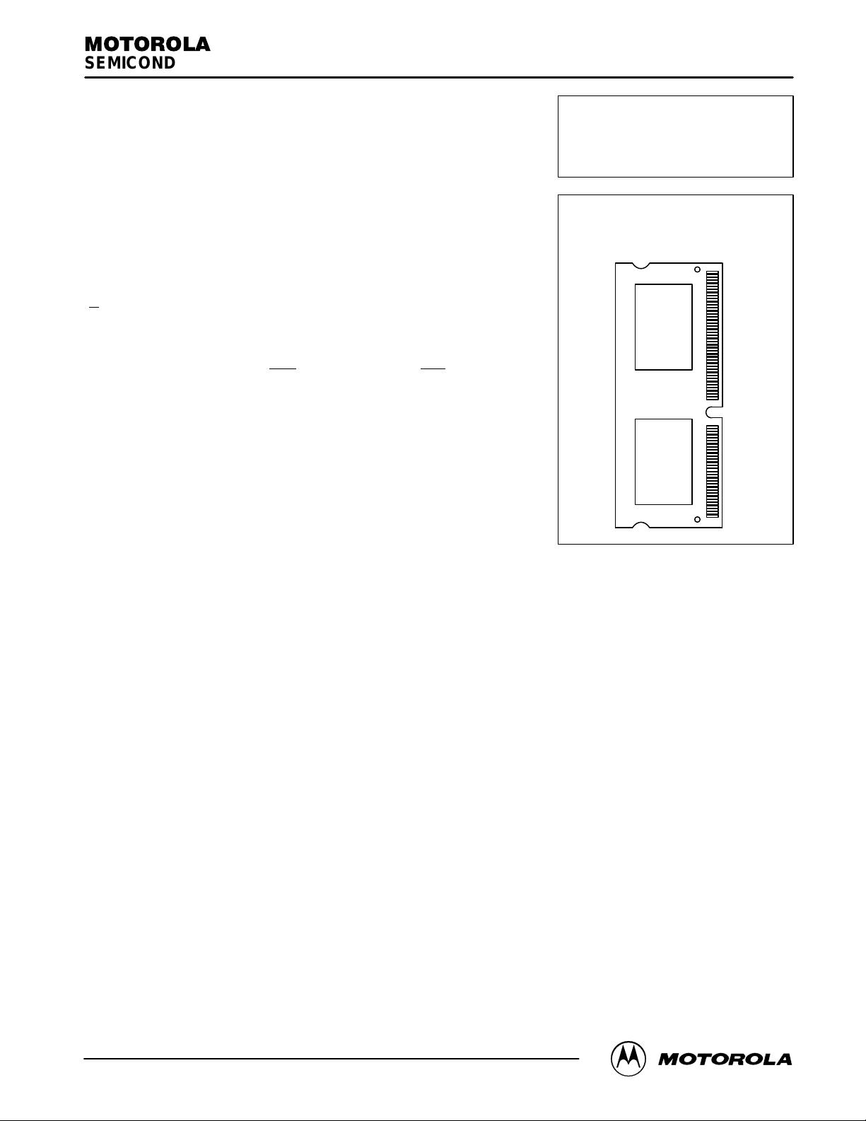
Fast Static RAM Module
The MCM36F8 (1MB) is configured as 256K x 36 bits and the MCM36F9 (2MB)
is configured as 512K x 36 bits. Both are packaged in a 144–pin dual–in–line
memory module (DIMM). Each module uses Motorola’s 3.3 V 256K x 18 bit flow–
through BurstRAMs.
Address (A), data inputs (DQ, DP), and all control signals except output enable
) are clock (K) controlled through positive–edge–triggered noninverting
(G
registers.
Write cycles are internally self–timed and initiated by the rising edge of the
clock (K) input. This feature provides increased timing flexibility for incoming
signals. Synchronous byte write (BWx
to either individual bytes or to both bytes.
• Single 3.3 V + 10%, – 5% Power Supply
• Multiple Clock Pins for Reduced Loading
• All Inputs and Outputs are L VTTL Compatible
• Byte Write and Global Write Capability
• Fast SRAM Access Times: 10 ns
• Berg Connector, Part Number: 61178–31844
• 144–Pin DIMM Module
) and global byte write (WE) allows writes
144–LEAD DIMM
CASE 1154–01
TOP VIEW
143
61
59
1
This document contains information on a new product. Specifications and information herein are subject to change without notice.
2/10/98
Motorola, Inc. 1998
MOTOROLA FAST SRAM
MCM36F8•MCM36F9
1
Page 2
MCM36F8 BLOCK DIAGRAM
E0
G0
A0 – A17
ADSP
BW0
BW1
K0
V
DD
WE
V
SS
DQ0 – DQ7
DP0
DQ8 – DQ15
DP1
256K x 18
SE1
G
A0 – A17
ADSC
SBa
SBb
K
SE2
ADV
ADSP
SGW
SW
LBO
SE3
DQa0 – DQa7
DQa8
DQb0 – DQb7
DQb8
DQ16 – DQ23
DQ24 – DQ31
DP2
DP3
BW2
BW3
K1
256K x 18
SE1
G
A0 – A17
ADSC
SBa
SBb
K
SE2
ADV
ADSP
SGW
SW
LBO
SE3
DQa0 – DQa7
DQa8
DQb0 – DQb7
DQb8
PD1 = GND
PD0 = GND
MCM36F8•MCM36F9
2
MOTOROLA FAST SRAM
Page 3
MCM36F9 BLOCK DIAGRAM
K0
E0
G0
A0 – A17
ADSP
BW0
BW1
WE
V
DD
V
SS
DQ0 – DQ7
DP0
DQ8 – DQ15
DP1
V
DD
V
SS
K2
E1
G1
256K x 18
K
SE1
G
A0 – A17
ADSC
SBa
SBb
SGW
DQa0 – DQa7
DQa8
DQb0 – DQb7
DQb8
SE2
ADV
ADSP
SW
LBO
SE3
DQ16 – DQ23
DQ24 – DQ31
256K x 18
A0 – A17
ADSC
SBa
SBb
SGW
DQb8
DQb0 – DQb7
DQa8
DQa0 – DQa7
SE2
ADV
ADSP
SW
LBO
SE3
K
SE1
G
DP2
DP3
K1
BW2
BW3
K3
256K x 18
K
SE1
G
A0 – A17
ADSC
SBa
SBb
SGW
DQa0 – DQa7
DQa8
DQb0 – DQb7
DQb8
SE2
ADV
ADSP
SW
LBO
SE3
256K x 18
A0 – A17
ADSC
SBa
SBb
SGW
DQb8
DQb0 – DQb7
DQa8
DQa0 – DQa7
SE2
ADV
ADSP
SW
LBO
SE3
K
SE1
G
PD1 = NC
PD0 = GND
MOTOROLA FAST SRAM
MCM36F8•MCM36F9
3
Page 4
PIN ASSIGNMENT
144–LEAD DIMM
TOP VIEW
V
SS
A0
A2
A4
V
DD
NC
NC
V
SS
A6
A8
A10
NC
V
DD
A12
A14
A16
V
SS
PD0
V
SS
BW0
E0
V
SS
K1
V
SS
DQ0
V
DD
DQ2
DQ4
DQ6
V
SS
V
DD
DQ8
DQ10
V
SS
DQ12
DQ14
DP0
NC
NC
V
SS
WE
NC
V
DD
NC
NC
NC
V
DD
NC
NC
NC
V
SS
BW2
E1
V
DD
DQ16
DQ18
NC
NC
NC
V
SS
K3
V
SS
DQ20
V
SS
DQ22
DQ24
DQ26
DQ28
V
DD
DQ30
DP2
V
SS
1
3
5
7
9
11
13
15
17
19
21
23
25
27
29
31
33
35
37
39
41
43
45
47
49
51
53
55
57
59
61
63
65
67
69
71
73
75
77
79
81
83
85
87
89
91
93
95
97
99
101
103
105
107
109
111
113
115
117
119
121
123
125
127
129
131
133
135
137
139
141
143
10
12
14
16
18
20
22
24
26
28
30
32
34
36
38
40
42
44
46
48
50
52
54
56
58
60
62
64
66
68
70
72
74
76
78
80
82
84
86
88
90
92
94
96
98
100
102
104
106
108
110
112
114
116
118
120
122
124
126
128
130
132
134
136
138
140
142
144
2
4
6
8
V
SS
A1
A3
A5
V
DD
NC
NC
V
SS
A7
A9
A11
NC
V
DD
A13
A15
A17
V
SS
PD1
V
SS
BW1
G0
V
SS
K0
V
SS
DQ1
V
DD
DQ3
DQ5
DQ7
V
SS
V
DD
DQ9
DQ11
V
SS
DQ13
DQ15
DP1
NC
NC
V
SS
ADSP
NC
V
DD
NC
NC
NC
V
DD
NC
NC
NC
V
SS
BW3
G1
V
DD
DQ17
DQ19
NC
NC
NC
V
SS
K2
V
SS
DQ21
V
SS
DQ23
DQ25
DQ27
DQ29
V
DD
DQ31
DP3
V
SS
MCM36F8•MCM36F9
4
MOTOROLA FAST SRAM
Page 5

PIN DESCRIPTIONS
Pin Locations Symbol
3, 4, 5, 6, 7, 8, 17, 18, 19, 20,
21, 22, 27, 28, 29, 30, 31, 32
82 ADSP Input Synchronous Addresss Status Controller: Initiates read, write, or
39, 40, 103, 104 BW0 – BW3 Input Synchronous Byte Write Inputs: x refers to the byte being written
73, 74, 141, 142 DP0 – DP3 Synchronous Parity Data Inputs/Outputs.
(a) 49, 50, 53, 54, 55, 56, 57, 58,
(b) 63, 64, 65, 66, 69, 70, 71, 72
(c) 109, 110, 111, 112, 125, 126, 129, 130
(d) 131, 132, 133, 134, 135, 136, 139, 140
41, 105 E0, E1 Input Synchronous Chip Enable: Active low to enable chip. Negated
42, 106 G0, G1 Input Asynchronous Output Enable Input.
46, 45, 122, 121 K0 – K3 Input Clock: This signal registers the address, data in, and all control
35, 36 PD0, PD1 Output Presence Detect Bits.
81 WE Input Synchronous Global Write: This signal writes all bytes
9, 10, 25, 26, 51, 52,
61, 62, 85, 86, 93,
94, 107, 108, 137, 138
1, 2, 15, 16, 33, 34, 37, 38, 43, 44, 47, 48,
59, 60, 67, 68, 79, 80, 101, 102, 119, 120,
123, 124, 127, 128, 143, 144
11, 12, 13, 14, 23, 24,
75, 76, 77, 78, 83, 84,
87, 88, 89, 90, 91, 92, 95,
96, 97, 98, 99, 100, 113,
114, 115, 116, 117, 118
Type Description
A0 – A17 Input Synchronous Address Inputs: These inputs are registered and
DQ0 – DQ31 I/O Synchronous Data Inputs/Outputs.
V
DD
V
SS
NC — No Connection: There is no connection to the chip.
Supply Power Supply: 3.3 V + 10%, – 5%.
Supply Ground.
must meet setup and hold times.
chip deselect cycle.
(byte a, b, c, d). WE
high — deselects chip when ADSP
signals except G
regardless of the status of the BWx
signals SBx
overrides BWx.
.
are being used, tie this pin high.
is asserted.
signals. If only byte write
MOTOROLA FAST SRAM
MCM36F8•MCM36F9
5
Page 6

TRUTH TABLE (See Notes 1 through 4)
Next Cycle Address Used Ex ADSP Gx DQx WRITE2,
Deselect None 1 0 X High–Z X
Begin Read External 0 0 0 DQ Read
Read Current X 1 1 High–Z Read
Read Current X 1 0 DQ Read
Begin Write External 0 0 X High–Z Write
Write Current X 1 X High–Z Write
NOTES:
1. X = don’t care, 1 = logic high, 0 = logic low.
2. Write is defined as either any BWx
3. Gx
is an asynchronous signal and is not sampled by the clock K. Gx drives the bus immediately (t
4. On write cycles that follow read cycles, Gx
must also remain negated at the completion of the write cycle to ensure proper write data hold times.
or WE low.
must be negated prior to the start of the write cycle to ensure proper write data setup times. Gx
) following Gx going low.
GLQX
4
ABSOLUTE MAXIMUM RATINGS (Voltages Referenced to V
Rating
Power Supply Voltage V
Voltage Relative to V
Output Current (per I/O) I
Temperature Under Bias T
Storage Temperature T
NOTE: Permanent device damage may occur if ABSOLUTE MAXIMUM RATINGS are
exceeded. Functional operation should be restricted to RECOMMENDED OPERATING CONDITIONS. Exposure to higher than recommended voltages for
extended periods of time could affect device reliability.
SS
Symbol Value Unit
DD
Vin, V
out
bias
stg
– 0.5 to VDD + 0.5 V
out
= 0 V)
SS
– 0.5 to + 4.6 V
± 20 mA
– 10 to + 85 °C
– 55 to + 125 °C
This device contains circuitry to protect the
inputs against damage due to high static voltages or electric fields; however, it is advised
that normal precautions be taken to avoid
application of any voltage higher than maximum rated voltages to this high–impedance
circuit.
This BiCMOS memory circuit has been
designed to meet the dc and ac specifications
shown in the tables, after thermal equilibrium
has been established.
This device contains circuitry that will
ensure the output devices are in High–Z at
power up.
MCM36F8•MCM36F9
6
MOTOROLA FAST SRAM
Page 7

DC OPERA TING CONDITIONS AND CHARACTERISTICS
(VDD = 3.3 V + 10%, – 5%, TA = 0 to 70°C, Unless Otherwise Noted)
RECOMMENDED OPERATING CONDITIONS
Parameter
Supply Voltage V
Input High Voltage V
Input Low Voltage V
*VIL ≥ – 2.0 V for t ≤ t
KHKH
/2.
(Voltages Referenced to VSS = 0 V)
Symbol Min Typ Max Unit
DD
IH
IL
3.135 3.3 3.6 V
2.0 — VDD + 0.5 V
– 0.5* — 0.8 V
DC CHARACTERISTICS
Parameter Symbol Min Max Unit
Input Leakage Current (0 V ≤ Vin ≤ VDD) I
Output Leakage Current (0 V ≤ Vin ≤ VDD) I
Output Low Voltage (IOL = + 8.0 mA) V
Output High Voltage (IOH = – 4.0 mA) V
lkg(I)
lkg(O)
OL
OH
— ± 1.0 µA
— ± 1.0 µA
— 0.4 V
2.4 — V
POWER SUPPLY CURRENTS
Parameter Symbol Min Max Unit Notes
AC Supply Current (Device Selected, MCM36F8DG10
All Outputs Open, Cycle Time ≥ t
CMOS Standby Supply Current (Deselected, MCM36F8DG10
Clock (K) Cycle Time ≥ t
at CMOS Levels Vin ≤ VSS + 0.2 V or ≥ VDD – 0.2 V)
Clock Running Supply Current (Deselected, MCM36F8DG10
Clock (K) Cycle Time ≥ t
Held to Static CMOS Levels Vin ≤ VSS + 0.2 V
or ≥ VDD – 0.2 V)
NOTES:
1. Reference AC Operating Conditions and Characteristics for input and timing (VIH/VIL, tr/tf, pulse level 0 to 3.0 V, VIH = 3.0 V).
2. All addresses transition simultaneously low (LSB) and then high (HSB).
3. Data states are all zero.
4. Device in deselected mode as defined by the Truth Table.
, All Inputs Toggling MCM36F9DG10
KHKH
, All Other Inputs MCM36F9DG10
KHKH
min) MCM36F9DG10
KHKH
I
DDA
I
SB1
I
SB2
— 550
860
— 310
620
— 190
380
mA 1, 2, 3
mA
mA 4
MCM36F8 CAPACITANCE (f = 1.0 MHz, dV = 3.0 V, T
Parameter
Input Capacitance BWx, K
I/O Capacitance C
MCM36F9 CAPACITANCE (f = 1.0 MHz, dV = 3.0 V, T
Parameter Symbol Typ Max Unit
Input Capacitance K
I/O Capacitance C
= 0 to 70°C, Periodically Sampled Rather Than 100% Tested)
A
Other Inputs
= 0 to 70 °C, Periodically Sampled Rather Than 100% Tested)
A
Addr, ADSP
, WE
Other Inputs
MOTOROLA FAST SRAM
Symbol Typ Max Unit
C
in
I/O
C
in
I/O
—
—
— 13 pF
—
—
—
— 21 pF
10
15
10
25
15
pF
pF
MCM36F8•MCM36F9
7
Page 8

AC OPERA TING CONDITIONS AND CHARACTERISTICS
(VDD = 3.3 V + 10%, – 5%, TA = 0 to 70°C, Unless Otherwise Noted)
Input Timing Measurement Reference Level 1.25 V. . . . . . . . . . . . . .
Input Pulse Levels 0 to 2.5 V. . . . . . . . . . . . . . . . . . . . . . . . . . . . . . . . .
Input Rise/Fall Time 1 V/ns (20 to 80%). . . . . . . . . . . . . . . . . . . . . . .
Output Timing Reference Level 1.25 V. . . . . . . . . . . . . . . . . . . . . . . . .
Output Load See Figure 1 Unless Otherwise Noted. . . . . . . . . . . . . .
DATA RAM READ/WRITE CYCLE TIMING (See Notes 1, 2, 3, and 4)
Parameter Symbol
Cycle Time t
Clock Access Time t
Output Enable to Output Valid t
Clock High to Output Active t
Clock High to Output Change t
Output Enable to Output Active t
Output Disable to Q High–Z t
Clock High to Q High–Z t
Clock High Pulse Width t
Clock Low Pulse Width t
Setup Times: Address
Hold Times: Address
NOTES:
1. Write is defined as either any BWx
2. Chip Enable is defined as E0
3. All read and write cycle timings are referenced from K0 or G0
4. G0
is a don’t care after write cycle begins. To prevent bus contention, G0 should be negated prior to start of write cycle.
5. This parameter is sampled and not 100% tested.
6. Measured at ± 200 mV from steady state.
and SW low or WE is low.
low, SE2 high, and SE3 low whenever ADSP or ADSC is asserted.
ADSP
ADSP
Data In
Write
Chip Enable
, ADSC, ADV
Data In
Write
Chip Enable
.
KHKH
KHQV
GLQV
KHQX1
KHQX2
GLQX
GHQZ
KHQZ
KHKL
KLKH
t
AVKH
t
ADKH
t
DVKH
t
WVKH
t
EVKH
t
KHAX
t
KHADX
t
KHDX
t
KHWX
t
KHEX
MCM36F8 – 10
MCM36F9 – 10
Min Max
15 — ns
— 10 ns
— 3.5 ns
0 — ns 5
2 — ns 5
0 — ns 5
— 3.5 ns 5, 6
2 3.5 ns 5, 6
4.5 — ns
4.5 — ns
2 — ns
0.5 — ns
Unit Notes
OUTPUT
MCM36F8•MCM36F9
8
Z0 = 50
Ω
50
VL = 1.25 V
Ω
Figure 1. AC Test Load
TIMING LIMITS
The table of timing values shows either a minimum or a
maximum limit for each parameter. Input requirements are
specified from the external system point of view. Thus, address setup time is shown as a minimum since the system
must supply at least that much time (even though most
devices do not require it). On the other hand, responses
from the memory are specified from the device point of
view. Thus, the access time is shown as a maximum since
the device never provides data later than that time.
MOTOROLA FAST SRAM
Page 9

OUTPUT LOAD
VOLTAGE (V)
– 0.5
0
1.4
1.65
2.0
3.135
OUTPUT
BUFFER
UNLOADED RISE AND FALL TIME MEASUREMENT
INPUT
WAVEFORM
OUTPUT
WAVEFORM
NOTES:
1. Input waveform has a slew rate of 1 V/ns.
2. Rise time is measured from 0.5 to 2.0 V unloaded.
3. Fall time is measured from 2.0 to 0.5 V unloaded.
2.0 2.0
0.5 0.5
2.0
0.5 0.5
t
r
Figure 2. Unloaded Rise and Fall Time Characterization
PULL–UP
I (mA) MIN I (mA) MAX
– 50
– 50
– 50
– 46
– 35
0
– 150
– 150
– 150
– 130
– 101
– 25
TEST POINT
3.6
3.135
2.8
1.65
VOLTAGE (V)
2.0
t
f
PULL–DOWN
VOLTAGE (V)
– 0.5
0
0.4
0.8
1.25
1.6
2.8
3.2
3.4
3.6 46 120
I (mA) MIN I (mA) MAX
0
0
10
20
31
40
40
40
40
20
40
63
80
80
80
80
1.4
0
0
(a) Pull–Up
V
DD
0
0
1.6
1.25
VOLTAGE (V)
0.3
0
040 80
– 40 – 120
CURRENT (mA)
CURRENT (mA)
– 80
TEST POINT
(b) Pull–Down
MOTOROLA FAST SRAM
Figure 3. Output Buffer Characteristics
MCM36F8•MCM36F9
9
Page 10

READ/WRITE CYCLES
K
Ax
ADSP
Ex
BW
Gx
DQx
t
KHKH
A
Q(n) Q(A) Q(B) Q(C) D(D) D(E) D(F) Q(G)
t
KHQZ
B C D E F G
t
KHQV
t
KHQX1
t
KHKL
t
KHQX2
t
GHQZ
t
KLKH
t
GLQV
t
GLQX
WRITESREADDESELECTED READ
Motorola Memory Prefix
Part Number
ORDERING INFORMATION
(Order by Full Part Number)
MCM 36F X XX XX
Speed (10 = 10 ns)
Package (DG = Gold Pad DIMM)
Memory Size (8 = 1MB, 9 = 2MB)
Full Part Numbers — MCM36F8DG10 MCM36F9DG10
MCM36F8•MCM36F9
10
MOTOROLA FAST SRAM
Page 11

67.75
67.45
M
0.1 A BC
P ACKAGE DIMENSIONS
144–LEAD DIMM
CASE 1154–01
C
OF MODULE
L
25.55
25.25
B
(3.3)
2X
(3.7)
2X
FULL R
PIN 2
63.6
24.5
4.8
(DATUM C)
COMPONENT AREA
(FRONT)
A
2X R MIN
3
3.8
MAX
20
6
PIN 1
23.2
23.2
4.6
4.6
VIEW B
32.8
32.8
PIN 143
VIEW C
A
2X
1.95
1.65
OPTIONAL HOLES
M
0.1 C BA
2.1
FULL R
PIN 144
COMPONENT AREA
(BACK)
(DATUM C)
2X
4.1
3.9
M
0.1 C BA
2X MIN
2
4.2
MIN
0.15
1.6
1.4
3.2
1.1
0.9
M
MIN
4
MAX
5
VIEW A–A
MIN
C
A
2.5
(DATUM C)
4.1
3.9
2.7
2.4
L
0.1 CA
L
0.5 A
0.65
0.55
B
0.8
0.25
MAX
NOTES:
1. DIMENSIONING AND TOLERANCING CONFORM
TO ASME Y14.5M, 1994.
2. ALL DIMENSIONS ARE IN mm.
3. CARD THICKNESS APPLIES ACROSS TABS AND
INCLUDES PLATING AND/OR METALIZATION.
VIEW B
VIEW C
Motorola reserves the right to make changes without further notice to any products herein. Motorola makes no warranty , representation or guarantee regarding
the suitability of its products for any particular purpose, nor does Motorola assume any liability arising out of the application or use of any product or circuit, and
specifically disclaims any and all liability, including without limitation consequential or incidental damages. “T ypical” parameters which may be provided in Motorola
data sheets and/or specifications can and do vary in different applications and actual performance may vary over time. All operating parameters, including “Typicals”
must be validated for each customer application by customer’s technical experts. Motorola does not convey any license under its patent rights nor the rights of
others. Motorola products are not designed, intended, or authorized for use as components in systems intended for surgical implant into the body, or other
applications intended to support or sustain life, or for any other application in which the failure of the Motorola product could create a situation where personal injury
or death may occur. Should Buyer purchase or use Motorola products for any such unintended or unauthorized application, Buyer shall indemnify and hold Motorola
and its officers, employees, subsidiaries, affiliates, and distributors harmless against all claims, costs, damages, and expenses, and reasonable attorney fees
arising out of, directly or indirectly, any claim of personal injury or death associated with such unintended or unauthorized use, even if such claim alleges that
Motorola was negligent regarding the design or manufacture of the part. Motorola and are registered trademarks of Motorola, Inc. Motorola, Inc. is an Equal
Opportunity/Affirmative Action Employer.
How to reach us:
USA/EUROPE/Locations Not Listed: Motorola Literature Distribution; JAP AN: Nippon Motorola Ltd.: SPD, Strategic Planning Of fice, 141,
P.O. B o x 5405, Denver , Colorado, 80217. 1-303-675-2140 or 1-800-441-2447 4-32-1 Nishi-Gotanda, Shagawa-ku, Tokyo, Japan. 03-5487-8488
Mfax: RMFAX0@email.sps.mot.com – TOUCHTONE 1-602-244-6609 ASIA/P ACIFIC: Motorola Semiconductors H.K. Ltd.; 8B Tai Ping Industrial Park,
Motorola Fax Back System – US & Canada ONLY 1-800-774-1848 51 Ting Kok Road, Tai Po, N.T., Hong Kong. 852-26629298
– http://sps.motorola.com/mfax/
HOME PAGE: http://motorola.com/sps/ CUSTOMER FOCUS CENTER: 1-800-521-6274
Mfax is a trademark of Motorola, Inc.
MOTOROLA FAST SRAM
◊
MCM36F8•MCM36F9
MCM36F8/D
11
 Loading...