

Page 1
Ordering number : ENN7040
Preliminary
MCH6608
N-Channel Silicon MOSFET
MCH6608
Ultrahigh-Speed Switching Applications
Features
•
Low ON-resistance.
• Ultrahigh-speed switching.
• 2.5V drive.
• Composite type with 2 MOSFETs contained in a single
package, facilitaing high-density mounting.
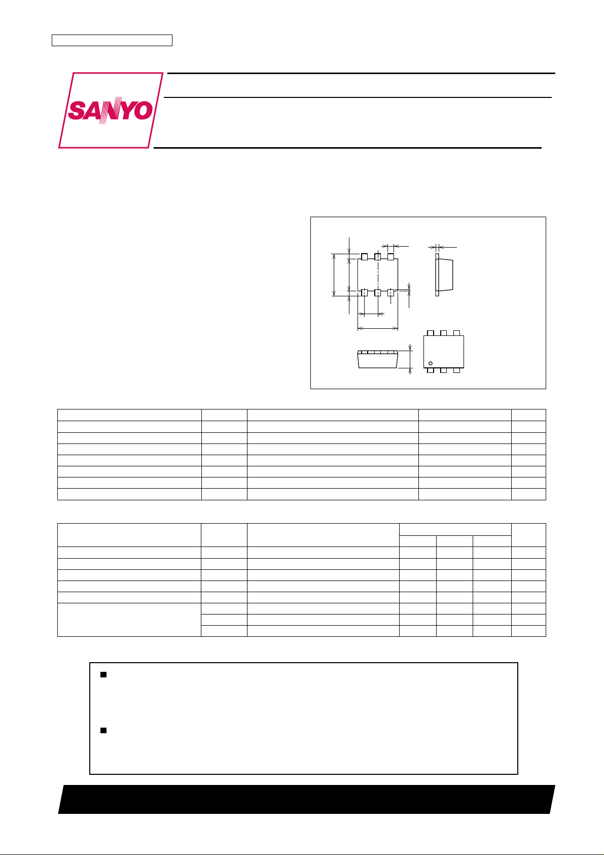
Package Dimensions
unit : mm
2173A
[MCH6608]
0.3
546
1
0.07
2.0
2.1
0.250.25
1.6
32
0.65
0.15
654
1 : Source1
2 : Gate1
3 : Drain2
4 : Source2
5 : Gate2
6 : Drain1
SANYO : MCPH6
Specifications
0.85
123
Absolute Maximum Ratings at T a=25°C
Parameter Symbol Conditions Ratings Unit
Drain-to-Source Voltage V
Gate-to-Source Voltage V
Drain Current (DC) I
Drain Current (Pulse) I
Allowable Power Dissipation P
Channel T emperature T ch 150 °C
Storage T emperature Tstg --55 to +150 °C
DSS
GSS
D
DP
D
PW≤10µs, duty cycle≤1% 2.6 A
Mounted on a ceramic board (900mm2✕0.8mm)1unit
30 V
±10 V
0.65 A
0.8 W
Electrical Characteristics at T a=25°C
Parameter Symbol Conditions
Drain-to-Source Breakdown Voltage V
Zero-Gate Voltage Drain Current I
Gate-to-Source Leakage Current I
Cutoff Voltage VGS(off) VDS=10V , ID=100µA 0.4 1.3 V
Forward Transfer Admittance
Static Drain-to-Source On-State Resistance
(BR)DSSID
DSS
GSS
yfs
RDS(on)1 ID=150mA, VGS=4V 0.9 1.2 Ω
RDS(on)2 ID=80mA, VGS=2.5V 1.2 1.7 Ω
RDS(on)3 ID=10mA, VGS=1.5V 2.6 5.2 Ω
=1mA, VGS=0 30 V
VDS=30V , VGS=0 10 µA
VGS=±8V, VDS=0 ±10 µA
VDS=10V , ID=150mA 400 560 mS
Marking : FH Continued on next page.
Any and all SANYO products described or contained herein do not have specifications that can handle
applications that require extremely high levels of reliability, such as life-support systems, aircraft's
control systems, or other applications whose failure can be reasonably expected to result in serious
physical and/or material damage. Consult with your SANYO representative nearest you before using
any SANYO products described or contained herein in such applications.
SANYO assumes no responsibility for equipment failures that result from using products at values that
exceed, even momentarily, rated values (such as maximum ratings, operating condition ranges, or other
parameters) listed in products specifications of any and all SANYO products described or contained
herein.
Ratings
min typ max
Unit
SANYO Electric Co.,Ltd. Semiconductor Company
TOKYO OFFICE Tokyo Bldg., 1-10, 1 Chome, Ueno, Taito-ku, TOKYO, 110-8534 JAPAN
82201 TS IM TA-2463
No.7040-1/4
Page 2
MCH6608
Continued from preceding page.
Parameter Symbol Conditions
Input Capacitance Ciss VDS=10V , f=1MHz 30 pF
Output Capacitance Coss VDS=10V , f=1MHz 15 pF
Reverse Transfer Capacitance Crss VDS=10V , f=1MHz 10 pF
Turn-ON Delay Time td(on) See specified Test Circuit. 32 ns
Rise Time t
Turn-OFF Delay Time td(off) See specified Test Circuit. 250 ns
Fall Time t
Total Gate Charge Qg VDS=10V, VGS=10V, ID=300mA 2.34 nC
Gate-to-Source Charge Qgs VDS=10V, VGS=10V, ID=300mA 0.38 nC
Gate-to-Drain “Miller” Charge Qgd VDS=10V, VGS=10V, ID=300mA 0.45 nC
Diode Forward Voltage V
SD
See specified Test Circuit. 110 ns
r
See specified Test Circuit. 160 ns
f
IS=300mA, VGS=0 0.8 1.2 V
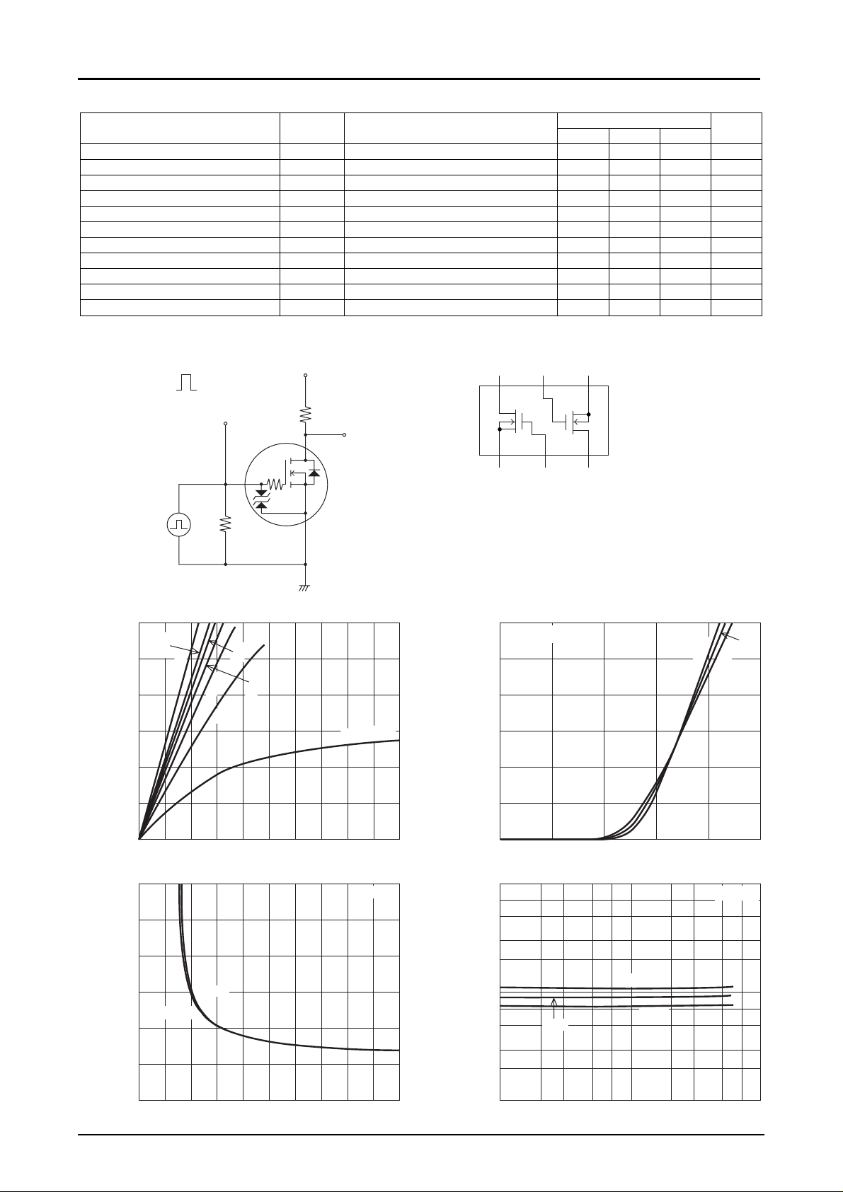
Switching Time Test Circuit Electrical Connection
V
IN
4V
0V
PW=10µs
D.C.≤1%
V
IN
G
VDD=15V
ID=150mA
RL=100Ω
D
V
D1 G2 S2
OUT
S1 D2G1
Ratings
min typ max
Unit
P.G
0.30
0.25
4.0V
6.0V
-- A
0.20
D
0.15
0.10
Drain Current, I
0.05
000.1
3.0
2.5
2.0
(on) -- Ω
0.2
DS
1.5
ID=80mA
1.0
0.5
Static Drain-to-Source
On-State Resistance, R
001
50Ω
I
-- V
D
DS
3.5V
2.5V
3.0V
2.0V
0.3
0.4
0.5 0.6 0.7 0.8 0.9 1.0
Drain-to-Source V oltage, V
RDS(on) -- V
150mA
2
3
4
5
Gate-to-Source V oltage, V
6
MCH6608
S
=1.5V
V
GS
-- V
DS
IT00224 IT00225
GS
Ta=25°C
78910
GS
IT00226 IT00227
-- V
0.6
VDS=10V
0.5
-- A
0.4
D
0.3
0.2
Drain Current, I
0.1
0
0
10
7
5
3
(on) -- Ω
2
0.5 1.0 1.5 2.0
DS
1.0
7
5
3
2
Static Drain-to-Source
On-State Resistance, R
0.1
0.01
25°C
23 57 23 57
I
-- V
D
GS
Gate-to-Source V oltage, V
RDS(on) -- I
Ta=75°C
--25°C
Drain Current, I
0.1
D
GS
D
-- A
Ta= --25°C
-- V
VGS=4V
No.7040-2/4
25°C
75°C
2.5
1.0
Page 3
MCH6608
10
7
5
3
(on) -- Ω
2
DS
1.0
7
5
3
2
Static Drain-to-Source
On-State Resistance, R
0.1
0.01
3.0
2.5
2.0
(on) -- Ω
23 57 23 57
DS
1.5
1.0
0.5
Static Drain-to-Source
On-State Resistance, R
--600--40
1.0
7
5
3
-- A
2
F
0.1
7
5
3
Forward Current, I
2
--20
RDS(on) -- I
D
Ta=75°C
0.1
--25°C
D
-- A
25°C
Drain Current, I
RDS(on) -- Ta
=2.5V
I
F
40
-- V
Ta=75°C
GS
=4.0V
GS
60
80 100 120 160140
SD
25°C
--25°C
=80mA, V
I
D
=150mA, V
I
D
0
20
Ambient Temperature, Ta -- °C
VGS=2.5V
IT00228
IT00230
VGS=0
1.0
10
7
5
(on) -- Ω
RDS(on) -- I
DS
3
2
Static Drain-to-Source
On-State Resistance, R
1.0
0.001 0.01
Ta=75°C
25°C
23 57 23
Drain Current, I
y
Ta= --25°C
25°C
Forward Transfer Admittance, yfs -- S
1.0
0.1
10
7
5
3
2
7
5
3
2
0.01
23 57 23 57
Drain Current, I
SW Time -- I
Switching Time, SW Time -- ns
1000
7
5
3
2
100
7
5
3
2
--25°C
fs -- I
0.1
t
d
t
f
t
r
td(on)
D
D
(off)
-- A
D
75°C
-- A
D
VGS=1.5V
IT00229
VDS=10V
1.0
IT00231
D
VDD=15V
VGS=4V
Ciss, Coss, Crss -- pF
0.01
100
1.0
0
Diode Forward V oltage, V
Ciss, Coss, Crss -- V
7
5
3
2
0.6 0.8 1.0 1.20.2 0.4
-- V
SD
DS
Ciss
1.4
IT00232 IT00233
f=1MHz
Coss
10
7
5
3
2
0
5
10 15
Drain-to-Source V oltage, V
Crss
20 3025
-- V
DS
IT00234 IT00235
10
0.01 0.1
Drain Current, I
10
9
8
-- V
7
GS
6
5
4
3
2
Gate-to-Source V oltage, V
1
0
0
VDS=10V
ID=300mA
0.5
VGS -- Qg
1.0
Total Gate Charge, Qg -- nC
D
1.5
23 523 57
-- A
2.0 2.5
No.7040-3/4
Page 4
5
I
=2.6A
DP
3
2
1.0
I
=0.65A
D
7
-- A
5
D
3
2
0.1
Operation in this
7
Drain Current, I
area is limited by RDS(on).
5
3
Ta=25°C
2
Single pulse
Mounted on a ceramic board(900mm2✕0.8mm)1unit
0.01
23 57 23 57
0.1
A S O
DC operation
1.0 10
Drain-to-Source V oltage, V
100ms
DS
10ms
-- V
<10µs
1ms
23 5
IT03638
MCH6608
1.0
-- W
0.8
D
0.6
0.4
0.2
Allowable Power Dissipation, P
0020 40 60
P
-- Ta
D
Mounted on a ceramic board(900mm
2
✕0.8mm)1unit
80 100 120
Ambient Temperature, Ta -- °C
140 160
IT03637
Note on usage : Since the MCH6608 is designed for high-speed switching applications, please avoid using
this device in the vicinity of highly charged objects.
Specifications of any and all SANYO products described or contained herein stipulate the performance,
characteristics, and functions of the described products in the independent state, and are not guarantees
of the performance, characteristics, and functions of the described products as mounted in the customer's
products or equipment. To verify symptoms and states that cannot be evaluated in an independent device,
the customer should always evaluate and test devices mounted in the customer's products or equipment.
SANYO Electric Co., Ltd. strives to supply high-quality high-reliability products. However, any and all
semiconductor products fail with some probability. It is possible that these probabilistic failures could
give rise to accidents or events that could endanger human lives, that could give rise to smoke or fire,
or that could cause damage to other property. When designing equipment, adopt safety measures so
that these kinds of accidents or events cannot occur. Such measures include but are not limited to protective
circuits and error prevention circuits for safe design, redundant design, and structural design.
In the event that any or all SANYO products(including technical data,services) described or
contained herein are controlled under any of applicable local export control laws and regulations,
such products must not be exported without obtaining the export license from the authorities
concerned in accordance with the above law.
No part of this publication may be reproduced or transmitted in any form or by any means, electronic or
mechanical, including photocopying and recording, or any information storage or retrieval system,
or otherwise, without the prior written permission of SANYO Electric Co. , Ltd.
Any and all information described or contained herein are subject to change without notice due to
product/technology improvement, etc. When designing equipment, refer to the "Delivery Specification"
for the SANYO product that you intend to use.
Information (including circuit diagrams and circuit parameters) herein is for example only ; it is not
guaranteed for volume production. SANYO believes information herein is accurate and reliable, but
no guarantees are made or implied regarding its use or any infringements of intellectual property rights
or other rights of third parties.
This catalog provides information as of August, 2001. Specifications and information herein are subject
to change without notice.
No.7040-4/4
PS
 Loading...