

Page 1
Any and all SANYO products described or contained herein do not have specifications that can handle
applications that require extremely high levels of reliability, such as life-support systems, aircraft’s
control systems, or other applications whose failure can be reasonably expected to result in serious
physical and/or material damage. Consult with your SANYO representative nearest you before using
any SANYO products described or contained herein in such applications.
SANYO assumes no responsibility for equipment failures that result from using products at values that
exceed, even momentarily, rated values (such as maximum ratings, operating condition ranges,or other
parameters) listed in products specifications of any and all SANYO products described or contained
herein.
PNP/NPN Epitaxial Planar Silicon Transistors
DC/DC Converter Applications
Ordering number:ENN6611
MCH6103/MCH6203
SANYO Electric Co.,Ltd. Semiconductor Company
TOKYO OFFICE Tokyo Bldg., 1-10, 1 Chome, Ueno, Taito-ku, TOKYO, 110-8534 JAPAN
Applications
· Relay drivers, lamp drivers, motor drivers and
strobes.
Features
· Adoption of MBIT processes.
· Large current capacitance.
· Low collector-to-emitter saturation voltage.
· High-speed switching.
· Ultrasmall package facilitates miniaturization in end
products (mounting height : 0.85mm).
· High allowable power dissipation.
Specifications
( ) : MCH6103
Absolute Maximum Ratings at Ta = 25˚C
retemaraPlobmySsnoitidnoCsgnitaRtinU
egatloVesaB-ot-rotcelloCV
egatloVrettimE-ot-rotcelloC
egatloVesaB-ot-rettimEV
tnerruCrotcelloCI
)esluP(tnerruCrotcelloCI
tnerruCesaBI
noitapissiDrotcelloCP
erutarepmeTnoitcnuJjT 051
erutarepmeTegarotSgtsT 051+ot55–
OBC
V
SEC
V
OEC
OBE
C
PC
B
Mounted on a ceramic board (600mm2×0.8mm)
C
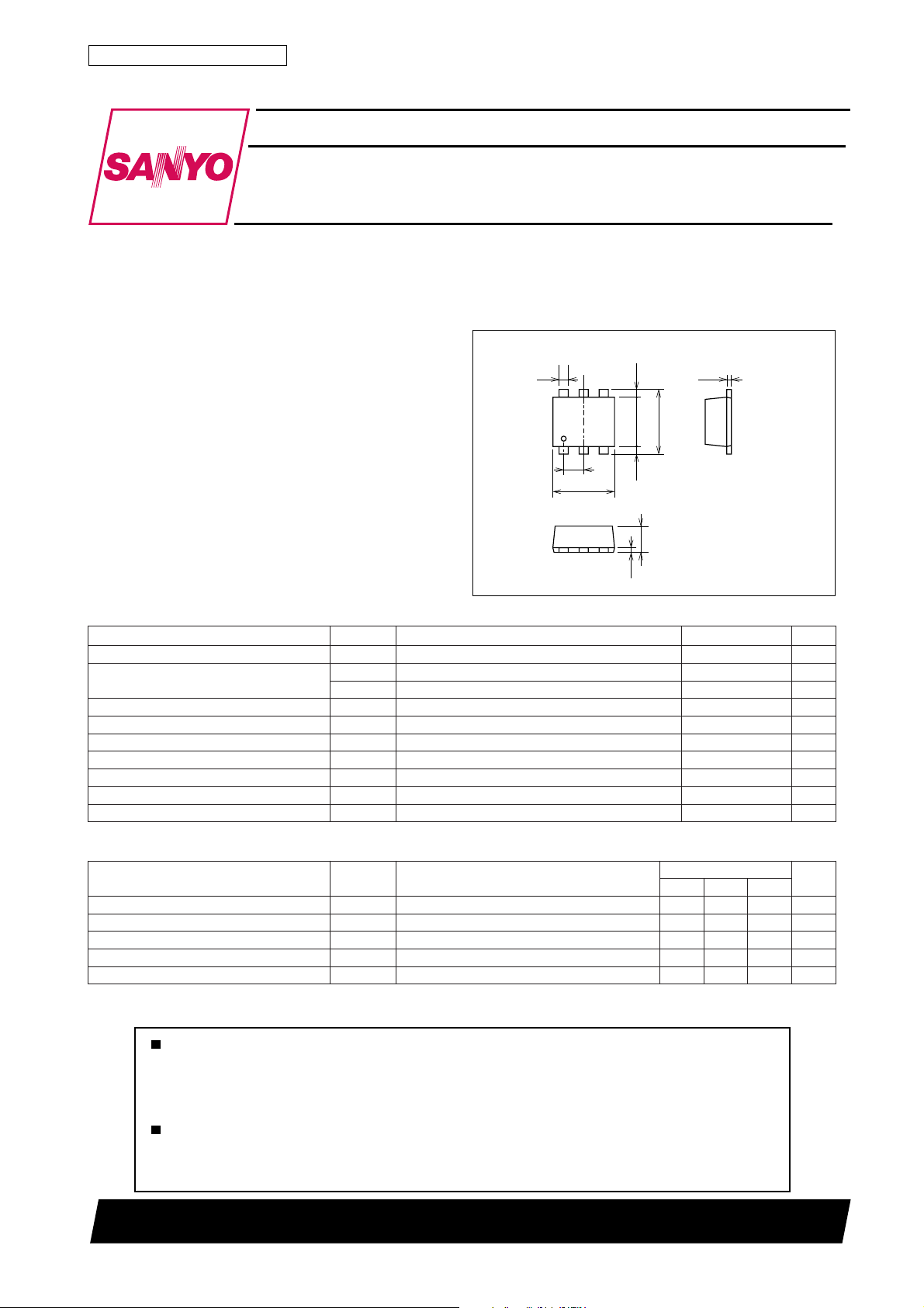
Package Dimensions
unit:mm
2177
[MCH6103/MCH6203]
0.3
5
64
2
13
0.65
2.0
0.15
0.250.25
1.6
2.1
0.85
0.15
1 : Collector
2 : Collector
3 : Base
4 : Emitter
5 : Collector
6 : Collector
SANYO : MCPH6
08)05–(V
08)05–(V
05)–(V
5)–(V
0.1)–(A
3)–(A
002Am
0.1W
˚C
˚C
Electrical Characteristics at Ta = 25˚C
retemaraPlobmySsnoitidnoC
tnerruCffotuCrotcelloCI
tnerruCffotuCrettimEI
niaGtnerruCCD
tcudorPhtdiwdnaB-niaGf
ecnaticapaCtuptuOboCV
h
V
OBC
OBE
EF
T
BC
V
BE
V
EC
V
EC
BC
I,V04)–(=
0=1.0)–(Aµ
E
I,V4)–(=
0=1.0)–(Aµ
C
I,V2)–(=
C
I,V01)–(=
C
Am001)–(=
Am003)–(=024zHM
zHM1=f,V01)–(=
nimpytxam
Marking : MCH6103 : AC, MCH6203 : CC Continued on next page.
N2000TS (KOTO) TA-2974 No.6611–1/5
sgnitaR
002065
6)9(Fp
tinU
Page 2
MCH6103/MCH6203
Continued from preceding page.
retemaraPlobmySsnoitidnoC
I
egatloVnoitarutaSrettimE-ot-rotcelloCV
egatloVnoitarutaSrettimE-ot-esaBV
egatloVnwodkaerBesaB-ot-rotcelloCV
egatloVnwodkaerBrettimE-ot-rotcelloC
egatloVnwodkaerBesaB-ot-rettimEV
emiTNO-nruTt
emiTegarotSt
emiTllaFt
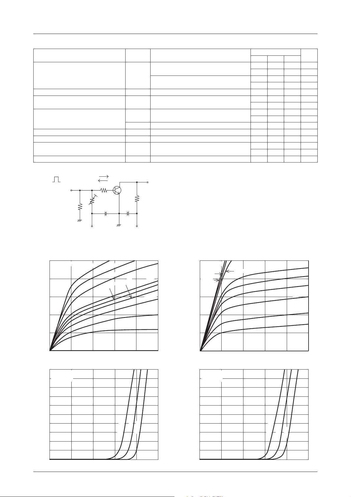
Switching Time Test Circuit
PW=20µs
D.C.≤1%
I
B1
I
B2
EC
EB
V
V
)tas(
)tas(I
OBC)RB(
SEC)RB(
OEC)RB(
OBE)RB(
no
gts
f
OUTPUT
C
I
C
C
I
C
I
C
I
C
I
E
I,Am005)–(=
B
I,Am003)–(=
B
I,Am005)–(=
B
I,Aµ01)–(=
E
R,Aµ001)–(=
R,Am1)–(=
EB
I,Aµ01)–(=
C
Am01)–(=
Am6)–(=
Am01)–(=18.0)–(2.1)–(V
0=
0=
EB
=∞ 05)–(V
0=5)–(V
.tiucrictsetdeificepseeS
.tiucrictsetdeificepseeS
.tiucrictsetdeificepseeS
sgnitaR
nimpytxam
)082–()034–(Vm
031091Vm
)541–()022–(Vm
09531Vm
)05–(V
08V
)05–(V
08V
83)63(sn
)371(sn
233sn
04)82(sn
tinU
INPUT
50Ω
IC=20IB1= --20IB2=500mA
For PNP, the polarity is reversed.
--1.0
MCH6103
--0.8
–A
C
--0.6
--0.4
Collector Current, I
--0.2
0
0 --200 --400 --600 --800 --1000
Collector-to-Emitter Voltage, VCE–mV
--1.0
MCH6103
--0.9
VCE= --2V
--0.8
–A
--0.7
C
--0.6
--0.5
--0.4
--0.3
Collector Current, I
--0.2
--0.1
0
0 --0.2 --0.4 --0.6 --0.8 --1.0
V
R
I
--40mA
I
C
C
R
B
+
100µF 470µF
-- V
CE
--30mA
--20mA
--6mA
--8mA
-- V
BE
°C
Ta=75
+
VCC=25VVBE= --5V
°C
25
Base-to-Emitter Voltage, VBE–V
R
L
50Ω
--10mA
--4mA
--2mA
--1mA
IT01890
°C
--25
IT01892
IB=0
1.0
MCH6203
30mA
0.8
40mA
C
20mA
CE
I
-- V
–A
C
0.6
0.4
Collector Current, I
0.2
0
0 200 400 600 800 1000
Collector-to-Emitter Voltage, VCE–mV
I
-- V
1.0
MCH6203
0.9
VCE=2V
0.8
0.7
–A
C
0.6
0.5
0.4
0.3
Collector Current, I
0.2
0.1
0
0 0.2 0.4 0.6 0.8 1.0
C
BE
°C
Ta=75
25
°C
°C
--25
Base-to-Emitter Voltage, VBE–V
10mA
8mA
6mA
4mA
2mA
1mA
IB=0
IT01891
IT01893
No.6611–2/5
Page 3
1000
FE
MCH6103/MCH6203
h
h
-- I
FE
7
5
3
2
Ta=75°C
--25
°C
25°C
C
MCH6103
VCE= --2V
1000
FE
7
5
3
2
Ta=75
FE
°C
--25°C
-- I
25°C
C
MCH6203
VCE=2V
100
7
5
DC Current Gain, h
3
2
10
--0.01
--1000
7
5
3
(sat) – mV
2
CE
--100
7
5
3
2
Collector-to-Emitter
Saturation Voltage, V
--10
--0.01 --0.1
--10000
7
5
3
2
--1000
(sat) – mV
7
5
CE
3
2
--100
7
5
3
Collector-to-Emitter
Saturation Voltage, V
2
--10
--0.01 --0.1
--10000
7
5
3
2
(sat) – mV
BE
--1000
7
5
3
2
Base-to-Emitter
Saturation Voltage, V
--100
--0.01 --0.1
23 57 23 57
23 57 23 57
23 57 23 57
325
Collector Current, IC–A
73257
--0.1
VCE(sat) -- I
°C
Ta=75
--25
°C
C
25°C
Collector Current, IC–A
VCE(sat) -- I
Ta=75
--25
°C
°C
C
25°C
Collector Current, IC–A
VBE(sat) -- I
°C
Ta= --25
°C
75
C
25°C
Collector Current, IC–A
IT01894
MCH6103
IC / IB=20
IT01896
MCH6103
IC / IB=50
IT01898
MCH6103
IC / IB=50
IT01900
--1.0
--1.0
--1.0
--1.0
100
7
5
DC Current Gain, h
3
2
10
0.01
1000
7
5
3
(sat) – mV
2
CE
100
7
5
3
2
Collector-to-Emitter
Saturation Voltage, V
10
0.01 0.1
10000
7
5
3
2
1000
(sat) – mV
7
CE
5
3
2
100
7
5
3
Collector-to-Emitter
Saturation Voltage, V
2
10
0.01 0.1
10000
7
5
3
2
(sat) – mV
BE
1000
7
5
3
2
Base-to-Emitter
Saturation Voltage, V
100
0.01 0.1
23 57 23 57
23 57 23 57
23 57 23 57
325
73257
Collector Current, IC–A
0.1
VCE(sat) -- I
°C
Ta=75
°C
--25
Collector Current, IC–A
VCE(sat) -- I
°C
Ta=75
°C
--25
Collector Current, IC–A
VBE(sat) -- I
°C
Ta= --25
75°C
25°C
Collector Current, IC–A
C
C
C
MCH6203
IC / IB=20
25°C
MCH6203
IC / IB=50
25°C
MCH6203
IC / IB=50
No.6611–3/5
IT01895
IT01897
IT01899
IT01901
1.0
1.0
1.0
1.0
Page 4
MCH6103/MCH6203
5
3
2
100
7
5
3
2
10
7
Output Capacitance, Cob – pF
5
3
2
23 57 23 5 23 57
--0.1 --10
1000
7
– MHz
5
T
3
Collector-to-Base Voltage, VCB–V
Cob -- V
--1.0
f
T
-- I
CB
C
MCH6103
f=1MHz
IT01902
MCH6103
VCE= --10V
5
3
2
100
7
5
3
2
10
7
Output Capacitance, Cob – pF
5
3
2
2 3 57 2 3 57
0.1 1.0
1000
7
– MHz
5
Collector-to-Base Voltage, VCB–V
T
3
Cob -- V
f
-- I
T
CB
C
MCH6203
f=1MHz
10
MCH6203
VCE=10V
23 5
IT01903
2
Gain-Bandwidth Product, f
100
--0.01
5
3
2
1.0
–A
7
C
5
3
2
0.1
7
5
Collector Current, I
3
2
0.01
25732573
Collector Current, IC–A
ICP=3A
IC=1A
Ta=25°C
Single pulse
For PNP, minus sign is omitted.
Mounted on a ceramic board(600mm
2537102537
Collector-to-Emitter Voltage, VCE–V
1.00.1
2
Gain-Bandwidth Product, f
--0.1 --1.0 0.01 0.1
IT01904
A S O
MCH6103 / MCH6203
500µs
2
×0.8mm)
100µs
1ms
2537
100
IT01906
10ms
100ms
DC operation
100
1.4
1.2
–W
1.0
C
0.8
0.6
0.4
Collector Dissipation, P
0.2
0
25732573
Collector Current, IC–A
P
Mounted on a ceramic board (600mm
2006040 80 100 140120 160
Ambient Temperature, Ta – °C
-- Ta
C
MCH6103 / MCH6203
2
×0.8mm)
1.0
IT01905
IT01907
No.6611–4/5
Page 5
MCH6103/MCH6203
Specifications of any and all SANYO products described or contained herein stipulate the performance,
characteristics, and functions of the described products in the independent state, and are not guarantees
of the performance, characteristics, and functions of the described products as mounted in the customer's
products or equipment. To verify symptoms and states that cannot be evaluated in an independent device,
the customer should always evaluate and test devices mounted in the customer's products or equipment.
SANYO Electric Co., Ltd. strives to supply high-quality high-reliability products. However, any and all
semiconductor products fail with some probability. It is possible that these probabilistic failures could
give rise to accidents or events that could endanger human lives, that could give rise to smoke or fire,
or that could cause damage to other property. When designing equipment, adopt safety measures so
that these kinds of accidents or events cannot occur. Such measures include but are not limited to protective
circuits and error prevention circuits for safe design, redundant design, and structural design.
In the event that any or all SANYO products(including technical data,services) described or
contained herein are controlled under any of applicable local export control laws and regulations,
such products must not be exported without obtaining the export license from the authorities
concerned in accordance with the above law.
No part of this publication may be reproduced or transmitted in any form or by any means, electronic or
mechanical, including photocopying and recording, or any information storage or retrieval system,
or otherwise, without the prior written permission of SANYO Electric Co. , Ltd.
Any and all information described or contained herein are subject to change without notice due to
product/technology improvement, etc. When designing equipment, refer to the "Delivery Specification"
for the SANYO product that you intend to use.
Information (including circuit diagrams and circuit parameters) herein is for example only ; it is not
guaranteed for volume production. SANYO believes information herein is accurate and reliable, but
no guarantees are made or implied regarding its use or any infringements of intellectual property rights
or other rights of third parties.
This catalog provides information as of November, 2000. Specifications and information herein are subject
to change without notice.
PS No.6611–5/5
 Loading...