

Page 1

DATA SHEET
HYBRID INTEGRATED CIRCUIT
MC-9400A
320 (240)-BIT AC- PDP DRIVER MODULE
DESCRIPTION
The MC-9400A is a PDP driver module that incorporates five 64-bit high breakdown voltage output (150 V, 40 mA)
CMOS driver ICs. It supports 320 outputs in the case of 4-bit parallel input, and 240 outputs in the case of 3-bit parallel
input.
The integrated structure of the MC-9400A, which combines a COB with an aluminum heat sink and an output flexible
printed circuit (FPC) board, enables the easy implementation of heat dissipation measures and high-density mounting.
FEATURES
• Incorporates five µPD16337s with four 16-bit bi-directional shift registers
• Low thermal resistance realized by chip-on-metal structure
• Provided with connector and capacitor for easy mounting on a panel
• Supports output electrode with a narrow pitch through use of a flexible printed circuit board
• Polarity of all driver outputs can be inverted through use of /PC pins
• Supports custom modules
Remark
/XXX indicates active low.
ORDERING INFORMATI O N
Part Number Package
MC-9400A COB
The information in this document is subject to change without notice.
Document No. S13787EJ2V0DS00 (2nd edition)
Data Published October 1998 NS CP(K)
Printed in Japan
The mark
★★★★
shows major revised points.
© NEC Corporation 1998
Page 2
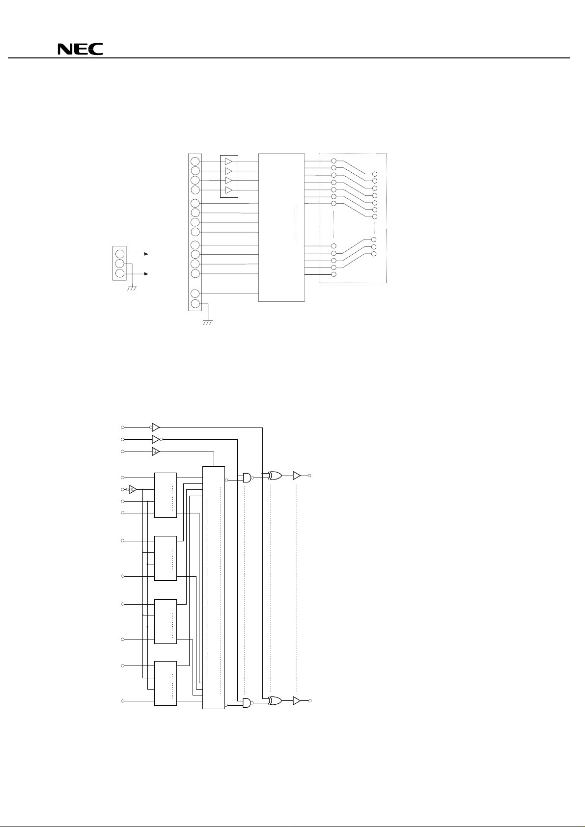
BLOCK DIAGRAM (1/ 5 CIRCUIT)
CN3
CN1,2
V
DD1
(Logic power supply)
VDD2
(Driver power supply)
74AC244
µ
PD16337
/PC O1
BLK
LE
R,/L
1
A
A2
A3
A4
B1
B2
B3
B4
/CLK
O2
O3
O4
O5
O6
O7
O60
O61
O62
O63
O64
MC-9400A
Remark
PD16337s incorporated : 240 outputs at 3 ch and 320 outputs at 4 ch.
Five
µ
See the following block diagram for the
PD16337 BLOCK DIAGRAM
µµµµ
/PC
BLK
LE
SR1
A
1
/CLK CLK
R,/L R,/L
B
1
A
2
B
2
A
3
B
3
A
B
A
CLK
R,/L
B
A
CLK
R,/L
B
S
1
1
5
S
S
61
1
SR2
S
2
2
6
S
S
62
2
SR3
S
3
3
7
S
S
63
3
PD16337.
µ
LE
/L
1
S
1
S
2
S
3
S
4
Note
O
1
2
A
4
B
4
SRn : 16-bit shift register
Note
SR4
S
A
4
4
8
S
CLK
R,/L
B
S
64
4
S
61
S
62
S
63
S
64
/L
64
S
High breakdown voltage CMOS driver 150V, ±40 mA(MAX.).
64
Page 3
★
PIN CONFIGURATION ( Top Vi ew)
CN3
B
54
B
53
B
52
B
51
A
51
A
52
A
53
A
54
B
44
B
43
B
42
B
41
A
41
A
42
A
43
A
44
GND 34
/CLK 33
GND 32
LE 31
GND 30
R,/L 29
GND 28
/PC 27
GND 26
BLK 25
B
34
B
33
B
32
B
31
A
31
A
32
A
33
A
34
B
24
B
23
B
22
B
21
A
21
A
22
A
23
A
24
B
14
B
13
B
12
B
11
A
11
A
12
A
13
A
14
50
49
48
47
46
45
44
43
42
41
40
39
38
37
36
35
24
23
22
21
20
19
18
17
16
15
14
13
12
11
10
9
8
7
6
5
4
3
2
1
CN2
V
DD2
1
GND 2
V
DD1
3
CN1
V
DD2
1
GND 2
V
DD1
3
EPC
O
O
O
O
O
O
O
O
O
O
MC-9400A
320
257
256
194
193
129
128
65
64
1
Caution To prevent latch-up breakage, be sure to turn the power on in the order of V
signal, and V
DD2
, and turn the power off in the reverse order. Keep this order also during
a transition period.
DD1
, logic
3
Page 4
PIN FUNCTIONS
Pin Symbol Pin Name Pin No. I/O Description
MC-9400A
/PC Polarity inverted
27 CN3 /PC = L : Polarity of all outputs inverted
input
BLK Blanking input 25 CN3 BLK = H : All outputs = H or L
LE Latch enable input 31 CN3 Automatically latches by a high level input at the rising edge of the
clock
A11 to A14,
21
to A24,
A
31
to A34,
A
41
to A44,
A
51
to A
A
B11 to B14,
21
to B24,
B
31
to B34,
B
41
to B44,
B
51
to B
B
RIGHT data input 1 to 4
54
LEFT data input 5 to 8
54
9 to 12
17 to 20
35 to 38
46
13 to 16
21 to 24
39 to 42
47 to 50
CN3
CN3
When R,/L = H
11
to A14, A21 to A24, A31 to A34, A41 to A44, A51 to A
A
11
to B14, B21 to B24, B31 to B34, B41 to B44, B51 to B
B
When R,/L = L
11
to A14, A21 to A24, A31 to A34, A41 to A44, A51 to A
A
11
to B14, B21 to B24, B31 to B34, B41 to B44, B51 to B
B
54
: Input
54
: Output
54
: Output
54
: Input
/CLK Clock i nput 33 CN3 Executes a shi ft at the rising edge
R,/L Shi f t control input 29 CN3
Right shift mode by H
→
1
1
1
SR
: A
61
... S
S
→
1
(SR2, SR3, and SR4 also same direction)
B
Left shift mode by L
→
1
1
: B
SR
S
61
... S
→
1
1
(SR2, SR3, and SR4 also same direction)
A
320
O1 to O
High breakdown
voltage output
DD1
V
Logic block power
supply
DD2
V
Driver block power
supply
GND Ground
4
1 to 320 FPC 150 V, 40mA (MA X.)
1 CN1
5 V ± 10 %
CN2
3 CN1
30 V to 130 V
CN2
2 CN1
Connected to system ground
CN2
26,28,
CN3
30,32,
34
Page 5
TRUTH TABLE
1. Shift register block
Input Output
R,/L /CLK A B
↓
↓
Input
Output
57
, S58, S59, and S60 are shifted to S61, S62, S63, and S64, and output from B1, B2, B3,
Note2
Notes 1.
2.
H
HX
L
L X Output
On a clock rise, the data S
and B4, respectively.
On a clock fall, the data S5, S6, S7, and S8 are shifted to S1, S2, S3, and S4, and output from A1, A2, A3, and A4,
respectively.
Output
Output Retain
Input
Note1
Execution of right s hi f t
Execution of left s hi ft
Retain
MC-9400A
Shift register
Remark
X= H or L, H= High level, L= Low level
2. Latch block
LE /CLK Output state of latc h bl ock (/Ln)
Remark
H
↓
↓
L X Retains the latch data
X= H or L, H= High level, L= Low level
Latches the data of Sn and retai ns the output data
Retains the latch data
3. Driver block
/Ln BLK /PC Driver output state
X H H H (all driver outputs : H)
X H L L (all driver outputs : L)
X L H Outputs latch data (/Ln)
X L L Outputs latch data (/Ln) with polarity inverted
Remark
X= H or L, H= High level, L= Low level
5
Page 6

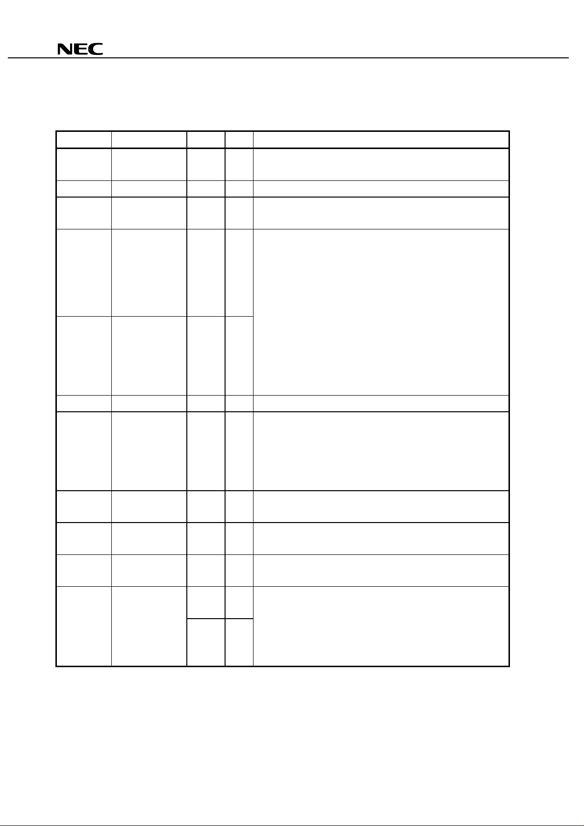
ELECTRICAL CHARACTERISTICS
Absolute maximum ratings (TA = +25
Parameter Symbol Ratings Unit
Logic block supply v ol t age V
°°°°
C, V
DD1
SS1
= V
SS2
= 0 V)
MC-9400A
−
0.5 to + 7.0 V
Driver block supply v ol t age V
Logic block input volt age V
Driver block output current I
Module allowable power dissipation P d
Junction temperature Tj
Operating ambient temperature T
Storage temperature T
The value when mounting this driver module on the aluminum frame by screw.
Note
DD2
1
O2
MAX.
MAX.
A
stg
−
0.5 to + 150 V
−
0.5 to V
DD1
+ 0.5 V
40 mA
Note
6
125
−
10 to + 70
−
40 to + 85
W
°
C
°
C
°
C
Caution If the absolute maximum rating of even one of the above parameters is exceeded even momentarily,
the quality of the product may be degraded. Absolute maximum ratings, therefore,specify the values
exceeding which the product may be physically damaged. Be sure to use the product within the
range of the absolute maximum ratings.
−−−−
Recommended operating range (T
A
=
10 to + 70
Parameter Symbol MIN. TYP. MAX. Unit
Logic block supply v ol t age V
Driver block supply v ol t age V
Input voltage high V
Input voltage low V
Driver output current
°°°°
C, V
DD1
DD2
OH2
I
OL2
I
SS1
SS2
= V
= 0 V)
4.5 5.0 5.5 V
30 130 V
IH
IL
DD1
0.7 V
0 0.2 V
−
30 mA
DD1
V
DD1
V
V
+30 mA
6
Page 7

MC-9400A
Electrical specifications
(TA = +25
Parameter Symbol Conditions MIN. TYP. MAX. Unit
Output voltage high V
Output voltage high V
Output voltage low V
Output voltage low V
Input leakage current (H1) PU I
Input leakage current (H2) PC I
Input leakage current (L2) PC I
Input voltage high V
Input voltage low V
Power supply current 1(Logic) I
Power supply current 1(Logic) I
Power supply current 2
(Driver)
Power supply current 2
(Driver)
Power supply current 2
(Driver)
DD1
DD1
OH21
OH22
OL21
OL22
LIH1
LIH2
LIL2
DD2
I
DD2
I
DD2
I
°°°°
SS1
= V
DD2
= 130 V,I
DD2
= 130 V,I
DD2
= 130 V,I
DD2
= 130 V,I
DD1
= 7.0 V,V
DD1
= 7.0 V,V
DD1
= 7.0 V,V
DD1
= 5.0 V,V
DD1
= 5.0 V,V
DD1
= 7.0 V
DD1
= 5.0 V
DD2
=135 V
SS2
= 0 V)
OH
= −10 mA 123 V
OH
= −30 mA 110 V
OH
= 10 mA 5.0 V
OH
= 30 mA 15.0 V
DD2
= 30 V
DD2
= 30 V
DD2
= 30 V
DD2
= 30 V 3.5 V
DD2
= 30 V 1.0 V
−
4.0 +4.0
−
4.0 +4.0
−
4.0 +4.0
In : High Level 80
Out : ALL Low 500
Out : ALL High 500
Out :HLHLLHLH 500
µ
A
µ
A
µ
A
8mA
µ
A
µ
A
µ
A
µ
A
C, V
V
V
V
V
V
V
V
IH
V
IL
V
a1
V
–1
V
V
Power supply current 2
(Driver)
Switching characteristics
(TA = +25
Parameter Symbol Conditions MIN. TYP. MAX. Unit
Propagation delay time t
Propagation delay time t
Propagation delay time t
Propagation delay time t
Propagation delay time t
Propagation delay time t
Rise time t
Fall time t
Maximum clock f requency f
DD2
I
PLH2
PHL2
PLH3
PHL3
PLH4
PHL4
TLH
THL
MAX.
°°°°
SS1
C, V
DD1
V
DD1
V
DD1
V
BLK→OUT
DD1
V
BLK→OUT
DD1
V
PC→OUT
DD1
V
PC→OUT
DD1
V
DD1
V
DD1
V
SS2
= V
= 5.0 V, V
= 5.0 V, V
= 5.0 V, V
= 5.0 V, V
= 5.0 V, V
= 5.0 V, V
= 5.0 V, V
= 5.0 V, V
= 4.0 V, V
Out :LHLHHLHL 500
= 0 V)
DD2
= 130 V 187.5 ns
DD2
= 130 V 187.5 ns
DD2
= 130 V,
DD2
= 130 V,
DD2
= 130 V,
DD2
= 130 V,
DD2
= 130 V 200.0 ns
DD2
= 130 V 200.0 ns
DD2
= 30 V 25.0 MH
172.5 ns
172.5 ns
160.0 ns
160.0 ns
µ
A
Z
7
Page 8

MC-9400A
Timing requirements
(TA = +25
Parameter Symbol Conditions MIN. TYP. MAX. Unit
Data setup time 1 t
Data setup time 2 t
Data hold time t
Latch enable time 1 t
Latch enable time 2 t
Latch enable time 3 t
Latch enable time 4 t
°°°°
SS1
C, V
= V
SETUP1VDD1
SETUP2VDD1
HOLDVDD1
LE1
V
LE2
V
LE3
V
LE4
V
SS2
= 4.5 V, V
= 4.5 V, V
= 4.5 V, V
DD1
= 4.5 V, V
DD1
= 4.5 V, V
DD1
= 4.5 V, V
DD1
= 4.5 V, V
= 0 V)
DD2
= 30 V 31.2 ns
DD2
= 30 V 12.0 ns
DD2
= 30 V 8.5 ns
DD2
= 30 V 27.5 ns
DD2
= 30 V 17.5 ns
DD2
= 30 V 27.5 ns
DD2
= 30 V 17.5 ns
8
Page 9

Timing chart (Right shift)
/CLK
A
1 (B4)
A
2 (B3)
A
3 (B2)
A
4 (B1)
1 (S64)
S
S
2 (S63)
S
3 (S62)
MC-9400A
S
4 (S61)
S
5 (S60)
S
6 (S59)
S
7 (S58)
S
8 (S57)
O
1 (O64)
O
2 (O63)
O
3 (O62)
O
4 (O61)
LE
BLK
/PC
O
5 (O60)
O
6 (O59)
O
7 (O58)
O
8 (O57)
Remark
() applies when R,/L = L
9
Page 10

Switching characteristics waveform
Propagation delay time
PHL2
, t
PLH2
t
MC-9400A
/CLK2
n
O
O
n
Propagation delay time (BLK
PHL3
, t
PLH3
BLK
t
50 % 50%
t
PHL2
90 %
→→→→
OUT)
50 % 50%
t
PHL3
t
t
PLH3
PLH2
10%
10
O
n
10%
90 %
Page 11

MC-9400A
Propagation delay time (/PC
PHL4
, t
PLH4
t
/PC
n
O
Rise time, Fall time
TLH
, t
THL
On
t
→→→→
OUT)
50% 50%
t
PHL4
90%
t
TLH
90 % 90 %
10%
t
PLH4
10%
t
THL
10%
Maximum clock frequency
MAX.
F
CLK2
1/f
MAX.
50%50%
11
Page 12

Data setup time1, 2, and Data hold time
MC-9400A
t
SETUP1
SETUP2
, t
, t
HOLD
/CLK1
DATA
/CLK2
Latch enable time1, 2, 3, 4
LE1
LE2
, t
LE3, tLE4
, t
t
SETUP2
t
50%
50%
t
HOLD
t
SETUP1
50%
/CLK2
LE
50%
50%
LE1
t
50%
t
LE2
t
LE3
50%
t
LE4
50%
12
Page 13

PACKAGE DRAWING (unit : mm)
COB with radiation board attached + FPC module
101.4
2-10
1.25
10
MC-9400A
15533.0
63
C2
10.95
92.0
MC-9400A
1.5
10.9535.0535.05
C2
7 MAX.
13
Page 14

[MEMO]
MC-9400A
14
Page 15

NOTES FOR CMOS DEVICES
1 PRECAUTION AGAINST ESD FOR SEMICONDUCTORS
Note: Strong electric field, when exposed to a MOS device, can cause destruction
of the gate oxide and ultimately degrade the device operation. Steps must
be taken to stop generation of static electricity as much as possible, and
quickly dissipate it once, when it has occurred. Environmental control must
be adequate. When it is dry, humidifier should be used. It is recommended
to avoid using insulators that easily build static electricity. Semiconductor
devices must be stored and transported in an anti-static container, static
shielding bag or conductive material. All test and measurement tools
including work bench and floor should be grounded. The operator should
be grounded using wrist strap. Semiconductor devices must not be touched
with bare hands. Similar precautions need to be taken for PW boards with
semiconductor devices on it.
MC-9400A
2 HANDLING OF UNUSED INPUT PINS FOR CMOS
Note: No connection for CMOS device inputs can be cause of malfunction. If no
connection is provided to the input pins, it is possible that an internal input
level may be generated due to noise, etc., hence causing malfunction. CMOS
devices behave differently than Bipolar or NMOS devices. Input levels of
CMOS devices must be fixed high or low by using a pull-up or pull-down
DD
circuitry. Each unused pin should be connected to V
resistor, if it is considered to have a possibility of being an output pin. All
handling related to the unused pins must be judged device by device and
related specifications governing the devices.
or GND with a
3 STATUS BEFORE INITIALIZATION OF MOS DEVICES
Note: Power-on does not necessarily define initial status of MOS device. Production
process of MOS does not define the initial operation status of the device.
Immediately after the power source is turned ON, the devices with reset
function have not yet been initialized. Hence, power-on does not guarantee
out-pin levels, I/O settings or contents of registers. Device is not initialized
until the reset signal is received. Reset operation must be executed immediately after power-on for devices having reset function.
15
Page 16

MC-9400A
No part of this document may be copied or reproduced in any form or by any means without the prior written
consent of NEC Corporation. NEC Corporation assumes no responsibility for any errors which may appear in this
document.
NEC Corporation does not assume any liability for infringement of patents, copyrights or other intellectual
property rights of third parties by or arising from use of a device described herein or any other liability arising
from use of such device. No license, either express, implied or otherwise, is granted under any patents,
copyrights or other intellectual property rights of NEC Corporation or others.
While NEC Corporation has been making continuous effort to enhance the reliability of its semiconductor devices,
the possibility of defects cannot be eliminated entirely. To minimize risks of damage or injury to persons or
property arising from a defect in an NEC semiconductor device, customers must incorporate sufficient safety
measures in its design, such as redundancy, fire-containment, and anti-failure features.
NEC devices are classified into the following three quality grades:
"Standard", "Special", and "Specific". The Specific quality grade applies only to devices developed based on
a customer designated "quality assurance program" for a specific application. The recommended applications
of a device depend on its quality grade, as indicated below. Customers must check the quality grade of each
device before using it in a particular application.
Standard: Computers, office equipment, communications equipment, test and measurement equipment,
audio and visual equipment, home electronic appliances, machine tools, personal electronic
equipment and industrial robots
Special: Transportation equipment (automobiles, trains, ships, etc.), traffic control systems, anti-disaster
systems, anti-crime systems, safety equipment and medical equipment (not specifically designed
for life support)
Specific: Aircrafts, aerospace equipment, submersible repeaters, nuclear reactor control systems, life
support systems or medical equipment for life support, etc.
The quality grade of NEC devices is "Standard" unless otherwise specified in NEC’s Data Sheets or Data Books.
If customers intend to use NEC devices for applications other than those specified for Standard quality grade,
they should contact an NEC sales representative in advance.
Anti-radioactive design is not implemented in this product.
M4 96. 5
 Loading...