

Page 1
查询MC92052供应商
MOTOROLA
SEMICONDUCTOR TECHNICAL DATA
Order this Data Sheet by MC92052/D
Product Brief
MC92052
MC92052
FTTC User Framer
The MC92052 is a peripheral device for the user side of an FTTC drop. It is composed of downstream and upstream
TC-sublayer functionality with UTOPIA compliant ATM-layer ports.
MC92052 Features
• Implements the DAVIC short-range baseband asymmetrical physical layer standard
• Supports a bit rate of up to 51.84 Mbit/sec downstream
• Provides TDMA at a bit rate of up to 6.48 Mbit/s upstream, including DAVIC Bit Rates B, C, and D
• Interfaces to an ATM-layer device using a UTOPIA compliant interface
• Performs convolutional deinterleaving of the downstream payload blocks for the full range of interleaving depths
(M = 1-31) using an external 16K x 8 SRAM
• Can optionally use an internal RAM for deinterleaving when the interleaving depth is small (M ≤ 2)
• Performs Reed-Solomon encoding of the upstream frames and decoding of the downstream frames
• Performs HEC-based cell delineation and error correction on the downstream data
• Optionally filters received ATM cells based on GFC/VPI pattern matching
• Includes serial data interfaces to a Physical Medium Dependent (PMD) sublayer device
• Optional serial data link interfaces for upstream and downstream frames
• Includes a power level control interface to the transmitter
• Provides an 8-bit system interface as a generic slave device
• IEEE 1149.1 (JTAG) boundary scan test port
• 3.3 V operation with TTL compatibility on I/O pins
• Extended temperature operation: -40 to 85°C
• Available in 128 Pin Plastic Quad Flat Package
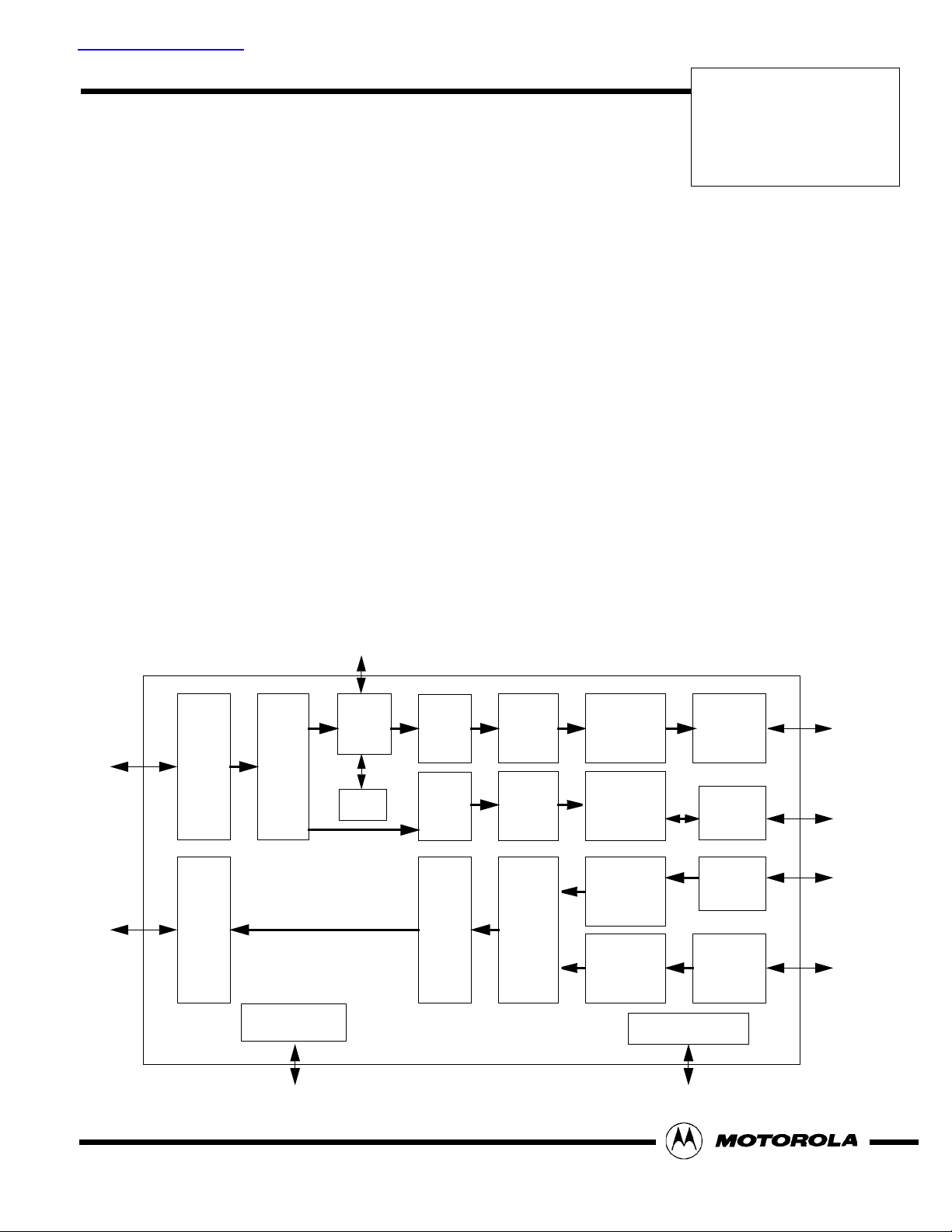
Deinter-
Rx
PMD
I/F
Tx
PMD
I/F
This document contains information on a new product.
Specifications and information herein are subject to change without notice.
MOTOROLA, INC. 1997
Frame
Align-
ment
Microprocessor
Interface
leaver
RAM
Figure 1. MC92052 Block Diagram
Reed-
Solomon
Decoder
Reed-
Solomon
Decoder
Reed-
Solomon
Encoder
Deran-
domizer
Deran-
domizer
Random-
izer
Rx Cell
Functions
Header
Interpretation
Header
Generation
Tx Cell
Functions
JTAG Controller
Rx
UTOPIA
I/F
Data
Link
Extraction
Data
Link
Insertion
Tx
UTOPIA
I/F
Page 2

General Description
The MC92052 implements the TC sublayer of the DAVIC asymmetrical FTTC PHY specification for user devices. The MC92052 key functional blocks are described in
the paragraphs which follow.
Rx PMD Interface
The receive PMD interface receives a clock signal and
a serial data stream. The clock is used both to sample
the data and to clock the operation of the MC92052.
Frame Alignment
When in the “out-of-frame” condition, the frame alignment block searches the serial data (which is LSB first)
for the 16-bit framing pattern and then converts it to 8bit parallel data aligned to the framing pattern. When in
the “in-frame” condition, the serial-to-parallel block verifies the framing pattern and continues to convert it to
parallel data using the current alignment. In each frame,
the two framing bytes are discarded, the next 16 bytes
are provided to the header flow, and the following
(12 * 66) bytes are provided to the payload flow.
Deinterleaver
The deinterleaver block recovers the original data
blocks from the interleaved data that it receives. Transmitting interleaved data allows for better correction of
bursts of errors because the deinterleaver spreads the
incorrect data over many blocks so that the Reed-Solomon decoder can correct the small number of errors
in each block.
The deinterleaver separates the data byte stream into
33 branches. Each of the branches is delayed by a different amount, and then they are recombined into a single data stream. The delay of branch k (0 ≤ k ≤ 32) is
M * (32 - k). M is the Interleaving Depth Parameter recovered from the frame header and ranges from 0 to 31.
M=0 effectively disables the deinterleaver.
The delay of the interleaver/deinterleaver combination
is 1056 * M payload byte periods. The deinterleaver is
implemented using an external SRAM (Motorola
MCM6306 or equivalent). Alternatively, the internal
RAM can be used if the value of M is 1 or 2.
Reed-Solomon Decoders
One Reed-Solomon decoder is used for the header. It
decodes the (16,12) code in order to correct up to 2
bytes or declare the header to be uncorrectable.
The other decoder is used for the payload blocks. It decodes the (66,58) codes in order to correct up to 4 bytes
or declare the block to be uncorrectable, in which case
the data is not touched.
Derandomizers
The received data has been randomized on the network
side for better transmission performance. The derandomizers perform the inverse function to restore the
original data.
The two derandomizers are identical. One is used for
the 12 header bytes per frame, and the other is used for
the 12*58 payload bytes per frame. The derandomizers
are self-synchronizing since they depend only on the
previously received data.
Frame Header Interpretation Block
The header interpretation block extracts the useful information from the received frame header. It provides
information to the transmit flow regarding when to
transmit a cell, etc.
Data Link Extraction
The data link extraction block optionally provides the
data link bytes of the downstream frame headers to a
serial data link controller (e.g., MC68360 QUICC) for
further processing. The received downstream data link
bytes are extracted using a clock pin and a data pin.
Rx Cell Functions
The receive cell functions block recovers 53-octet ATM
cells from the derandomized byte stream using the
HEC-based method described in ITU-T Recommendation I.432.
Once the cell alignment has been recovered, the receive cell functions block checks the received HEC value against the calculated value and corrects single-bit
errors in the header. Any cell with non-correctable errors is discarded. Then the cells are filtered based on
the header value. Idle cells are discarded. Additional
cells may be discarded as a result of the GFC/VPI pattern matching option.
The cell functions block also derandomizes the payload
of the ATM cells to recover the original data and transfers entire ATM cells to the receive cell FIFO.
Counts of the cells transferred to the receive cell FIFO
and the cells that are discarded due to header errors are
maintained.
Rx UTOPIA Interface
The receive UTOPIA interface reads the ATM cells from
the receive cell FIFO and transfers them to the ATM layer according to the ATM Forum UTOPIA Level 1 speci-
Motorola MC92052
2
Page 3

fication. This block uses RXCLK provided by the ATM
layer. The FIFO is used for rate adaptation between RXCLK (the UTOPIA interface clock) and the device clock.
Tx UTOPIA Interface
The Transmit UTOPIA interface accepts ATM cells from
the ATM layer according to the UTOPIA specification.
The cells are stored in the transmit cell FIFO. This block
uses TXCLK provided by the ATM layer. The FIFO is
used for rate adaptation between TXCLK (the UTOPIA
interface clock) and the device clock.
Tx Cell Functions
The transmit cell functions block reads ATM cells from
the transmit cell FIFO. If there are no cells available
when an upstream frame should be transmitted, the cell
functions block generates an idle cell. It calculates the
HEC value based on the ATM header of each cell and
inserts it in the fifth octet of the cell.
A count of the cells transferred from the transmit cell
FIFO is maintained.
Microprocessor Interface
The microprocessor interface is an 8-bit generic slave
interface. It is used for initializing the internal registers
and reading status registers and counters.
JTAG
The MC92052 provides JTAG boundary scan.
System Functional Description
Downstream Data Flow
In the downstream direction, the MC92052 receives the
data and clock recovered by the PMD device. The
frame alignment is recovered by searching for the
SYNC bytes. Once the frame alignment is known, the
header and payload are split into separate processing
paths. The header undergoes error correction by a
Reed-Solomon decoder. It is then derandomized and
processed in accordance with the definition of the header bytes.
Data Link Insertion
The data link insertion block provides direct serial access to the data link bytes of the upstream frame headers. The data link stream for the upstream frames is
optionally inserted using an output clock pin and an input data pin.
Frame Header Generation
The frame header generation block generates the six
header bytes for each upstream frame.
Randomizer
The randomizer operates on 4 header bytes and 53
ATM cell bytes of each upstream frame. It is initialized
to all ones at the beginning of each frame. The 2 SYNC
bytes are not randomized.
Reed-Solomon Encoder
The Reed-Solomon encoder operates on 57 bytes of
the upstream frame and adds 8 parity bytes to produce
a (65,57) RS code.
Tx PMD Interface
The transmit PMD interface block transfers bursts of serial data. The control signals of this interface include a
transmit enable signal and a clock signal that is generated internally by dividing down the clock provided at
the receive PMD interface.
The payload passes through a convolutional deinterleaver and is then divided into blocks of 66 bytes. Each
block undergoes error correction by a Reed-Solomon
decoder. The corrected payload data is then derandomized. The resulting data stream is delineated into ATM
cells using the HEC-based delineation method of
ITU-T Recommendation I.432. Any physical layer cells
are discarded, and the remaining cells are transferred to
the ATM layer using a UTOPIA compliant interface.
Upstream Data Flow
In the upstream direction, the MC92052 implements
TDMA, including sign-on, as directed by the network device using the frame overhead of the downstream
frames. If no cell is available from the ATM layer, an idle
cell is generated. The frame overhead is added to the
ATM cell, and then the 57-byte frame is randomized. A
Reed-Solomon encoder adds eight parity bytes. The
entire frame is transferred to the PMD device along with
an enable signal to provide the proper timing with respect to the downstream superframe.
Other Functions
A microprocessor interface is provided for configuration, control, and status monitoring.
A standard IEEE 1149.1 boundary scan test port is provided.
MC92052 Motorola
3
Page 4

Applications
The primary application of the MC92052 is to provide
TC-sublayer processing functions for a user device,
e.g., a set-top box, in an FTTC network. Figure 2 shows
the location of the user device within an FTTC network
using a passive network termination. Figure 3 shows a
generic user device architecture using the MC92052.
The MC92052 uses an external memory for convolutional interleaving of the downstream data. If the interleaving depth is very small or if interleaving is not used,
the external memory is not required.
Access
Network
Network
MC92053
Device
ONU
Network
Device
optical fiber
coax / copper pair
MC92053
Passive
Splitter
Passive
Splitter
MC92052
MC92052
MC92052
MC92052
User Device
(Set-Top Box /
Adaptor Card / etc.)
User Device
(Set-Top Box /
Adaptor Card / etc.)
User Device
(Set-Top Box /
Adaptor Card / etc.)
User Device
(Set-Top Box /
Adaptor Card / etc.)
Figure 2. Typical FTTC Network
Motorola MC92052
4
Page 5

SRAM
MCM6206
or
MCM6306
User
Device
PMD
MC92052
UTOPIA
SAR
Application Processor
µP
coax / copper pair
Figure 3. Generic User Device
Table 1. MC92052 Package/Frequency Availability
Package Type Frequency (MHz) Temperature Order Number
(MPEG decoder)
128-pin PQFP 0 - 52 -40˚ to 85˚ C MC92052CG
MC92052 Motorola
5
Page 6

Motorola reserves the right to make changes without further notice to any products herein. Motorola makes no warranty, representation or guarantee regarding the
suitability of its products for any particular purpose, nor does Motorola assume any liability arising out of the application or use of any product or circuit, and
specifically disclaims any and all liability, including without limitation consequential or incidental damages. “Typical” parameters which may be provided in Motorola
data sheets and/or specifications can and do vary in different applications and actual performance may vary over time. All operating parameters, including
“Typicals” must be validated for each customer application by customer’s technical experts. Motorola does not convey any license under its patent rights nor the
rights of others. Motorola products are not designed, intended, or authorized for use as components in systems intended for surgical implant into the body, or other
applications intended to support or sustain life, or for any other application in which the failure of the Motorola product could create a situation where personal injury
or death may occur. Should Buyer purchase or use Motorola products for any such unintended or unauthorized application, Buyer shall indemnify and hold
Motorola and its officers, employees, subsidiaries, affiliates, and distributors harmless against all claims, costs, damages, and expenses, and reasonable attorney
fees arising out of directly or indirectly, any claim of personal injury or death associated with such unintended or unauthorized use, even if such claim alleges that
Motorola was negligent regarding the design or manufacture of the part. Motorola and are registered trademarks of Motorola, Inc. Motorola, Inc. is an Equal
Opportunity/Affirmative Action Employer.
How to reach us:
USA/EUROPE/Locations Not Listed: Motorola Literature Distribution; JAPAN: Nippon Motorola Ltd.; Tatsumi-SPD-JLDC, 6F Seibu-Butsuryu-Center,
P.O. Box 5405, Denver Colorado 80217. 1-800-441-2447 or 303-675-2140 3-14-2 Tatsumi Koto-Ku, Tokyo 135, Japan. 81-3-3521-8315
TM
: RMFAX0@email.sps.mot.com -TOUCHTONE (602) 244-6609 ASIA/PACIFIC: Motorola Semiconductors H.K. Ltd.; 8B Tai Ping Industrial
Mfax
INTERNET: http://www.mot-sps.com Park, 51 Ting Kok Road, Tai Po, N.T., Hong Kong. 852-26629298
MC92052/D
http://www.mot.com/ADC
 Loading...