

Page 1
SEMICONDUCTOR TECHNICAL DATA
# #
"
### !
Order this document
from Logic Marketing
The MC88921 Clock Driver utilizes phase–locked loop technology to
lock its low skew outputs’ frequency and phase onto an input reference
clock. It is designed to provide clock distribution for CISC microprocessor
or single processor RISC systems.
The PLL allows the high current, low skew outputs to lock onto a single
clock input and distribute it with essentially zero delay to multiple
locations on a board. The PLL also allows the MC88921 to multiply a low
frequency input clock and distribute it locally at a higher (2X) system
frequency.
• 2X_Q Output Meets All Requirements of the 20, 25 and 33MHz 68040
Microprocessor PCLK Input Specifications
• 60 and 66MHz Output to Drive the Pentium Microprocessor
• Four Outputs (Q0–Q3) With Output–Output Skew <500ps and Six
Outputs Total (Q0–Q3, 2X_Q) With <1ns Skew Each Being Phase and
Frequency Locked to the SYNC Input
• The Phase Variation From Part–to–Part Between SYNC and the ‘Q’
Outputs Is Less Than 600ps (Derived From the TPD Specification,
Which Defines the Part–to–Part Skew)
• SYNC Input Frequency Range From 5MHZ to 2X_Q F
Max
/4
• Additional Outputs Available at 2X the System ‘Q’ Frequency
• All Outputs Have ±36mA Drive (Equal High and Low) CMOS Levels.
Can Drive Either CMOS or TTL Inputs. All Inputs Are TTL–Level
Compatible
• Test Mode Pin (PLL_EN) Provided for Low Frequency Testing
• Special Power–Down Mode With 2X_Q, Q0, and Q1 Being Reset (With
MR
), and Other Outputs Remain Running. 2X_Q, Q0 and Q1 Are
Guaranteed to Be in Lock 3 Clock Cycles After MR
Is Negated
LOW SKEW CMOS PLL
CLOCK DRIVER
With Power–Down/
Power–Up Feature
20
1
DW SUFFIX
SOIC PACKAGE
CASE 751D–04
Four ‘Q’ outputs (Q0–Q3) are provided with less than 500ps skew between their rising edges. A 2X_Q output runs at twice the
‘Q’ output frequency. The 2X_Q output is ideal for 68040 systems which require a 2X processor clock input. The 2X_Q output
meets the tight duty cycle spec of the 20, 25 and 33MHz 68040. The 66MHz 2X_Q output can also be used for driving the clock
input of the Pentium Microprocessor while providing multiple 33MHz outputs to drive the support and bus logic. The FBSEL pin
allows the user to internally feedback either the Q or the Q/2 frequency providing a 1x or 2x multiplication factor of the reference
input.
In normal phase–locked operation the PLL_EN pin is held high. Pulling the PLL_EN pin low disables the VCO and puts the
88921 in a static ‘test mode’. In this mode there is no frequency limitation on the input clock, which is necessary for a low
frequency board test environment.
A lock indicator output (LOCK) will go HIGH when the loop is in steady state phase and frequency lock. The output will go LOW
if phase–lock is lost or when the PLL_EN pin is LOW. The lock output will go HIGH no later than 10ms after the 88921 sees a sync
signal and full 5.0V VCC.
Pentium is a trademark of the Intel Corporation.
8/95
Motorola, Inc. 1995
1
REV 2
Page 2
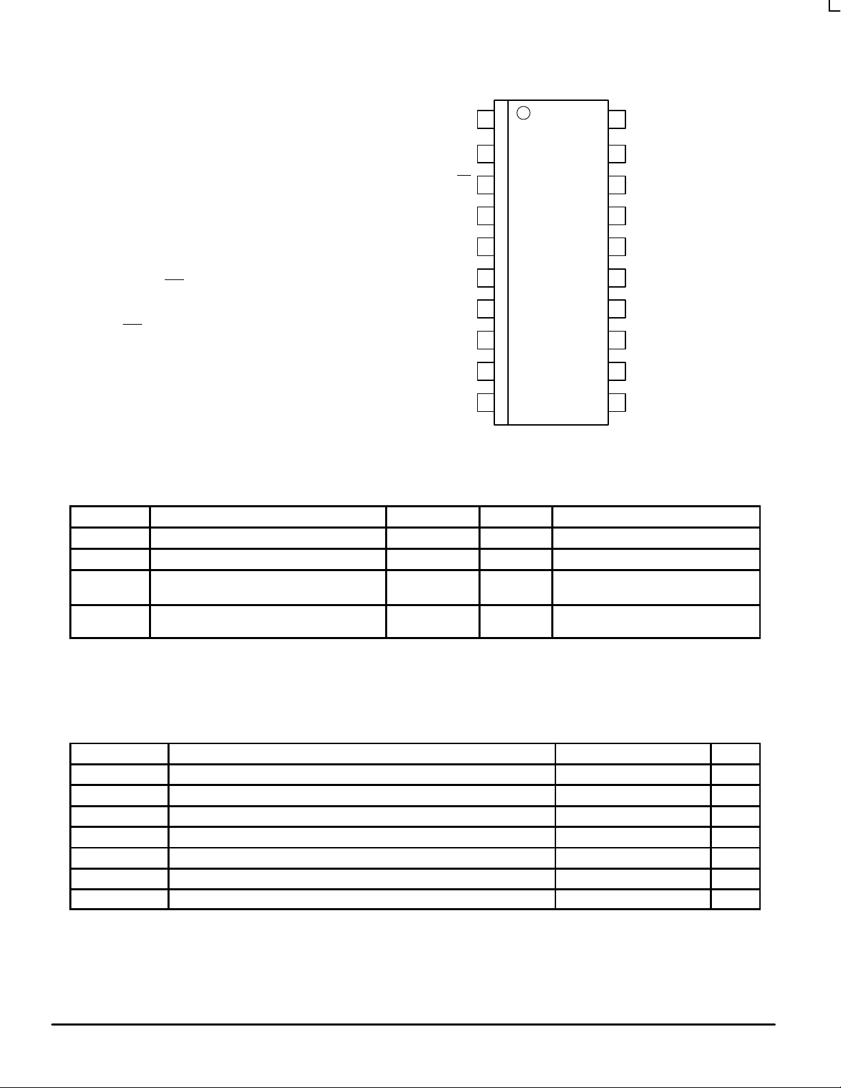
MC88921
20
19
18
GNDQ3
2X_QV
Q/2MR
Power–Down Mode Functionality
CC
1
2
3
The MC88921 has a special feature
designed in to allow the processor clock
PLL_EN
4
17
V
CC
inputs to be reset for total processor
power–down, and then to return to
5
16
Q2VCC(AN)
phase–locked operation very quickly when
the processor is powered–up again.
The MR
pin resets outputs 2X_Q, Q0
and Q1 only leaving the other outputs
6
7
15
14
GNDRC1
LOCKGND(AN)
operational for other system activity . When
MR
is negated, all outputs will be operating
normally within 3 clock cycles.
Q0
8
9
10
13
12
11
FBSELSYNC
Q1GND
V
CC
Pinout: 20–Lead Wide SOIC Package (Top View)
CAPACITANCE AND POWER SPECIFICATIONS
Symbol Parameter Value Typ Unit Test Conditions
C
C
PD
PD
IN
PD
1
2
Input Capacitance 4.5 pF VCC = 5.0V
Power Dissipation Capacitance 40 pF VCC = 5.0V
Power Dissipation at 33MHz With 50Ω
Thevenin Termination
Power Dissipation at 33MHz With 50Ω
Parallel Termination to GND
15mW/Output
90mW/Device
37.5mW/Output
225mW/Device
mW VCC = 5.0V
T = 25°C
mW VCC = 5.0V
T = 25°C
MAXIMUM RATINGS*
Symbol Parameter Limits Unit
VCC, AV
V
V
I
I
I
T
* Maximum Ratings are those values beyond which damage to the device may occur. Functional operation should be restricted to the
Recommended Operating Conditions.
MOTOROLA TIMING SOLUTIONS
CC
in
out
in
out
CC
stg
DC Supply Voltage Referenced to GND –0.5 to 7.0 V
DC Input Voltage (Referenced to GND) –0.5 to VCC +0.5 V
DC Output Voltage (Referenced to GND) –0.5 to VCC +0.5 V
DC Input Current, Per Pin ±20 mA
DC Output Sink/Source Current, Per Pin ±50 mA
DC VCC or GND Current Per Output Pin ±50 mA
Storage Temperature –65 to +150 °C
2
BR1333 — REV 5
Page 3
MC88921
RECOMMENDED OPERATING CONDITIONS
Symbol Parameter Limits Unit
V
CC
V
in
V
out
T
A
ESD Static Discharge Voltage > 1500 V
DC CHARACTERISTICS (TA = –40°C to 85°C; VCC = 5.0V ± 5%)
Supply Voltage 5.0 ±10% V
DC Input Voltage 0 to V
DC Output Voltage 0 to V
Ambient Operating Temperature 0 to 70 °C
CC
CC
V
V
Symbol Parameter V
V
IH
V
IL
V
OH
V
OL
I
IN
I
CCT
I
OLD
I
OHD
I
CC
1. IOL is +12mA for the LOCK output.
2. The PLL_EN input pin is not guaranteed to meet this specification.
3. Maximum test duration 2.0ms, one output loaded at a time.
Minimum High Level Input Voltage 4.75
Minimum Low Level Input Voltage 4.75
Minimum High Level Output Voltage 4.75
Minimum Low Level Output Voltage 4.75
Maximum Input Leakage Current 5.25 ±1.0 µA VI = VCC, GND
Maximum ICC/Input 5.25 2.0
Minimum Dynamic3 Output Current 5.25 88 mA V
Maximum Quiescent Supply Current 5.25 750 µA VI = VCC, GND
CC
5.25
5.25
5.25
5.25
5.25 –88 mA V
Guaranteed Limits Unit Condition
2.0
2.0
0.8
0.8
4.01
4.51
0.44
0.44
2
V V
V V
V VIN = VIH or V
V VIN = VIH or V
mA VI = VCC – 2.1V
SYNC INPUT TIMING REQUIREMENTS
Symbol Parameter Minimum Maximum Unit
t
RISE/FALL
SYNC Input
t
,
CYCLE
SYNC Input
Duty Cycle Duty Cycle, SYNC Input 50% ± 25%
Rise/Fall Time, SYNC Input
From 0.8V to 2.0V
Input Clock Period
SYNC Input
— 5.0 ns
1
f
ń
4
2X_Q
= 0.1V or
OUT
VCC – 0.1V
= 0.1V or
OUT
VCC – 0.1V
I
OH –36mA
I
OH +36mA
OLD
OHD
–36mA
+36mA
= 1.0V Max
= 3.85 Min
200 ns
IL
IL
1
TIMING SOLUTIONS
BR1333 — REV 5
3 MOTOROLA
Page 4

MC88921
LOCK
2X_Q
LOCK INDICAT OR
SYNC1
PLL_EN
MR
FBSEL
PFD
POWER–ON
RESET
CH
PUMP
01
RC1
VCO
D Q0
D Q1
D Q2
÷
2
D
D Q3
D
Q
R
Q
R
Q
R
Q
Q
R
Q
R
Q
“Dummy” Flip–Flop to Maintain
Phase–Locked Operation
Q/2
0
1
R
Figure 1. MC88921 Logic Block Diagram
FREQUENCY SPECIFICATIONS (TA = –40°C to 85°C; VCC = 5.0V ± 5%)
Symbol Parameter Guaranteed Minimum Unit
Fmax (2X_Q) Maximum Operating Frequency, 2X_Q Output 66 MHz
Fmax (‘Q’) Maximum Operating Frequency,
Q0–Q3 Outputs
1. Maximum Operating Frequency is guaranteed with the 88921 in a phase–locked condition, and all outputs loaded at 50pF.
33 MHz
MOTOROLA TIMING SOLUTIONS
4
BR1333 — REV 5
Page 5

MC88921
AC CHARACTERISTICS (TA = –40°C to 85°C; VCC = 5.0V ± 5%)
Symbol Parameter Minimum Maximum Unit Condition
t
RISE/FALL
All Outputs
t
RISE/FALL
2X_Q Output
t
pulse width(a)
(Q0, Q1, Q2, Q3)
t
pulse width(b)
(2X_Q Output)
t
PD
SYNC – Q/2
t
SKEWr
(Rising)
t
SKEWf
(Falling)
t
SKEWall
t
LOCK
t
PHL
t
REC
SYNC
t
REC
Normal Operation
tW, MR LOW
1. These specifications are not tested, they are guaranteed by statistical characterization. See Application Note 1 for a discussion of this
methodology.
2. Under equally loaded conditions and at a fixed temperature and voltage.
3. With VCC fully powered–on: t
4. See Application Note 4 for the distribution in time of each output referenced to SYNC.
5. Refer to Application Note 3 to translate signals to a 1.5V threshold.
6. Specification is valid only when the PLL_EN pin is low.
7. This is a typical specification only, worst case guarantees are not provided.
1
1
1,4
1,2
1,2
1,2
3
MR – Q Propagation Delay,
, MR to
6
, MR to
6
Rise/Fall Time, All Outputs into 50Ω
Load
Rise/Fall Time into a 20pF Load, With
Termination Specified in AppNote 3
1
Output Pulse Width
Q0, Q1, Q2, Q3 at VCC/2
1
Output Pulse Width
2X_Q at VCC/2
SYNC Input to Q Output Delay
(Measured at SYNC and Q/2 Pins)
Output–to–Output Skew
Between Outputs Q0–Q3
(Rising Edge Only)
Output–to–Output Skew
Between Outputs Q0–Q3
(Falling Edge Only)
Output–to–Output Skew
2X_Q, Q0–Q3 Rising
Phase–Lock Acquisition Time,
All Outputs to SYNC Input
MR
to Any Output (High–Low)
Reset Recovery Time rising MR edge
to falling SYNC edge
Recovery Time for Outputs 2X_Q, Q0,
Q1 to Return to Normal PLL Operation
Minimum Pulse Width, MR input Low 5 — ns
CLOCK
Max is with C1 = 0.1µF; t
0.3 1.6 ns t
0.5 1.6 ns t
0.5t
cycle
0.5t
cycle
–0.75 –0.15 ns With 1MΩ From RC1
+1.25
Min is with C1 = 0.01µF.
LOCK
5
– 0.5
– 0.5
7
— 500 ps Into a 50Ω Load
— 1.0 ns Into a 50Ω Load
— 1.0 ns Into a 50Ω Load
1 10 ms
1.5 13.5 ns Into a 50Ω Load
9 — ns
— 3 Clock Cycles
0.5t
5
0.5t
+ 0.55ns 50Ω Load Terminated to
cycle
+ 0.55ns 50Ω Load Terminated to
cycle
7
+3.25
(Q Frequency)
RISE
t
FALL
RISE
t
FALL
VCC/2 (See Application
Note 3)
VCC/2 (See Application
Note 3)
to An V
(See Application Note 2)
ns With 1MΩ From RC1
to An GND
(See Application Note 2)
Terminated to VCC/2
(See Timing Diagram in
Figure 6)
Terminated to VCC/2
(See Timing Diagram in
Figure 6)
Terminated to VCC/2
(See Timing Diagram in
Figure 6)
Terminated to VCC/2
ns
– 0.8V to 2.0V
– 2.0V to 0.8V
– 0.8V to 2.0V
– 2.0V to 0.8V
CC
TIMING SOLUTIONS
BR1333 — REV 5
5 MOTOROLA
Page 6

MC88921
Application Notes
1. Several specifications can only be measured when the
MC88921 is in phase–locked operation. It is not possible
to have the part in phase–lock on ATE (automated test
equipment). Statistical characterization techniques were
used to guarantee those specifications which cannot be
measured on the ATE. MC88921 units were fabricated
with key transistor properties intentionally varied to create
a 14 cell designed experimental matrix. IC performance
was characterized over a range of transistor properties
(represented by the 14 cells) in excess of the expected
process variation of the wafer fabrication area.
2. A 1MΩ resistor tied to either Analog VCC or Analog GND,
as shown in Figure 2, is required to ensure no jitter is
present on the MC88921 outputs. This technique causes
a phase offset between the SYNC input and the Q0
output, measured at the pins. The tPD spec describes how
this offset varies with process, temperature, and voltage.
The specs were arrived at by measuring the phase
relationship for the 14 lots described in note 1 while the
part was in phase–locked operation. The actual
measurements were made with a 10MHz SYNC input
(1.0ns edge rate from 0.8V to 2.0V). The phase
measurements were made at 1.5V. See Figure 2 for a
graphical description.
3. Two specs (t
RISE/FALL
and t
Width 2X_Q output,
PULSE
see AC Specifications) guarantee that the MC88921
meets the 20MHz, 25MHz and 33MHz 68040 P–Clock
input specification (at 40MHz, 50MHz, and 66MHz). For
these two specs to be guaranteed by Motorola, the
termination scheme shown in Figure 3 must be used. For
applications which require 1.5V thresholds, but do not
require a tight duty cycle the RP resistor can be ignored.
4. The tPD spec (SYNC to Q/2) guarantees how close the
Q/2 output will be locked to the reference input connected
to the SYNC input (including temperature and voltage
variation). This also tells what the skew from the Q/2
output on one part connected to a given reference input, to
the Q/2 output on one or more parts connected to that
reference input (assuming equal delay from the reference
input to the SYNC input of each part). Therefore the t
PD
spec is equivalent to a part–to–part specification.
However, to correctly predict the skew from a given output
on one part to any other output on one or more other parts,
the distribution of each output in relation to the SYNC
input must be known. This distribution for the MC88921 is
provided in Table 1.
TABLE 1. Distribution of Each Output versus SYNC
Output –(ps) +(ps)
2X_Q
Q0
Q1
Q2
Q3
Q/2
TBD
TBD
TBD
TBD
TBD
TBD
TBD
TBD
TBD
TBD
TBD
TBD
RC1
EXTERNAL
LOOP FILTER
WITH THE 1M
SPECIFICA TION, MEASURED AT THE INPUT PINS IS:
Ω
tPD = 2.25ns
SYNC INPUT
Q0 OUTPUT
330
Ω
R2
0.1µF
RESISTOR TIED IN THIS FASHION THE T
±
1.0ns (TYPICAL VALUES)
2.25ns
OFFSET
C1
ANALOG GND
1M
REFERENCE
RESISTOR
3V
Figure 2. Depiction of the Fixed SYNC to Q0 Offset (tPD) Which Is Present
When a 1MΩ Resistor Is Tied to VCC or Ground
5V
PD
ANALOG V
REFERENCE
WITH THE 1M
SPECIFICA TION, MEASURED AT THE INPUT PINS IS:
Ω
SYNC INPUT
Q0 OUTPUT
1M
RESISTOR
RESISTOR TIED IN THIS FASHION THE T
tPD = –0.80ns
CC
RC1
330
Ω
R2
0.1µF
ANALOG GND
±
0.30ns
–0.8ns
OFFSET
C1
5V
PD
3V
MOTOROLA TIMING SOLUTIONS
6
BR1333 — REV 5
Page 7

Zo (CLOCK
Ω
TRACE)
R
P
68040
P–CLOC
K
INPUT
RP = 1.5Zo
88921
2X_Q
OUTPUT
Rs
Rs = Zo – 7
Figure 3. MC68040 P–Clock Input T ermination Scheme
MC88921
Figure 4. Logical Representation of the MC88921 With Input/Output Frequency Relationships
SYNC Input
16.5MHz
CRYSTAL
OSCILLA TOR
t
SKEWall
t
SKEWf
SYNC
MR
PLL_EN
t
CYCLE
2X_Q
Q0
Q1
Q2
Q3
SYNC Input
t
SKEWr
66MHz P–CLOCK OUT-
PUT
33MHz
B–CLOCK
AND SYSTEM
OUTPUTS
t
SKEWf
t
SKEWr
Q0–Q3 Outputs
2X_Q Output
Figure 5. Output/Input Switching Waveforms and Timing Relationships
Timing Notes
1. The MC88921 aligns rising edges of the outputs and the SYNC input, therefore the SYNC input does not require a 50%
duty cycle.
2. All skew specs are measured between the VCC/2 crossing point of the appropriate output edges. All skews are specified as
‘windows’, not as a ± deviation around a center point.
TIMING SOLUTIONS
BR1333 — REV 5
7 MOTOROLA
Page 8

MC88921
The tPD spec includes the full temperature range from 0°C
to 70°C and the full VCC range from 4.75V to 5.25V . If the
∆T and ∆VCC is a given system are less than the
specification limits, the tPD spec window will be reduced.
Notes Concerning Loop Filter and Board Layout Issues
1. Figure 7 shows a loop filter and analog isolation scheme
which will be effective in most applications. The following
guidelines should be followed to ensure stable and
jitter–free operation:
1a. All loop filter and analog isolation components should be
tied as close to the package as possible. Stray current
passing through the parasitics of long traces can cause
undesirable voltage transients at the RC1 pin.
1b. The 47Ω resistors, the 10µF low frequency bypass
capacitor, and the 0.1µF high frequency bypass capacitor
form a wide bandwidth filter that will make the 88921 PLL
insensitive to voltage transients from the system digital
VCC supply and ground planes. This filter will typically
ensure that a 100mV step deviation on the digital V
supply will cause no more than a 100ps phase deviation
on the 88921 outputs. A 250mV step deviation on V
using the recommended filter values will cause no more
than a 250ps phase deviation; if a 25µF bypass capacitor
is used (instead of 10µF) a 250mV VCC step will cause no
more than a 100ps phase deviation.
If good bypass techniques are used on a board design
near components which may cause digital VCC and
ground noise, the above described VCC step deviations
should not occur at the 88921’s digital VCC supply. The
CC
CC
The tPD window for a given ∆T and ∆VCC is given by the
following regression formula:
TBD
purpose of the bypass filtering scheme shown in Figure 7
is to give the 88921 additional protection from the power
supply and ground plane transients that can occur in a
high frequency, high speed digital system.
1c. There are no special requirements set forth for the loop
filter resistors (1M and 330Ω). The loop filter capacitor
(0.1uF) can be a ceramic chip capacitor, the same as a
standard bypass capacitor.
1d. The 1M reference resistor injects current into the internal
charge pump of the PLL, causing a fixed offset between
the outputs and the SYNC input. This also prevents
excessive jitter caused by inherent PLL dead–band. If the
VCO (2X_Q output) is running above 40MHz, the 1M
resistor provides the correct amount of current injection
into the charge pump (2–3µA).
2. In addition to the bypass capacitors used in the analog
filter of Figure 7, there should be a 0.1µF bypass
capacitor between each of the other (digital) four V
CC
pins and the board ground plane. This will reduce output
switching noise caused by the 88921 outputs, in addition
to reducing potential for noise in the ‘analog’ section of
the chip. These bypass capacitors should also be tied as
close to the 88921 package as possible.
BOARD V
CC
47
Ω
5
10µF LOW
FREQ BIAS
0.1µF HIGH
FREQ BIAS
1M
Ω
Ω
47
BOARD GND
ANALOG V
Ω
330
6
RC1
0.1µF (LOOP
FILTER CAP)
A SEPARATE ANALOG POWER SUPPLY IS NOT NECESSARY AND
SHOULD NOT BE USED. FOLLOWING THESE PRESCRIBED GUIDELINES IS ALL THAT IS NECESSAR Y TO USE THE MC88921 IN A NORMAL
DIGITAL ENVIRONMENT.
7
ANALOG GND
CC
ANALOG LOOP FILTER/VCO
SECTION OF THE MC88921
20–PIN SOIC PACKAGE (NOT
DRAWN TO SCALE)
Figure 6. Recommended Loop Filter and Analog Isolation Scheme for the MC88921
MOTOROLA TIMING SOLUTIONS
8
BR1333 — REV 5
Page 9

MC88921
Pentium
Microprocessor
PCLK
MEMORY MODULE
16.5MHz
X–TAL
OSCILLA TOR
SYNC
2X_Q
Q1
Q2
Q3
66MHz
33MHz
Figure 7. T ypical MC88921/Pentium Microprocessor System Configuration
ASIC
ASIC
TIMING SOLUTIONS
BR1333 — REV 5
9 MOTOROLA
Page 10

MC88921
-T-
1
G
0.25 (0.010)MT
OUTLINE DIMENSIONS
DW SUFFIX
SOIC PACKAGE
CASE 751D-03
NOTES:
-A-
1120
-B-
P
0.25 (0.010) B
10
10 PL
MM
R X 45°
C
SEATING
PLANE
D
20 PL
B
K
S
S
A
M
F
J
1. DIMENSIONING AND TOLERANCING PER ANSI
Y14.5M, 1982.
2. CONTROLLING DIMENSION: MILLIMETER.
3. DIMENSION A AND B DO NOT INCLUDE MOLD
PROTRUSION.
4. MAXIMUM MOLD PROTRUSION 0.15 (0.006) PER
SIDE.
5. 751D-01, AND -02 OBSOLETE, NEW STANDARD
751D-03.
MILLIMETERS INCHES
MIN MINMAX MAX
DIM
12.95
12.65
A
B
C
D
F
G
K
M
P
R
7.60
7.40
2.65
2.35
0.49
0.35
0.90
0.50
1.27 BSC 0.050 BSC
J
0.32
0.25
0.25
0.10
7
0
°
0.25
10.55
0.75
°
10.05
0.499
0.292
0.093
0.014
0.020
0.010
0.004
0
0.395
0.010
0.510
0.299
0.104
0.019
0.035
0.012
0.009
7
°
°
0.415
0.029
Motorola reserves the right to make changes without further notice to any products herein. Motorola makes no warranty , representation or guarantee regarding
the suitability of its products for any particular purpose, nor does Motorola assume any liability arising out of the application or use of any product or circuit,
and specifically disclaims any and all liability, including without limitation consequential or incidental damages. “T ypical” parameters can and do vary in different
applications. All operating parameters, including “T ypicals” must be validated for each customer application by customer’s technical experts. Motorola does
not convey any license under its patent rights nor the rights of others. Motorola products are not designed, intended, or authorized for use as components in
systems intended for surgical implant into the body, or other applications intended to support or sustain life, or for any other application in which the failure of
the Motorola product could create a situation where personal injury or death may occur. Should Buyer purchase or use Motorola products for any such
unintended or unauthorized application, Buyer shall indemnify and hold Motorola and its officers, employees, subsidiaries, affiliates, and distributors harmless
against all claims, costs, damages, and expenses, and reasonable attorney fees arising out of, directly or indirectly, any claim of personal injury or death
associated with such unintended or unauthorized use, even if such claim alleges that Motorola was negligent regarding the design or manufacture of the part.
Motorola and are registered trademarks of Motorola, Inc. Motorola, Inc. is an Equal Opportunity/Affirmative Action Employer.
How to reach us:
USA/EUROPE: Motorola Literature Distribution; JAPAN: Nippon Motorola Ltd.; Tatsumi–SPD–JLDC, Toshikatsu Otsuki,
P.O. Box 20912; Phoenix, Arizona 85036. 1–800–441–2447 6F Seibu–Butsuryu–Center, 3–14–2 Tatsumi Koto–Ku, Tokyo 135, Japan. 03–3521–8315
MFAX: RMFAX0@email.sps.mot.com –TOUCHTONE (602) 244–6609 HONG KONG: Motorola Semiconductors H.K. Ltd.; 8B Tai Ping Industrial Park,
INTERNET: http://Design–NET .com 51 Ting Kok Road, Tai Po, N.T ., Hong Kong. 852–26629298
MOTOROLA TIMING SOLUTIONS
◊
CODELINE
10
*MC88921/D*
MC88921/D
BR1333 — REV 5
 Loading...