

Page 1
SEMICONDUCTOR TECHNICAL DATA
The MC88913 is a high–speed, low power, hex divide–by–two D–type
flip–flop with two inverting and four non–inverting outputs that have
closely matched propagation delays. With a TTL compatible buffered
clock input that is common to all flip–flops, the MC88913 is ideal for use in
high–frequency systems as a clock driver, providing multiple outputs that
are synchronous.
Order this document
from Logic Marketing
LOW SKEW CMOS
CLOCK DRIVER
• Minimum Clock Input f
MAX
of 1 10MHz
• TTL Compatible Positive Edge–Triggered Clock
• Matched Outputs for Synchronous Applications
• Outputs Source/Sink 24mA
• Part–to–Part Skew of Less Than 4.0ns
• Guaranteed Rise and Fall Times for a Given Capacitive Load
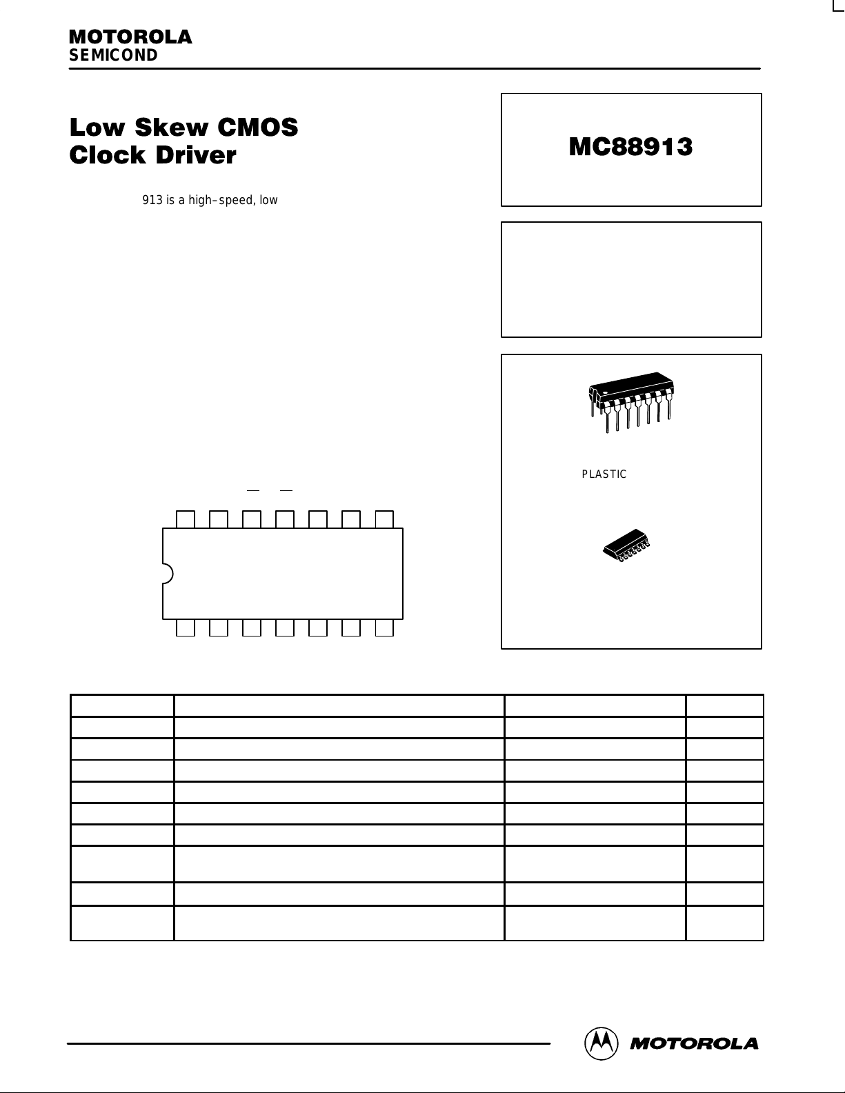
Pinout: 14–Lead Plastic (Top View)
V
GND
Q
Q
Q
GND
9
6
GND
GND
8
7
GND
SOIC Package**
5
12
Q
4
3
11
10
3
4
5
Q
0
Q
1
2
CC
14
1
GND
13
2
CLK
MAXIMUM RATINGS*
Symbol
V
CC
V
in
V
out
I
in
I
out
I
CC
P
D
T
stg
T
L
* Maximum Ratings are those values beyond which damage to the device may occur. Functional operation should be restricted to the
Recommended Operating Conditions.
** Derating: Plastic Package: –10mW/°C from 65°C to 125°C
DC Supply Voltage (Referenced to GND) –0.5 to +7.0 V
DC Input Voltage (Referenced to GND) –0.5 to VCC + 0.5 V
DC Output Voltage (Referenced to GND) –0.5 to VCC + 0.5 V
DC Input Current, per Pin ± 20 mA
DC Output Sink/Source Current, per Pin ± 50 mA
DC VCC or GND Current per Output Pin ± 50 mA
Power Dissipation in Still Air Plastic Package**
Storage Temperature –65 to +150 °C
Lead Temperature, 1mm from Case for 10s (Plastic or SOIC
Package)
SOIC Package: –7.0mW/°C from 65°C to 125°C
Parameter Value Units
14
1
N SUFFIX
PLASTIC PACKAGE
CASE 646–06
14
1
D SUFFIX
PLASTIC PACKAGE
CASE 751A–03
750
500
260 °C
mW
11/93
Motorola, Inc. 1995
1
REV 3
Page 2
MC88913
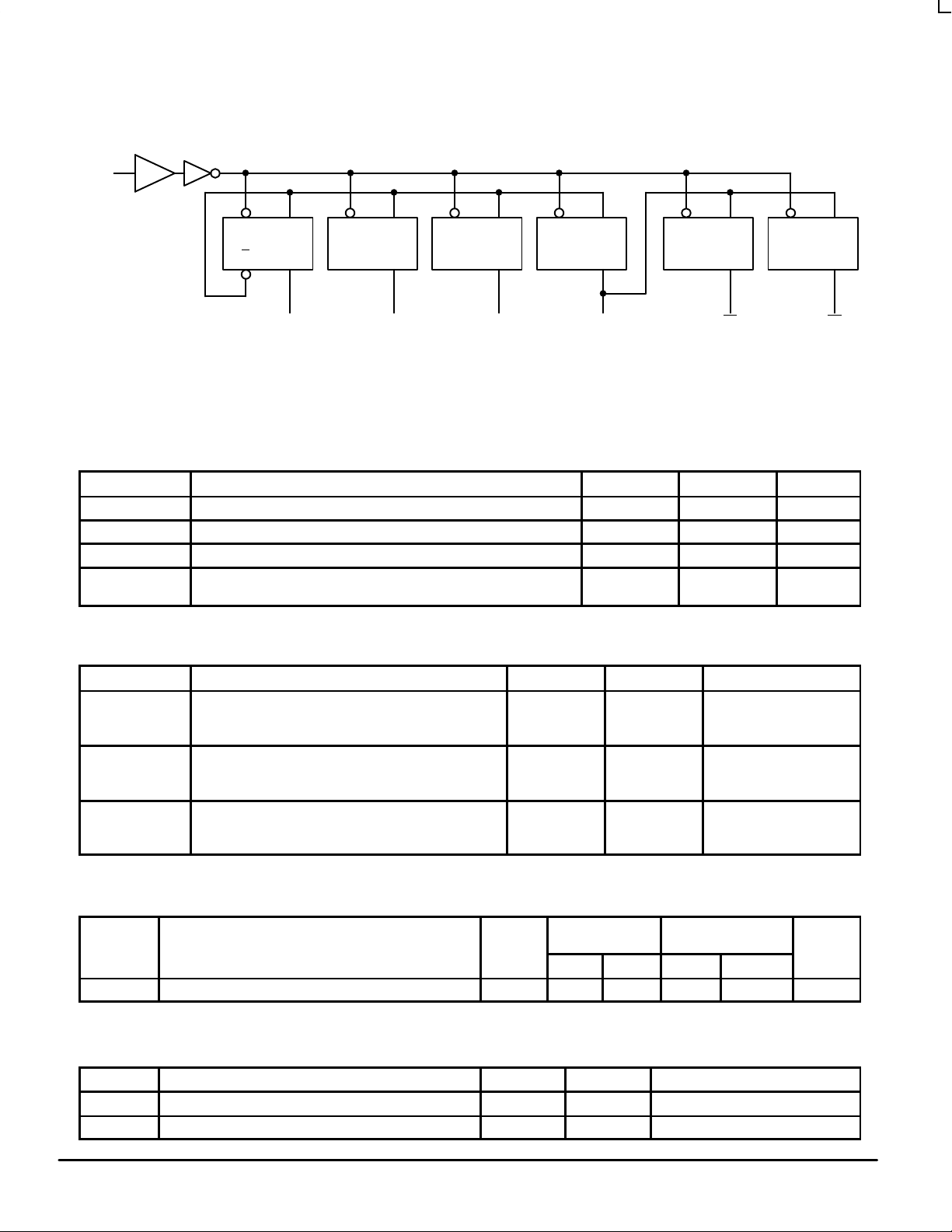
CLK
LOGIC DIAGRAM
CLKQD
Q
Q
0
NOTE: This diagram is provided only for understanding of logic operation and should not be used to estimate propagation delays
CLK D
Q
Q
1
RECOMMENDED OPERATING CONDITIONS
Parameter Min Max Unit
V
meas
V
CC
Vin, V
T
A
tr, t
f
Symbol
out
DC Supply Voltage (Referenced to GND) 2.0 6.0 V
DC Input Voltage, Output Voltage (Referenced to GND) 0 V
Operating Temperature –40 +85 °C
Input Rise and Fall Time Vin from 0.8 to 2.0V
DC CHARACTERISTICS (unless otherwise specified)
Parameter Unit Condition
I
CC
I
CC
I
CCT
Symbol
Maximum Quiescent Supply Current 80 µA VIN = VCC or GND
Maximum Quiescent Supply Current 8.0 µA VIN = VCC or GND
Maximum Additional ICC/Input 1.5 mA VIN = VCC –2.1V
CLK D
from 0.8 to 2.0V
CLK D
Q
Q
2
Q
Q
3
0
0
CLK D
8.0
VCC = 5.5V,
TA = Worst Case
VCC = 5.5V,
TA = 25°C
VCC = 5.5V,
TA = Worst Case
Q
Q
CC
10
CLK D
Q
V
ns/V
Q
5
4
AC OPERATING REQUIREMENTS
TA = 25°C
CL = 50 pF
Symbol Parameter VCC (V) Min Max Min Max Unit
t
W
CLK Pulse Width (HIGH to LOW) 5.0 3.0 3.0 ns
TA = –40 to +85°C
CL = 50 pF
CAPACITANCE
Symbol
C
IN
C
PD
MOTOROLA TIMING SOLUTIONS
Input Capacitance 4.5 pF VCC = 5.0V
Power Dissipation Capacitance 30 pF VCC = 5.0V
Parameter Typ Unit Condition
2
BR1333 — REV 5
Page 3

DC CHARACTERISTICS
Symbol Parameter V
V
IH
V
IL
V
OH
V
OL
I
IN
I
CCT
I
OLD
I
OHD
* All outputs loaded; thresholds on inputs associated with output under test.
** Maximum test duration 20ms, one output at a time.
Minimum High Level
Input Voltage
Maximum Low Level
Input Voltage
Minimum High Level 4.5
Maximum Low Level
Output Voltage
Maximum Input 5.5 ±0.1 ±0.1 µA VI = VCC, GND
Maximum ICC/Input 5.5 0.6 1.5 mA VI = VCC –2.1V
Minimum Dynamic Output Current** 5.5 75 mA V
CC
4.5
5.5
4.5
5.5
5.5
4.5
5.5
4.5
5.5
4.5
5.5
5.5 –75 mA V
MC88913
TA =
2.0
2.0
0.8
0.8
4.4
5.4
0.1
0.1
–40 to +85°C
2.0
2.0
0.8
0.8
4.4
5.4
3.76
4.76
0.1
0.1
0.44
0.44
V V
V V
V I
V *VIN = VIL or V
V I
V *VIN = VIL or V
= 0.1V or
OUT
VCC – 0.1V
= 0.1V or
OUT
VCC – 0.1V
= –50µA
OUT
IOH = –24mA
–24mA
= 50µA
OUT
IOH = 24mA
24mA
= 1.65V
OLD
= 3.85V
OHD
TA = +25°C
Typ Guaranteed Max Unit Conditions
1.5
1.5
1.5
1.5
4.49
5.49
3.86
4.86
0.001
0.001
0.36
0.36
IH
IH
AC CHARACTERISTICS (VCC = 5.0V ±10%)
TA = 25°C
CL = 50 pF
Symbol Parameter VCC (V) Min Max Min Max Unit
f
MAX
t
,
PLH
t
PHL
t
PV
t
PS
t
OS
t
rise
t
fall
1. For a given set of conditions (i.e., capacitive load, temperature and VCC) the variation from device to device is guaranteed to be less than or equal to the maximum.
2. Where tp Qn and tp Qm are the actual propagation delays (any combination of HIGH or LOW) for any two separate outputs from a given high transition of CLK.
Maximum Clock Frequency (50% Duty Cycle) 5.0 110 110 MHz
Propagation Delay
CLK to Qn, Q
Propagation Delay Variation
CLK to Q0, Q1, Q2 (see Note 1)
Propagation Delay Variation
CLK to All Outputs (see Note 1)
Propagation Delay Skew (Q0, Q1, Q2)
|t
PHL
Propagation Delay Skew (All Outputs)
|t
PHL
Output–to–Output Skew (Q0, Q1, Q2)
|tp Qn – tp Qm| (see Note 2)
Output–to–Output Skew (All Outputs)
|tp Qn – tp Qm| (see Note 2)
Rise/Fall Time for Q0, Q1, Q
(0.2 x VCC to 0.8 x VCC)
Rise/Fall Time for All Outputs
(0.2 x VCC to 0.8 x VCC)
Actual – t
Actual – t
n
Actual|
PLH
Actual|
PLH
2
5.0 4.0 10.5 4.0 11.5 ns
5.0 4.0 5.0 ns
5.0 4.5 5.5 ns
5.0 1.0 1.0 ns
5.0 1.5 1.5 ns
5.0 1.0 1.0 ns
5.0 1.5 1.5 ns
5.0 3.0 4.0 ns
5.0 3.5 4.5 ns
TA = –40 to +85°C
CL = 50 pF
TIMING SOLUTIONS
BR1333 — REV 5
3 MOTOROLA
Page 4

MC88913
SEATING
PLANE
OUTLINE DIMENSIONS
PLASTIC PACKAGE
14 8
B
17
A
F
C
N
SEATING
HG D
–A
–
PLANE
814
–B–P 7 PL
1
7
G
D 14 PL
0.25 (0.010) T B A
M
K
K
PLASTIC SOIC PACKAGE
C
S S
R
N SUFFIX
CASE 646–06
ISSUE L
L
J
M
D SUFFIX
CASE 751A–03
ISSUE F
M M
B0.25 (0.010)
X 45°
M
NOTES:
1. LEADS WITHIN 0.13 (0.005) RADIUS OF TRUE
POSITION AT SEATING PLANE AT MAXIMUM
MATERIAL CONDITION.
2. DIMENSION L TO CENTER OF LEADS WHEN
FORMED PARALLEL.
3. DIMENSION B DOES NOT INCLUDE MOLD
FLASH.
4. ROUNDED CORNERS OPTIONAL.
INCHES MILLIMETERS
MIN MINMAX MAX
DIM
0.715
A
0.240
B
0.145
C
0.015
D
0.040
F
G
0.100 BSC
0.052
H
0.008
J
0.115
K
L
0.300 BSC
°
0
M
0.015
N
NOTES:
1. DIMENSIONING AND TOLERANCING PER ANSI
Y14.5M, 1982.
2. CONTROLLING DIMENSION: MILLIMETER.
3. DIMENSIONS A AND B DO NOT INCLUDE
MOLD PROTRUSION.
4. MAXIMUM MOLD PROTRUSION 0.15 (0.006)
PER SIDE.
5. DIMENSION D DOES NOT INCLUDE DAMBAR
PROTRUSION. ALLOWABLE DAMBAR
PROTRUSION SHALL BE 0.127 (0.005) TOTAL
IN EXCESS OF THE D DIMENSION AT
MAXIMUM MATERIAL CONDITION.
F
J
DIM
A
B
C
D
F
G
J
K
M
P
R
18.16
°
6.10
3.69
0.38
1.02
2.54 BSC
1.32
0.20
2.92
7.62 BSC
0°
0.39
8.75
4.00
1.75
0.49
1.25
0.25
0.25
7
°
6.20
0.50
19.56
0.770
0.260
0.185
0.021
0.070
0.095
0.015
0.135
°
10
0.039
MILLIMETERS INCHES
MIN MINMAX MAX
8.55
3.80
1.35
0.35
0.40
1.27 BSC 0.050 BSC
0.19
0.10
0
5.80
0.25
6.60
4.69
0.53
1.78
2.41
0.38
3.43
10
1.01
0.337
0.150
0.054
0.014
0.016
0.008
0.004
0.228
0.010
°
0.344
0.157
0.068
0.019
0.049
0.009
0.009
7
0
°
°
0.244
0.019
Motorola reserves the right to make changes without further notice to any products herein. Motorola makes no warranty , representation or guarantee regarding
the suitability of its products for any particular purpose, nor does Motorola assume any liability arising out of the application or use of any product or circuit,
and specifically disclaims any and all liability, including without limitation consequential or incidental damages. “T ypical” parameters can and do vary in different
applications. All operating parameters, including “T ypicals” must be validated for each customer application by customer’s technical experts. Motorola does
not convey any license under its patent rights nor the rights of others. Motorola products are not designed, intended, or authorized for use as components in
systems intended for surgical implant into the body, or other applications intended to support or sustain life, or for any other application in which the failure of
the Motorola product could create a situation where personal injury or death may occur. Should Buyer purchase or use Motorola products for any such
unintended or unauthorized application, Buyer shall indemnify and hold Motorola and its officers, employees, subsidiaries, affiliates, and distributors harmless
against all claims, costs, damages, and expenses, and reasonable attorney fees arising out of, directly or indirectly, any claim of personal injury or death
associated with such unintended or unauthorized use, even if such claim alleges that Motorola was negligent regarding the design or manufacture of the part.
Motorola and are registered trademarks of Motorola, Inc. Motorola, Inc. is an Equal Opportunity/Affirmative Action Employer .
How to reach us:
USA/EUROPE: Motorola Literature Distribution; JAPAN: Nippon Motorola Ltd.; Tatsumi–SPD–JLDC, Toshikatsu Otsuki,
P.O. Box 20912; Phoenix, Arizona 85036. 1–800–441–2447 6F Seibu–Butsuryu–Center, 3–14–2 Tatsumi Koto–Ku, Tokyo 135, Japan. 03–3521–8315
MFAX: RMFAX0@email.sps.mot.com –TOUCHTONE (602) 244–6609 HONG KONG: Motorola Semiconductors H.K. Ltd.; 8B Tai Ping Industrial Park,
INTERNET: http://Design–NET .com 51 Ting Kok Road, Tai Po, N.T., Hong Kong. 852–26629298
MOTOROLA TIMING SOLUTIONS
◊
CODELINE
4
*MC88913/D*
MC88913/D
BR1333 — REV 5
 Loading...