

Page 1
November 1989 Order Number: 271058-005
M80C86/M80C86-2
16-BIT CHMOS MICROPROCESSOR
MILITARY
Y
Pin-for-Pin and Functionally Compatible
to Industry Standard HMOS M8086
Y
Fully Static Design with Frequency
Range from D.C. to:
Ð 5 MHz for M80C86
Ð 8 MHz for M80C86-2
Y
Low Power Operation
Ð Operating I
CC
e
10 mA/MHz
Ð Standby I
CCS
e
500 mA max
Y
Bus-Hold Circuitry Eliminates Pull-Up
Resistors
Y
Direct Addressing Capability of
1 MByte of Memory
Y
Architecture Designed for Powerful
Assembly Language and Efficient High
Level Languages
Y
24 Operand Addressing Modes
Y
Byte, Word and Block Operations
Y
8 and 16-Bit Signed and Unsigned
Arithmetic
Ð Binary or Decimal
Ð Multiply and Divide
Y
Military Temperature Range:
b
55§Ctoa125§C(TC)
The Intel M80C86 is a high performance, CHMOS version of the industry standard HMOS M8086 16-bit CPU. It
is available in 5 and 8 MHz clock rates. The M80C86 offers two modes of operation: MINimum for small
systems and MAXimum for larger applications such as multiprocessing. It is available in 40-pin DIP package.
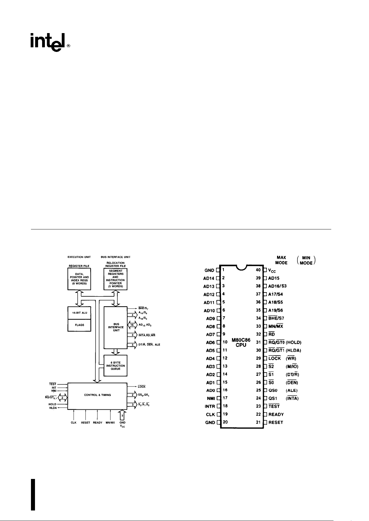
271058–1
Figure 1. M80C86 CPU Block Diagram
271058–2
Figure 2. M80C86 40-Lead DIP Configuration
Page 2
M80C86/M80C86-2
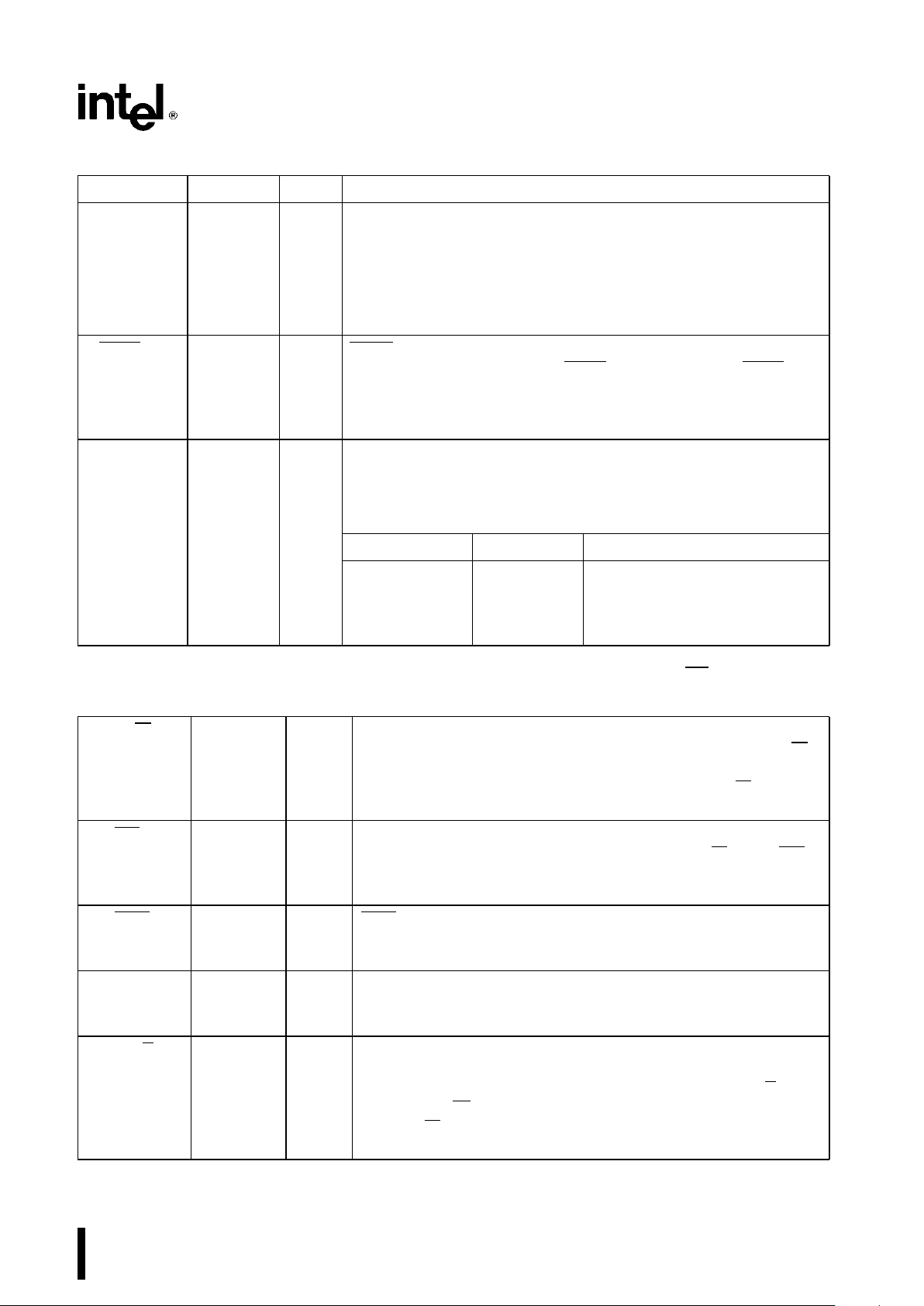
Table 1. Pin Description
The following pin function descriptions are for M80C86 systems in either minimum or maximum mode. The
‘‘Local Bus’’ in these descriptions is the direct multiplexed bus interface connection to the M80C86 (without
regard to additional bus buffers).
Symbol Pin No. Type Name and Function
AD15–AD
0
2– 16, 39 I/O ADDRESS DATA BUS: These lines constitute the time multiplexed
memory/IO address (T
1
) and data (T2,T3,TW,T4) bus. A0is
analogous to BHE
for the lower byte of the data bus, pins D7–D0.It
is LOW during T
1
when a byte is to be transferred on the lower
portion of the bus in memory or I/O operations. Eight-bit oriented
devices tied to the lower half would normally use A0to condition
chip select functions. (See BHE
.) These lines are active HIGH and
float to 3-state OFF
(1)
during interrupt acknowledge and local bus
‘‘hold acknowledge.’’
A19/S6, 35–38 O ADDRESS/STATUS: During T1these are the four most significant
A
18/S5
, address lines for memory operations. During I/O operations
A
17/S4
, these lines are LOW. During memory and I/O operations,
A16/S
3
status information is available on these lines during T2,T3,TW,
and T
4
. The status of the interrupt enable FLAG bit (S5) is updated
at the beginning of each CLK cycle. A
17/S4
and A16/S3are
encoded as shown.
This information indicates which relocation register is presently
being used for data accessing.
These lines float to 3-state OFF
(1)
during local bus ‘‘hold
acknowledge.’’
A17/S
4
A16/S
3
Characteristics
0 (LOW) 0 Alternate Data
0 1 Stack
1 (HIGH) 0 Code or None
1 1 Data
S
6
is 0
(LOW)
BHE/S
7
34 O BUS HIGH ENABLE/STATUS: During T1the bus high enable signal
(BHE
) should be used to enable data onto the most significant half
of the data bus, pins D
15–D8
. Eight-bit oriented devices tied to the
upper half of the bus would normally use BHE
to condition chip
select functions. BHE is LOW during T1for read, write, and interrupt
acknowledge cycles when a byte is to be transferred on the high
portion of the bus. The S
7
status information is available during T2,
T
3
, and T4. The signal is active LOW, and floats to 3-state OFF
(1)
in
‘‘hold.’’ It is LOW during T
1
for the first interrupt acknowledge cycle.
BHE A
0
Characteristics
0 0 Whole word
0 1 Upper byte from/
to odd address
1 0 Lower byte from/
to even address
1 1 None
2
Page 3
M80C86/M80C86-2
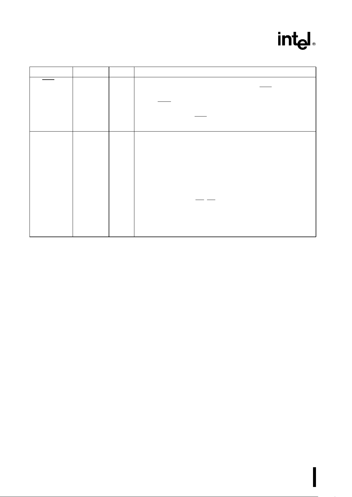
Table 1. Pin Description (Continued)
Symbol Pin No. Type Name and Function
RD 32 O READ: Read strobe indicates that the processor is performing a
memory of I/O read cycle, depending on the state of the S
2
pin.
This signal is used to read devices which reside on the M80C86
local bus. RD is active LOW during T2,T3and TWof any read cycle,
and is guaranteed to remain HIGH in T
2
until the M80C86 local bus
has floated.
This floats to 3-state OFF in ‘‘hold acknowledge.’’
READY 22 I READY: is the acknowledgement from the addressed memory or
I/O device that it will complete the data transfer. The READY signal
from memory/IO is synchronized by the M82C84A Clock Generator
to form READY. This signal is active HIGH. The M80C86 READY
input is not synchronized. Correct operation is not guaranteed if the
setup and hold times are not met.
INTR 18 I INTERRUPT REQUEST: is a level triggered input which is sampled
during the last clock cycle of each instruction to determine if the
processor should enter into an interrupt acknowledge operation. A
subroutine is vectored to via an interrupt vector lookup table
located in system memory. It can be internally masked by software
resetting the interrupt enable bit. INTR is internally synchronized.
This signal is active HIGH.
TEST 23 I TEST: input is examined by the ‘‘Wait’’ instruction. If the TEST input
is LOW execution continues, otherwise the processor waits in an
‘‘Idle’’ state. This input is synchronized internally during each clock
cycle on the leading edge of CLK.
NMI 17 I NON-MASKABLE INTERRUPT: an edge triggered input which
causes a type 2 interrupt. A subroutine is vectored to via an
interrupt vector lookup table located in system memory. NMI is not
maskable internally by software. A transition from a LOW to HIGH
initiates the interrupt at the end of the current instruction. This input
is internally synchronized.
RESET 21 I RESET: causes the processor to immediately terminate its present
activity. The signal must be active HIGH for at least four clock
cycles. It restarts execution, as described in the Instruction Set
description, when RESET returns LOW. RESET is internally
synchronized.
CLK 19 I CLOCK: provides the basic timing for the processor and bus
controller. It is asymmetric with a 33% duty cycle to provide
optimized internal timing.
V
CC
40 VCC:a5V power supply pin.
GND 1, 20 GROUND: Both must be connected.
MN/MX 33 I MINIMUM/MAXIMUM: indicates what mode the processor is to
operate in. The two modes are discussed in the following sections.
3
Page 4
M80C86/M80C86-2
Table 1. Pin Description (Continued)
The following pin function descriptions are for the M80C86/M82C88 system in maximum mode (i.e.,
MN/MX
e
VSS). Only the pin functions which are unique to maximum mode are described; all other pin func-
tions are as described above.
Symbol Pin No. Type Name and Function
S2,S1,S
0
26–28 O STATUS: active during T4,T1, and T2and is returned to the passive
state (1,1,1) during T
3
or during TWwhen READY is HIGH. This
status is used by the M82C88 Bus Controller to generate all memory
and I/O access control signals. Any change by S
2,S1,S0
during T
4
is used to indicate the beginning of a bus cycle, and the return to the
passive state in T3or TWis used to indicate the end of a bus cycle.
These signals float to 3-state OFF
(1)
in ‘‘hold acknowledge.’’ These
status lines are encoded as shown.
S
2
S
1
S
0
Characteristics
0 (LOW) 0 0 Interrupt
Acknowledge
0 0 1 Read I/O Port
0 1 0 Write I/O Port
0 1 1 Halt
1 (HIGH) 0 0 Code Access
1 0 1 Read Memory
1 1 0 Write Memory
1 1 1 Passive
RQ/GT
0,
30, 31 I/O REQUEST/GRANT: pins are used by other local bus masters to
RQ
/GT
1
force the processor to release the local bus at the end of the
processor’s current bus cycle. Each pin is bidirectional with RQ
/GT
0
having higher priority than RQ/GT1.RQ/GT has an internal pull-up
resistor so may be left unconnected. The request/grant sequence is
as follows (see timing diagram):
1. A pulse of 1 CLK wide from another local bus master indicates a
local bus request (‘‘hold’’) to the M80C86 (pulse 1).
2. During a T4or T1clock cycle, a pulse 1 CLK wide from the
M80C86 to the requesting master (pulse 2), indicates that the
M80C86 has allowed the local bus to float and that it will enter the
‘‘hold acknowledge’’ state at the next CLK. The CPU’s bus interface
unit is disconnected logically from the local bus during ‘‘hold
acknowledge.’’
3. A pulse 1 CLK wide from the requesting master indicates to the
M80C86 (pulse 3) that the ‘‘hold’’ request is about to end and that
M80C86 can reclaim the local bus at the next CLK.
Each master-master exchange of the local bus is a sequence of 3
pulses. There must be one dead CLK cycle after each bus exchange.
Pulses are active LOW.
If the request is made while the CPU is performing a memory cycle, it
will release the local bus during T
4
of the cycle when all the following
conditions are met:
1. Request occurs on or before T
2
.
2. Current cycle is not the low byte of a word (on an odd address).
3. Current cycle is not the first acknowledge of an interrupt
acknowledge sequence.
4. A locked instruction is not currently executing.
4
Page 5
M80C86/M80C86-2
Table 1. Pin Description (Continued)
Symbol Pin No. Type Name and Function
If the local bus is idle when the request is made the two possible
events will follow:
1. Local bus will be released during the next clock.
2. A memory cycle will start within 3 clocks. Now the four rules for a
currently active memory cycle apply with condition number 1 already
satisfied.
LOCK 29 O LOCK: output indicates that other system bus masters are not to gain
control of the system bus while LOCK
is active LOW. The LOCK
signal is activated by the ‘‘LOCK’’ prefix instruction and remains
active until the completion of the next instruction. This signal is active
LOW, and floats to 3-state OFF
(1)
in ‘‘hold acknowledge.’’
QS1,QS
0
24, 25 O QUEUE STATUS: The queue status is valid during the CLK cycle
after which the queue operation is performed.
QS
1
and QS0provide status to allow external tracking of the internal
M80C86 instruction queue.
QS
1
QS
0
Characteristics
0 (LOW) 0 No Operation
0 1 First Byte of Op Code from Queue
1 (HIGH) 0 Empty the Queue
1 1 Subsequent Byte from Queue
The following pin function descriptions are for the M80C86 in minimum mode (i.e., MN/MXeVCC). Only the
pin functions which are unique to minimum mode are described; all other pin functions are described above.
M/IO 28 O STATUS LINE: logically equivalent to S2in the maximum mode. It
is used to distinguish a memory access from an I/O access. M/IO
becomes valid in the T4preceding a bus cycle and remains valid
until the final T
4
of the cycle (MeHIGH, IOeLOW). M/IO floats to
3-state OFF
(1)
in local bus ‘‘hold acknowledge.’’
WR 29 O WRITE: indicates that the processor is performing a write memory
or write I/O cycle, depending on the state of the M/IO signal. WR is
active for T
2,T3
and TWof any write cycle. It is active LOW, and
floats to 3-state OFF
(1)
in local bus ‘‘hold acknowledge.’’
INTA 24 O INTA is used as a read strobe for interrupt acknowledge cycles. It is
active LOW during T
2,T3
and TWof each interrupt acknowledge
cycle.
ALE 25 O ADDRESS LATCH ENABLE: provided by the processor to latch
the address into an address latch. It is a HIGH pulse active during
T
1
of any bus cycle. Note that ALE is never floated.
DT/R 27 O DATA TRANSMIT/RECEIVE: needed in minimum system that
desires to use a data bus transceiver. It is used to control the
direction of data flow through the transceiver. Logically DT/R is
equivalent to S
1
in the maximum mode, and its timing is the same
as for M/IO.(TeHIGH, ReLOW.) This signal floats to 3-state
OFF
(1)
in local bus ‘‘hold acknowledge.’’
5
Page 6
M80C86/M80C86-2
Table 1. Pin Description (Continued)
Symbol Pin No. Type Name and Function
DEN 26 O DATA ENABLE: provided as an output enable for the transceiver in
a minimum system which uses the transceiver. DEN
is active LOW
during each memory and I/O access and for INTA cycles. For a
read or INTA cycle it is active from the middle of T2until the middle
of T
4
, while for a write cycle it is active from the beginning of T
2
until the middle of T4. DEN floats to 3-state OFF
(1)
in local bus
‘‘hold acknowledge.’’
HOLD, 31, 30 I/O HOLD: indicates that another master is requesting a local bus
HLDA ‘‘hold.’’ To be acknowledged, HOLD must be active HIGH. The
processor receiving the ‘‘hold’’ request will issue HLDA (HIGH) as
an acknowledgement in the middle of a T
1
clock cycle.
Simultaneous with the issuance of HLDA the processor will float the
local bus and control lines. After HOLD is detected as being LOW,
the processor will LOWer the HLDA, and when the processor
needs to run another cycle, it will again drive the local bus and
control lines.
The same rules as for RQ/GT apply regarding when the local bus
will be released.
HOLD is not an asynchronous input. External synchronization
should be provided if the system cannot otherwise guarantee the
setup time.
NOTE:
1. See the section on Bus Hold Circuitry.
FUNCTIONAL DESCRIPTION
STATIC OPERATION
All M80C86 circuitry is of static design. Internal registers, counters and latches are static and require no
refresh as with dynamic circuit design. This eliminates the minimum operating frequency restriction
placed on other microprocessors. The CMOS
M80C86 can operate from DC to the appropriate upper frequency limit. The processor clock may be
stopped in either state (high/low) and held there indefinitely. This type of operation is especially useful
for system debug or power critical applications.
The M80C86 can be single stepped using only the
CPU clock. This state can be maintained as long as
is necessary. Single step clock operation allows simple interface circuitry to provide critical information
for bringing up your system.
Static design also allows very low frequency operation. In a power critical situation, this can provide
extremely low power operation since M80C86 power
dissipation is directly related to operating frequency.
As the system frequency is reduced, so is the operating power until, ultimately, at a DC input frequency,
the M80C86 power requirement is the standby current.
6
Page 7

M80C86/M80C86-2
INTERNAL ARCHITECTURE
The internal functions of the M80C86 processor are
partitioned logically into two processing units. The
first is the Bus Interface Unit (BIU) and the second is
the Execution Unit (EU) as shown in the block diagram of Figure 1.
These units can interact directly but for the most
part perform as separate asynchronous operational
processors. The bus interface unit provides the functions related to instruction fetching and queuing, operand fetch and store, and address relocation. This
unit also provides the basic bus control. The overlap
of instruction pre-fetching provided by this unit
serves to increase processor performance through
improved bus bandwidth utilization. Up to 6 bytes of
the instruction stream can be queued while waiting
for decoding and execution.
The instruction stream queuing mechanism allows
the BIU to keep the memory utilized very efficiently.
Whenever there is space for at least 2 bytes in the
queue, the BIU will attempt a word fetch memory
cycle. This greatly reduces ‘‘dead time’’ on the
memory bus. The queue acts as a First-In-First Out
(FIFO) buffer, from which the EU extracts instruction
bytes as required. If the queue is empty (following a
branch instruction, for example), the first byte into
the queue immediately becomes available to the EU.
The execution units receives pre-fetched instructions from the BIU queue and provides un-relocated
operand addresses to the BIU. Memory operands
are passed through the BIU for processing by the
EU, which passes results to the BIU for storage. See
the Instruction Set description for further register set
and architectural descriptions.
NOTE:
Additional information on memory organization, requirements for supporting minimum and maximum
modes, bus operation, basic system timing, and external interface of the M80C86 is described in the
Microsystems Components Handbook.
DEVIATION DESCRIPTION
A 20 –25 ns glitch occurs on the 80C86/80C88 RD
pin immediately following a read cycle. The problem
has been fully characterized with the following results:
1. The read cycle must be 4 clocks followed by 2
passive clocks.
2. Cycle following the read cycle must be a data
read/write or an I/O read/write.
3. The
Ý
of bytes in the queue required to cause
the glitch varies by instruction.
4. The glitch appears on the falling edge of the first
passive clock.
5. The magnitude of the glitch depends on the capacitive loading of the RD
Ý
pin.
6. The glitch occurs for both Min and Max mode
operations.
7. V
CC
variations from 4.5V through 5.5V have no
effect on the glitch.
8. Temperature variations (within allowed temperature range) also have no effect on the glitch.
IMPACT ON SYSTEM DESIGN
Systems which use the RD
strobe to clock a state
machine or any other edge triggered device are
most vulnerable and most likely to malfunction.
The problem may also impact other Min mode systems, particularly those in which the system address
latches are enabled all the time (such as the example minimum mode system illustrated in the 80C86
data sheet). In such designs, the RD
signal is used
to turn off the output buffers of the memory and peripheral devices connected to the local bus at the
end of a bus cycle. A false pulse on the RD
pin in a
TP or a T1 state following a read cycle may not allow
for sufficient recovery time for a previously accessed
device. The probability of a failure is higher for low
speed designs using slow memory and peripheral
devices which require high recovery times between
successive accesses. The problem will not be seen
if the address latches are disabled at the end of any
bus cycle since all the devices connected to the bus
will then be deselected when the false pulse occurs.
Most Max mode systems do not use the RD
signal
and are therefore not likely to be affected.
7
Page 8

M80C86/M80C86-2
WORKAROUND
A hardware workaround has been designed and
tested. The workaround circuit (Figure 3) qualifies
the RD
signal coming out of the M80C86/80C88
during valid read cycles and forces it to be inactive
otherwise (see the timing diagram in Figure 4). Thedelay in the RDM
signal is limited to 6 ns (Max) by
using fast gate devices. This should not have any
impact in the design since the RDM
pulse width is
still the same as the orginal RD
pulse width. RDM is
also guaranteed to go inactive during the T4 state of
all read cycles.
271058–18
Figure 3
271058–19
Figure 4
8
Page 9

M80C86/M80C86-2
ABSOLUTE MAXIMUM RATINGS*
Supply Voltage
(With respect to ground) ААААААААААА
b
0.5 to 8.0V
Input Voltage Applied
(w.r.t. ground) ААААААААААААА
b
2.0 to V
CC
a
0.5V
Output Voltage Applied
(w.r.t. ground) ААААААААААААА
b
0.5 to V
CC
a
0.5V
Power DissipationАААААААААААААААААААААААААА1.0W
Storage TemperatureАААААААААААААb65§Cto150§C
Case Temperature Under BiasÀÀÀb55§Ctoa125§C
NOTICE: This is a production data sheet. The specifications are subject to change without notice.
*
WARNING: Stressing the device beyond the ‘‘Absolute
Maximum Ratings’’ may cause permanent damage.
These are stress ratings only. Operation beyond the
‘‘Operating Conditions’’ is not recommended and extended exposure beyond the ‘‘Operating Conditions’’
may affect device reliability.
Operating Conditions
Symbol Description Min Max Units
T
C
Case Temperature (Instant On)
b
55
a
125
§
C
V
CC
Digital Supply Voltage (M80C86) 4.50 5.50 V
V
CC
Digital Supply Voltage (M80C86-2) 4.75 5.25 V
D.C. CHARACTERISTICS (Over Specified Operating Conditions)
Symbol Parameter Min Max Units Comments
V
IL
Input Low Voltage
a
0.8 V
V
IH
Input High Voltage 2.2 V
(All inputs except
clock and MN/MX
)
V
CH
Clock and MN/MX V
CC
b
0.8 V
Input High Voltage
V
OL
Output Low Voltage 0.4 V I
OL
e
2.5 mA
V
OH
Output High Voltage 3.0 V I
OH
eb
2.5 mA
V
CC
b
0.4 I
OH
eb
100 mA
I
CC
Power Supply Current 10 mA/MHz V
IL
e
GND, V
IH
e
V
CC
I
CCS
Standby Supply Current 500 mAV
IN
e
VCCor GND
Outputs Unloaded
CLKeGND or V
CC
I
LI
Input Leakage Current
g
1.0 mA0V
s
V
IN
s
V
CC
I
BHL
Input Leakage Current 40 400 mAV
IN
e
0.8V
(Bus Hold Low) (Note 2)
I
BHH
Input Leakage Current
b
40
b
400 mAV
IN
e
3.0V
(Bus Hold High) (Note 3)
I
LO
Output Leakage Current
g
10 mAV
OUT
e
GND or V
CC
C
IN
Capacitance of Input Buffer 10 pF (Note 1)
(All inputs except
AD
0
–AD15,RQ/GT)
C
IO
Capacitance of I/O Buffer 20 pF (Note 1)
(AD0–AD15,RQ/GT)
C
OUT
Output Capacitance 15 pF (Note 1)
NOTES:
1. Characterization conditions are a) Frequency
e
1 MHz; b) Unmeasured pins at GND; c) VINata5.0V or GND.
2. I
BHL
should be measured after lowering VINto GND and then raising VINto 0.8V on the following pins: 2–16, 34–39.
3. I
BHH
should be measured after raising VINto VCCand then lowering VINto 3.0V on the following pins: 2–16, 26– 32,
34–39.
9
Page 10

M80C86/M80C86-2
A.C. CHARACTERISTICS (Over Specified Operating Conditions)
MINIMUM COMPLEXITY SYSTEM TIMING REQUIREMENTS
Symbol Parameter
M80C86 M80C86-2
Units Comments
Min Max Min Max
TCLCL CLK Cycle Period 200 D.C. 125 D.C. ns
TCLCH CLK Low Time 118 68 ns
TCHCL CLK High Time 69 44 ns
TCH1CH2 CLK Rise Time 10 10 ns From 1.0V to 3.5V
TCL2CL1 CLK Fall Time 10 10 ns From 3.5V to 1.0V
TDVCL Data in Setup Time 30 20 ns
TCLDX Data in Hold Time 10 10 ns
TR1VCL RDY Setup Time 35 35 ns
into M82C84A
(Notes 1, 2)
TCLR1X RDY Hold Time 0 0 ns
into M82C84A
(Notes 1, 2)
TRYHCH READY Setup 118 68 ns
Time into M80C86
TCHRYX READY Hold Time 30 20 ns
into M80C86
TRYLCL READY Inactive to
b
5
b
5ns
CLK (Note 3)
THVCH HOLD Setup Time 35 20 ns
TINVCH INTR, NMI, TEST 30 15 ns
Setup Time
(Note 2)
TILIH Input Rise Time 15 15 ns From 0.8V to 2.0V
(Except CLK)
TIHIL Input Fall Time 15 15 ns From 2.0V to 0.8V
(Except CLK)
10
Page 11

M80C86/M80C86-2
A.C. CHARACTERISTICS (Over Specified Operating Conditions) (Continued)
Timing Responses
Symbol Parameter
M80C86 M80C86-2
Units Comments
Min Max Min Max
TCLAV Address Valid Delay 10 110 10 60 ns
TCLAX Address Hold Time 10 10 ns
TCLAZ Address Float TCLAX 80 TCLAX 50 ns
Delay
TLHLL ALE Width TCLCHb20 TCLCHb10 ns
TCLLH ALE Active Delay 80 50 ns
TCHLL ALE Inactive Delay 85 55 ns
TLLAX Address Hold Time TCHCLb10 TCHCLb10 ns
to ALE Inactive
TCLDV Data Valid Delay 10 110 10 60 ns
TCHDX Data Hold Time 10 10 ns
TWHDX Data Hold Time TCLCHb30 TCLCHb30 ns
After WR
TCVCTV Control Active 10 110 10 70 ns
Delay 1
TCHCTV Control Active 10 110 10 60 ns
Delay 2
TCVCTX Control Inactive 10 110 10 70 ns
Delay
TAZRL Address Float to 0 0 ns
READ Active
TCLRL RD Active Delay 10 165 10 100 ns
TCLRH RD Inactive Delay 10 150 10 80 ns
TRHAV RD Inactive to Next TCLCLb45 TCLCLb40 ns
Address Active
TCLHAV HLDA Valid Delay 10 160 10 100 ns
TRLRH RD Width 2TCLCLb75 2TCLCLb50 ns
TWLWH WR Width 2TCLCLb60 2TCLCLb40 ns
TAVAL Address Valid to TCLCHb60 TCLCHb40 ns
ALE Low
TOLOH Output Rise Time 15 15 ns From 0.8V to 2.0V
TOHOL Output Fall Time 15 15 ns From 2.0V to 0.8V
NOTES:
1. Signal at M82C84A shown for reference only. See M82C84A data sheet for the most recent specifications.
2. Setup requirement for asynchronous signal only to guarantee recognition at next CLK.
3. Applies only to T2 state. (5 ns into T3).
11
Page 12

M80C86/M80C86-2
A.C. TESTING INPUT, OUTPUT WAVEFORM
INPUT/OUTPUT
271058–3
A.C. Testing inputs are driven at V
IH
a
0.4V for a logic ‘‘1’’ and
V
IL
b
0.4V for a logic ‘‘0’’. The clock is driven at V
CH
a
0.4V and
V
CL
b
0.4V. Timing measurements are made at 1.5V.
A.C. TESTING LOAD CIRCUIT
271058–4
C
L
Includes Jig Capacitance
WAVEFORMS
MINIMUM MODE
271058–5
12
Page 13

M80C86/M80C86-2
WAVEFORMS (Continued)
MINIMUM MODE (Continued)
271058–6
NOTES:
1. All output timing measurements are made at 1.5V.
2. RDY is sampled near the end of T
2,T3,TW
to determine if TWmachines states are to be inserted.
3. Two INTA cycles run back-to-back. The M80C86 local ADDR/DATA BUS is floating during both INTA cycles. Control
signals shown for second INTA cycle.
4. Signals at M82C84A are shown for reference only.
13
Page 14

M80C86/M80C86-2
A.C. CHARACTERISTICS
MAX MODE SYSTEM (USING M82C88 BUS CONTROLLER)
TIMING REQUIREMENTS
Symbol Parameter
M80C86 M80C86-2
Units Comments
Min Max Min Max
TCLCL CLK Cycle Period 200 D.C. 125 D.C. ns
TCLCH CLK Low Time 118 68 ns
TCHCL CLK High Time 69 44 ns
TCH1CH2 CLK Rise Time 10 10 ns From 1.0V to 3.5V
TCL2CL1 CLK Fall Time 10 10 ns From 3.5V to 1.0V
TDVCL Data in Setup Time 30 20 ns
TCLDX Data in Hold Time 10 10 ns
TR1VCL RDY Setup Time into M82C84A 35 35 ns
(Notes 1, 2)
TCLR1X RDY Hold Time into M82C84A 0 0 ns
(Notes 1, 2)
TRYHCH READY Setup Time into M80C86 118 68 ns
TCHRYX READY Hold Time into M80C86 30 20 ns
TRYLCL READY Inactive to
b
5
b
5ns
CLK (Note 4)
TINVCH Setup Time for Recognition 30 15 ns
(INTR, NMI, TEST
)
(Note 2)
TGVCH RQ/GT Setup Time 30 15 ns
TCHGX RQ Hold Time into M80C86 40 30 ns
TILIH Input Rise Time 15 15 ns From 0.8V to 2.0V
(Except CLK)
TIHIL Input Fall Time 15 15 ns From 2.0V to 0.8V
(Except CLK)
14
Page 15

M80C86/M80C86-2
A.C. CHARACTERISTICS (Continued)
TIMING RESPONSES
Symbol Parameter
M80C86 M80C86-2
Units Comments
Min Max Min Max
TCLML Command Active 5 45 5 35 ns
Delay (Note 1)
TCLMH Command Inactive 5 45 5 35 ns
Delay (Note 1)
TRYHSH READY Active to 110 65 ns
Status Passive (Note 3)
TCHSV Status Active Delay 10 110 10 60 ns
TCLSH Status Inactive Delay 10 130 10 70 ns
TCLAV Address Valid Delay 10 110 10 60 ns
TCLAX Address Hold Time 10 10 ns
TCLAZ Address Float Delay TCLAX 80 TCLAX 50 ns
TSVLH Status Valid to ALE High (Note 1) 35 20 ns
TSVMCH Status Valid to 35 30 ns
MCE High (Note 1)
TCLLH CLK Low to ALE Valid (Note 1) 35 20 ns
TCLMCH CLK Low to MCE High (Note 1) 35 25 ns
TCHLL ALE Inactive Delay (Note 1) 4 35 4 25 ns
TCLDV Data Valid Delay 10 110 10 60 ns
TCHDX Data Hold Time 10 10 ns
TCVNV Control Active Delay (Note 1) 5 45 5 45 ns
TCVNX Control Inactive Delay (Note 1) 5 45 10 45 ns
TAZRL Address Float to Read Active 0 0 ns
TCLRL RD Active Delay 10 165 10 100 ns
TCLRH RD Inactive Delay 10 150 10 80 ns
TRHAV RD Inactive to TCLCLb45 TCLCLb40 ns
Next Address Active
TCHDTL Direction Control 50 50 ns
Active Delay (Note 1)
TCHDTH Direction Control 35 30 ns
Inactive Delay (Note 1)
TCLGL GT Active Delay 0 85 0 50 ns
TCLGH GT Inactive Delay 0 85 0 50 ns
TRLRH RD Width 2TCLCLb75 2TCLCLb50 ns
TOLOH Output Rise Time 15 15 ns From 0.8V to 2.0V
TOHOL Output Fall Time 15 15 ns From 2.0V to 0.8V
NOTES:
1. Signal at M82C84A or M82C88 shown for reference only. See M82C84A and M82C88 for the most recent specifications.
2. Setup requirement for asynchronous signal only to guarantee recognition at next CLK.
3. Applies only to T3 and wait states.
4. Applies only to T2 state (5 ns into T3).
15
Page 16

M80C86/M80C86-2
A.C. TESTING INPUT, OUTPUT WAVEFORM
INPUT/OUTPUT
271058–7
A.C. Testing inputs are driven at V
IH
a
0.4V for a logic ‘‘1’’ and
V
IL
b
0.4V for a logic ‘‘0’’. The clock is driven at V
CH
a
0.4V and
V
CL
b
0.4V. Timing measurements are made at 1.5V.
A.C. TESTING LOAD CIRCUIT
271058–8
C
L
Includes Jig Capacitance
WAVEFORMS
MAXIMUM MODE
271058–9
16
Page 17

M80C86/M80C86-2
WAVEFORMS (Continued)
MAXIMUM MODE (Continued)
271058–10
NOTES:
1. All timing measurements are made at 1.5V.
2. RDY is sampled near the end of T
2,T3,TW
to determine if TWmachines states are to be inserted.
3. Cascade address is valid between first and second INTA cycle.
4. Two INTA cycles run back-to-back. The M80C86 local ADDR/DATA BUS is floating during both INTA cycles. Control for
pointer address is shown for second INTA cycle.
5. Signals at M82C84A or M82C88 are shown for reference only.
6. The issuance of the M82C88 command and control signals (MRDC
, MWTC, AMWC, IORC, IOWC, AIOWC, INTA and
DEN) lags the active high M82C88 CEN.
7. Status inactive in state just prior to T
4
.
17
Page 18

M80C86/M80C86-2
WAVEFORMS (Continued)
ASYNCHRONOUS SIGNAL RECOGNITION
271058–11
NOTE: Setup requirements for asynchronous signals only to guarantee recognition at next CLK.
BUS LOCK SIGNAL TIMING
(MAXIMUM MODE ONLY)
271058–12
RESET TIMING
271058–13
REQUEST/GRANT SEQUENCE TIMING (MAXIMUM MODE ONLY)
271058–14
NOTE: The coprocessor may not drive the buses outside the region shown without risking contention.
18
Page 19

M80C86/M80C86-2
WAVEFORMS (Continued)
HOLD/HOLD ACKNOWLEDGE TIMING (MINIMUM MODE ONLY)
271058–15
A.C. TESTING
V
FLOAT
TIMING
271058–16
NOTE:
1. V
L
for High to float tests is 0V and VLfor Low to float
tests is 4.0V.
V
FLOAT
TIMING TESTING LOAD CIRCUIT
271058–17
19
 Loading...