

Page 1
©2001 Fairchild Semiconductor Corporation
www.fairchildsemi.com
Rev. 1.0.0
Features
• No external components required
• Output current in excess of 0.5A
• Internal thermal overload
• Internal short circuit current limiting
• Output transistor safe area compensation
• Output voltages of -5V,-6V,-8V,-12V,-15V,-18Vand -24V
Description
The MC79MXX series of 3-Terminal medium current
negative voltage regulators are monolithic integrated circuits
designed as fixed voltage regulators. These regulators
employ internal current limiting, thermal shutdown and safe
area compensation making them essentially indestructible.
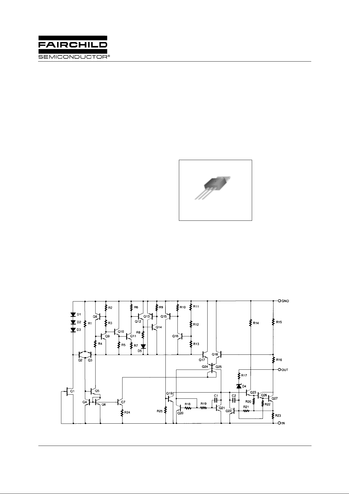
TO-220
1. GND 2. Input 3. Output
1
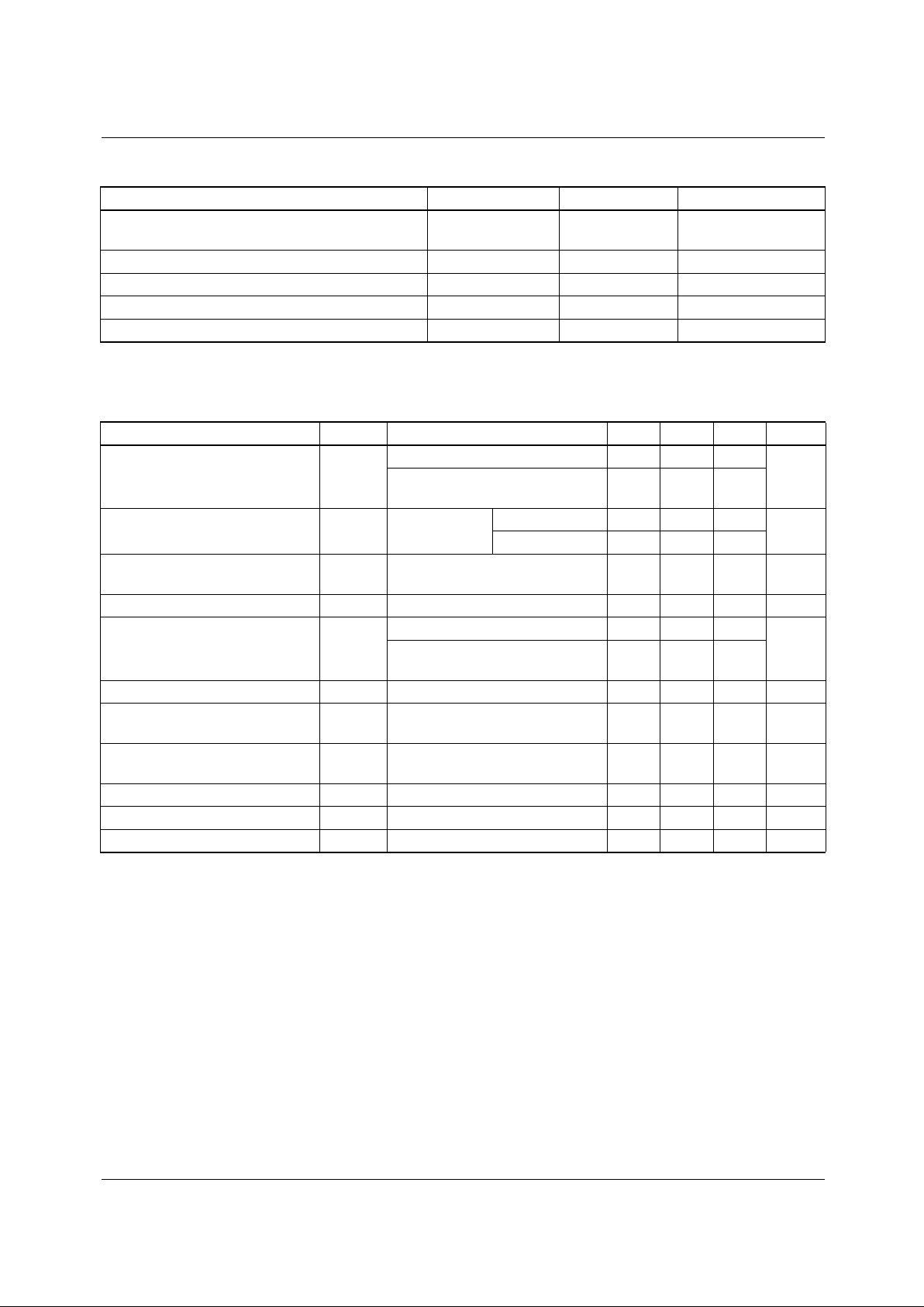
Schematic Diagram
MC79MXX
3-Terminal 0.5A Negative Voltage Regulator
Page 2
MC79MXX
2
Absolute Maximum Ratings
Electrical Characteristics (MC79M05)
(Refer to test circuit, 0
°C ≤TJ ≤ +125
°C, l
O
=350mA, VI = -10V,unless otherwise specified, CI =0.33µF,CO=0.1µF)
Note:
1. Load and line regulation are specified at constant junction temperature. Change in VO due to heating effects must be take n
into account separately. Pulse testing with low duty is used.
Parameter Symbol Value Unit
Input Voltage(for V
O
= -5V to -18V)
(for V
O
= -24V)
V
I
V
I
-35
-40
V
V
Thermal Resistance Junction-Cases R
θJC
5 °C /W
Thermal Resistance Junction-Air R
θJA
65 °C /W
Operating Temperature Range T
OPR
0 ~ +125 °C
Storage Temperature Range T
STG
-65 ~ +125 °C
Parameter Symbol Conditions Min. Typ. Max. Unit
Output Voltage V
O
TJ= +25 °C -4.8 -5 -5.2
V
I
O
= 5mA to 350mA
V
I
= -7V to -25V
-4.75 -5 -5.25
Line Regulation (Note1) ∆V
O
TJ =+25°C
V
I
= -7V to -25V - 7.0 50
mV
V
I
= -8V to -25V - 2.0 30
Load Regulation (Note1) ∆V
O
IO = 5mA to 500mA
T
J
= +25 °C
- 30 100 mV
Quiescent Current I
Q
TJ= +25 °C-3.06.0mA
Quiescent Current Change ∆I
Q
IO = 5mA to 350mA - - 0.4
mA
I
O
= 200mA
V
I
= -8V to -25V
--0.4
Output Voltage Drift ∆Vo/∆TI
O
= 5mA - -0.2 - mV/ °C
Output Noise Voltage V
N
f = 10Hz, 100KHz
T
A
= +25 °C
-40-µV
Ripple Rejection RR
f = 120Hz
V
J
= -8 to -18V
54 60 - dB
Dropout Voltage V
D
TJ =+25 °C, IO = 500mA - 1.1 - V
Short Circuit Current I
SC
TJ= +25 °C, VI = -35V - 140 - mA
Peak Current I
PK
TJ= +25 °C - 650 - mA
Page 3

MC79MXX
3
Electrical Characteristics (MC79M06)
(Refer to test circuit, 0
°C ≤TJ ≤ +125 °C, l
O
=350mA, VI = -11V,unless otherwise specified)
Note:
1. Load and line regulation are specified at constant junction temperature. Change in VO due to heating effects must be take n
into account separately. Pulse testing with low duty is used.
Parameter Symbol Conditions Min. Typ. Max. Unit
Output Voltage V
O
TJ= +25 °C - 5.75 - 6.0 - 6.25
V
I
O
= 5mA to 350mA
V
I
= -8.0V to -25V - 5.7 - 6.0 - 6.3
Line Regulation (Note1) ∆V
O
TJ =+25°C
V
I
= -8V to -25V - 7.0 60
mV
V
I
= -9V to -19V - 2.0 40
Load Regulation (Note1) ∆V
O
TJ= +25 °CIO = 5.0mA to 500mA - 30 120 mV
Quiescent Current I
Q
TJ= +25 °C-36mA
Quiescent Current Change ∆I
Q
IO = 5mA to 350mA - - 0.4
mA
V
I
= -8V to -25V - - 0.4
Output Voltage Drift ∆V
O
/∆TIO = 5mA - 0.4 - mV/ °C
Output Noise Voltage V
N
f = 10Hz to 100KHz,TA = +25 °C-50-µV
Ripple Rejection RR f = 120Hz,V
I
= -9V to -19V 54 60 - dB
Dropout Voltage V
D
IO = 500mA, TJ = +25 °C-1.1-V
Short Circuit Current I
SC
VI = -35V, TJ = +25 °C - 140 - mA
Peak Current I
PK
TJ= +25 °C - 650 - mA
Page 4

MC79MXX
4
Electrical Characteristics (MC79M08)
(Refer to test circuit, 0
°C ≤TJ ≤ +125 °C, l
O
=350mA, VI = -14V,unless otherwise specified)
Note:
1. Load and line regulation are specified at constant junction temperature. Change in VO due to heating effects must be take n
into account separately. Pulse testing with low duty is used.
Parameter Symbol Conditions Min. Typ. Max. Unit
Output Voltage V
O
TJ= +25 °C - 7.7 - 8.0 - 8.3
V
I
O
= 5mA to 350mA
V
I
= -10.5V to -25V - 7.6 - 8.0 - 8.4
Line Regulation (Note1) ∆V
O
TJ =+25°C
V
I
= -10.5V to -25V - 7.0 80
mV
V
I
= -11V to -21V - 2.0 50
Load Regulation (Note1) ∆V
O
TJ= +25 °CIO = 5.0mA to 500mA - 30 160 mV
Quiescent Current I
Q
TJ= +25 °C-36mA
Quiescent Current Change ∆I
Q
IO = 5mA to 350mA - - 0.4
mA
V
I
= -8V to -25V - - 0.4
Output Voltage Drift ∆V
O
/∆TIO = 5mA - -0.6 - mV/ °C
Output Noise Voltage V
N
f = 10Hz to 100KHz,TA = +25 °C-60-µV
Ripple Rejection RR f = 120Hz,V
I
= -9V to -19V 54 59 - dB
Dropout Voltage V
D
IO = 500mA, TJ = +25 °C-1.1-V
Short Circuit Current I
SC
VI = -35V, TJ = +25 °C - 140 - mA
Peak Current I
PK
TJ = +25 °C - 650 - mA
Page 5
MC79MXX
5
Electrical Characteristics (MC79M12)
(Refer to test circuit, 0
°C ≤TJ ≤ +125 °C, l
O
=350mA, VI = -19V,unless otherwise specified)
Note:
1. Load and line regulation are specified at constant junction temperature. Change in VO due to heating effects must be take n
into account separately. Pulse testing with low duty is used.
Parameter Symbol Conditions Min. Typ. Max. Unit
Output Voltage V
O
TJ= +25 °C -11.5 -12 -12.5
V
I
O
= 5mA to 350mA
V
I
= -14.5V to -30V -11.4 -12 -12.6
Line Regulation (Note1) ∆V
O
TJ =+25°C
V
I
= -14.5V to -30V - 8.0 80
mV
V
I
= -15V to -25V - 3.0 50
Load Regulation (Note1) ∆V
O
TJ= +25 °CIO = 5.0mA to 500mA - 30 240 mV
Quiescent Current I
Q
TJ= +25 °C-36mA
Quiescent Current Change ∆I
Q
IO = 5mA to 350mA - - 0.4
mA
V
I
= -14.5V to -30V - - 0.4
Output Voltage Drift ∆V
O
/∆TIO = 5mA - -0.8 - mV/ °C
Output Noise Voltage V
N
f = 10Hz to 100KHz,TA =+25 °C-75-µV
Ripple Rejection RR f = 120Hz,V
I
= -15V to -25V 54 60 - dB
Dropout Voltage V
D
IO = 500mA, TJ = +25 °C-1.1-V
Short Circuit Current I
SC
VI = -35V, TJ = +25 °C - 140 - mA
Peak Current I
PK
TJ= +25 °C - 650 - mA
Page 6

MC79MXX
6
Electrical Characteristics (MC79M15)
(Refer to test circuit, 0
°C ≤TJ ≤ +125 °C, l
O
=350mA, VI = -23V,unless otherwise specified)
Note:
1. Load and line regulation are specified at constant junction temperature. Change in VO due to heating effects must be take n
into account separately. Pulse testing with low duty is used.
Parameter Symbol Conditions Min. Typ. Max. Unit
Output Voltage V
O
TJ= +25 °C - 14.4 - 15 - 15.6
V
I
O
= 5mA to 350mA
V
I
= -17.5V to -30V
-14.25 - 15 -15.75
Line Regulation (Note1) ∆V
O
TJ =+25°C
V
I
= -17.5V to -30V - 9.0 80
mV
V
I
= -18V to -28V - 5.0 50
Load Regulation (Note1) ∆V
O
TJ= +25 °CIO = 5.0mA to 500mA - 30 240 mV
Quiescent Current I
Q
TJ= +25 °C-36mA
Quiescent Current Change ∆I
Q
IO = 5mA to 350mA - - 0.4
mA
V
I
= -17.5V to -28V - - 0.4
Output Voltage Drift ∆V
O
/∆TIO = 5mA - -1.0 - mV/ °C
Output Noise Voltage V
N
f = 10Hz to 100KHz,TA = +25 °C-90-µV
Ripple Rejection RR f = 120Hz,V
I
= -18.5V to -28.5V 54 59 - dB
Dropout Voltage V
D
IO = 500mA, TJ = +25 °C-1.1-V
Short Circuit Current I
SC
VI = -35V, TJ = +25 °C - 140 - mA
Peak Current I
PK
TJ= +25 °C - 650 - mA
Page 7

MC79MXX
7
Electrical Characteristics (MC79M18)
(Refer to test circuit, 0
°C ≤TJ ≤ +125 °C, l
O
=350mA, VI = -27V,unless otherwise specified)
Note;
1. Load and line regulation are specified at constant junction temperature. Change in VO due to heating effects must be take n
into account separately. Pulse testing with low duty is used.
Parameter Symbol Conditions Min. Typ. Max. Unit
Output Voltage V
O
TJ= +25 °C - 17.3 - 18 - 18.7
V
I
O
= 5mA to 350mA
V
I
= -21V to -33V
- 17.1 - 18 - 18.9
Line Regulation (Note1) ∆V
O
TJ =+25°C
V
I
= -21V to -33V - 9.0 80
mV
V
I
= -24V to -30V - 5.0 80
Load Regulation (Note1) ∆V
O
TJ= +25 °CIO = 5.0mA to 500mA - 30 360 mV
Quiescent Current I
Q
TJ= +25 °C-36mA
Quiescent Current Change ∆I
Q
IO = 5mA to 350mA - - 0.4
mA
V
I
= -21V to -33V - - 0.4
Output Voltage Drift ∆V
O
/∆TIO = 5mA - -1.0 - mV/ °C
Output Noise Voltage V
N
f = 10Hz to 100KHz,TA = +25 °C-110-µV
Ripple Rejection RR f = 120Hz,V
I
= -22V to -32V 54 59 - dB
Dropout Voltage V
D
IO = 500mA, TJ = +25 °C-1.1-V
Short Circuit Current I
SC
VI = -35V, TJ = +25 °C - 140 - mA
Peak Current I
PK
TJ= +25 °C - 650 - mA
Page 8

MC79MXX
8
Electrical Characteristics (MC79M24)
(Refer to test circuit, 0
°C ≤TJ ≤ +125 °C, l
O
=350mA, VI = -33V,unless otherwise specified)
Note:
1. Load and line regulation are specified at constant junction temperature. Change in VO due to heating effects must be take n
into account separately. Pulse testing with low duty is used.
Parameter Symbol Conditions Min. Typ. Max. Unit
Output Voltage V
O
TJ= +25 °C - 23 - 24 - 25
V
I
O
= 5mA to 350mA
V
I
= -27V to -38V
- 22.8 - 24 - 25.2
Line Regulation (Note1) ∆V
O
TJ =+25°C
V
I
= -27V to -38V - 9.0 80
mV
V
I
= -30V to -36V - 5.0 70
Load Regulation (Note1) ∆V
O
TJ= +25 °CIO = 5.0mA to 500mA - 30 300 mV
Quiescent Current I
Q
TJ= +25 °C-36mA
Quiescent Current Change ∆I
Q
IO = 5mA to 350mA - - 0.4
mA
V
I
= -27V to -38V - - 0.4
Output Voltage Drift ∆V
O
/∆TIO = 5mA - -1.0 - mV/ °C
Output Noise Voltage V
N
f = 10Hz to 100KHz,TA = +25 °C - 180 - µV
Ripple Rejection RR f = 120Hz,V
I
= -28V to -38V 54 58 - dB
Dropout Voltage V
D
IO = 500mA, TJ = +25 °C-1.1-V
Short Circuit Current I
SC
VI = -35V, TJ = +25 °C - 140 - mA
Peak Current I
PK
TJ= +25 °C - 650 - mA
Page 9

MC79MXX
9
Typical Applications
Figure 1. Fixed Output Regulator
Figure 2. Variable Output
Notes:
1. Required for stability. For value given, capacitor must be solid tantalum. 25µF aluminum electrolytic may be substituted.
2. C
2
improves tr ansient response and ripple r ejection. Do not increase beyond 50µF.
MC79MXX
MC79MXX
Page 10

MC79MXX
10
Mechanical Dimensions
Package
Dimensions in millimeters
4.50
±0.20
9.90
±0.20
1.52
±0.10
0.80
±0.10
2.40
±0.20
10.00
±0.20
1.27
±0.10
ø3.60
±0.10
(8.70)
2.80
±0.10
15.90
±0.20
10.08
±0.30
18.95MAX.
(1.70)
(3.70)(3.00)
(1.46)
(1.00)
(45°)
9.20
±0.20
13.08
±0.20
1.30
±0.10
1.30
+0.10
–0.05
0.50
+0.10
–0.05
2.54TYP
[2.54
±0.20
]
2.54TYP
[2.54
±0.20
]
TO-220
Page 11

MC79MXX
11
Mechanical Dimensions
(Continued)
Package
Dimensions in millimeters
6.60
±0.20
2.30
±0.10
0.50
±0.10
5.34
±0.30
0.70
±0.20
0.60
±0.20
0.80
±0.20
9.50
±0.30
6.10
±0.20
2.70
±0.20
9.50
±0.30
6.10
±0.20
2.70
±0.20
MIN0.55
0.76
±0.10
0.50
±0.10
1.02
±0.20
2.30
±0.20
6.60
±0.20
0.76
±0.10
(5.34)
(1.50)
(2XR0.25)
(5.04)
0.89
±0.10
(0.10) (3.05)
(1.00)
(0.90)
(0.70)
0.91
±0.10
2.30TYP
[2.30±0.20]
2.30TYP
[2.30±0.20]
MAX0.96
(4.34)(0.50) (0.50)
D-PAK
Page 12

MC79MXX
12
Ordering Information
Product Number Package Operating Temperature
MC79M05CT
TO-220 0 ~ + 125°C
MC79M06CT
MC79M08CT
MC79M12CT
MC79M15CT
MC79M18CT
MC79M24CT
Page 13

MC79MXX
13
Page 14

MC79MXX
6/11/01 0.0m 001
Stock#DSxxxxxxxx
2001 Fairchild Semiconductor Corporation
LIFE SUPPORT POL I CY
FAIRCHILD’S PRODUCTS ARE NOT AUTHORIZED FOR USE AS CRITICAL COMPONENTS IN LIFE SUPPORT DEVICES
OR SYSTEMS WITHOUT THE EXPRESS WRITTEN APPROVAL OF THE PRESIDENT OF FAIRCHILD SEMICONDUCTOR
CORPORATION. As used herein :
1. Life support devices or systems are devices or systems
which, (a) are intended for surgical implant into the body,
or (b) support or sustain life, and (c) whose failure to
perform when properly used in accordance with
instructions for use provided in the labeling, can be
reasonably expected to result in a significant injury of the
user.
2. A critical component in any component of a life support
device or sys tem whose failure to perform can be
reasonably expec ted to cause the failur e of the life support
device or system, or to affect its safety or effec tiveness.
www.fairchildsemi.com
DISCLAIMER
FAIRCHILD SEMICONDUCTOR RESERVES THE RIGHT TO MAKE CHANGES WITHOUT FURTHER NOTICE TO ANY
PRODUCTS HEREI N TO IMPROVE RELIABILITY, FUNCTION OR DES IGN. FAIRCHILD DOES NOT ASSUME ANY
LIABILITY ARISING OUT OF THE APPLICATION OR USE OF ANY PRODUCT OR CIRCUIT DESCRIBED HEREIN; NEITHER
DOES IT CONVEY ANY LICENSE UNDER ITS PATENT RIGHTS, NOR THE RI GHTS OF OTHERS.
 Loading...