

Page 1
www.fairchildsemi.com
Features
• Output current up to 100mA
• No external components
• Internal thermal over load protection
• Internal short circuit current limiting
• Output Voltage Offered in ± 5% Tolerance
• Output Voltage of -5V, -8V, -12V, -15V, -18V
and -24V
Description
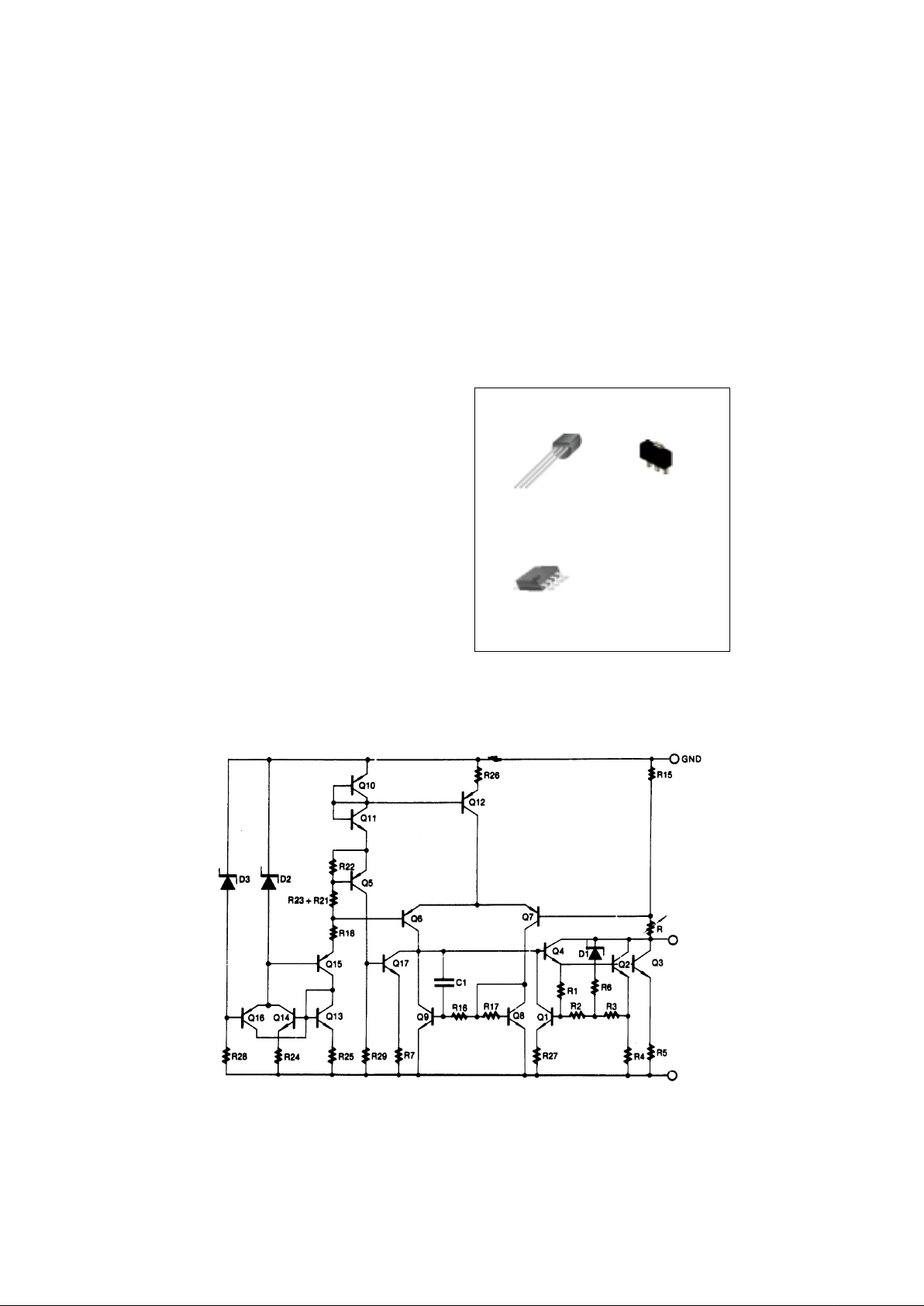
These regulators employ internal current limiting and thermal shutdown, making them essentially indestructible.
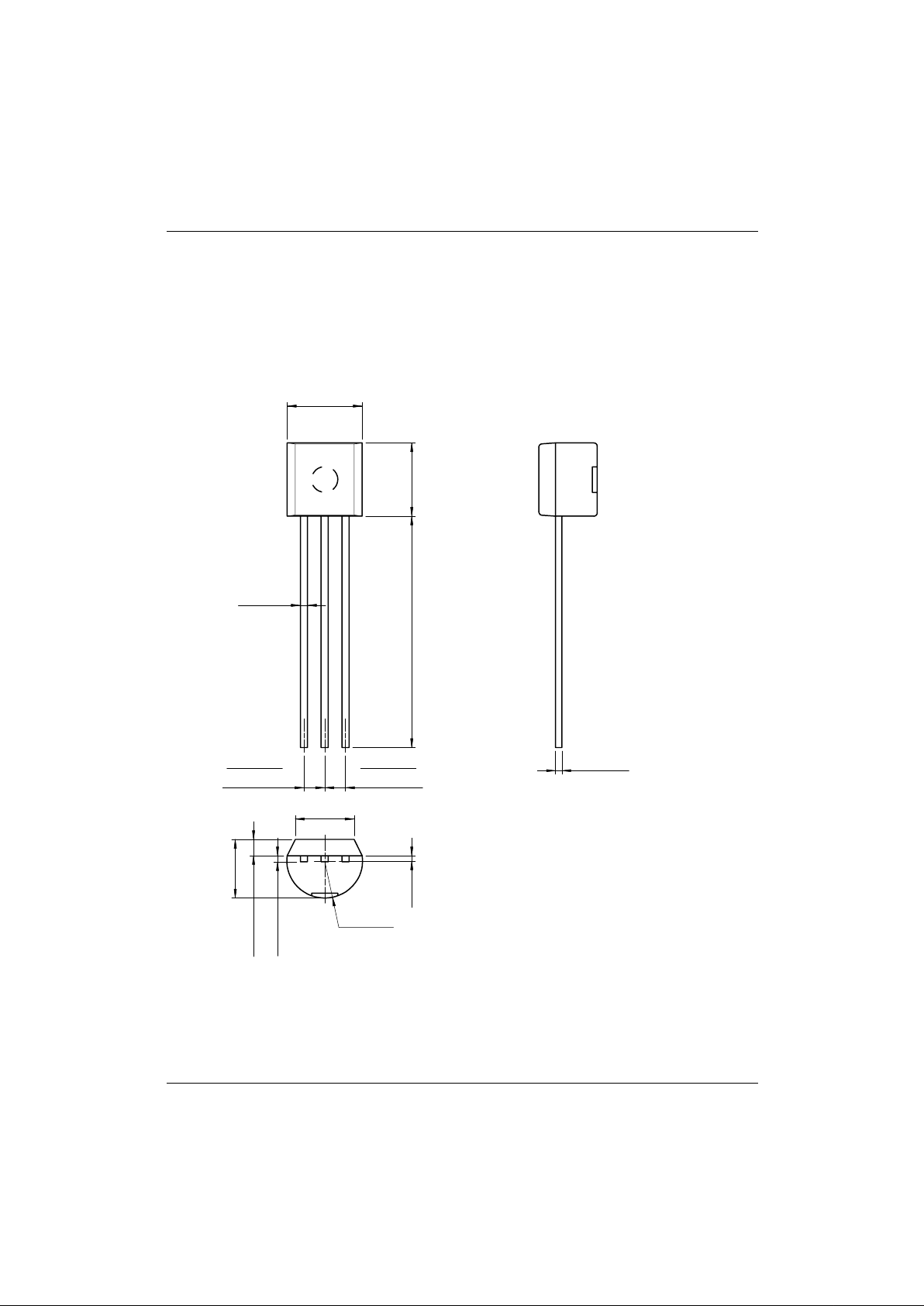
TO-92
1.GND 2.Input 3.Output
1
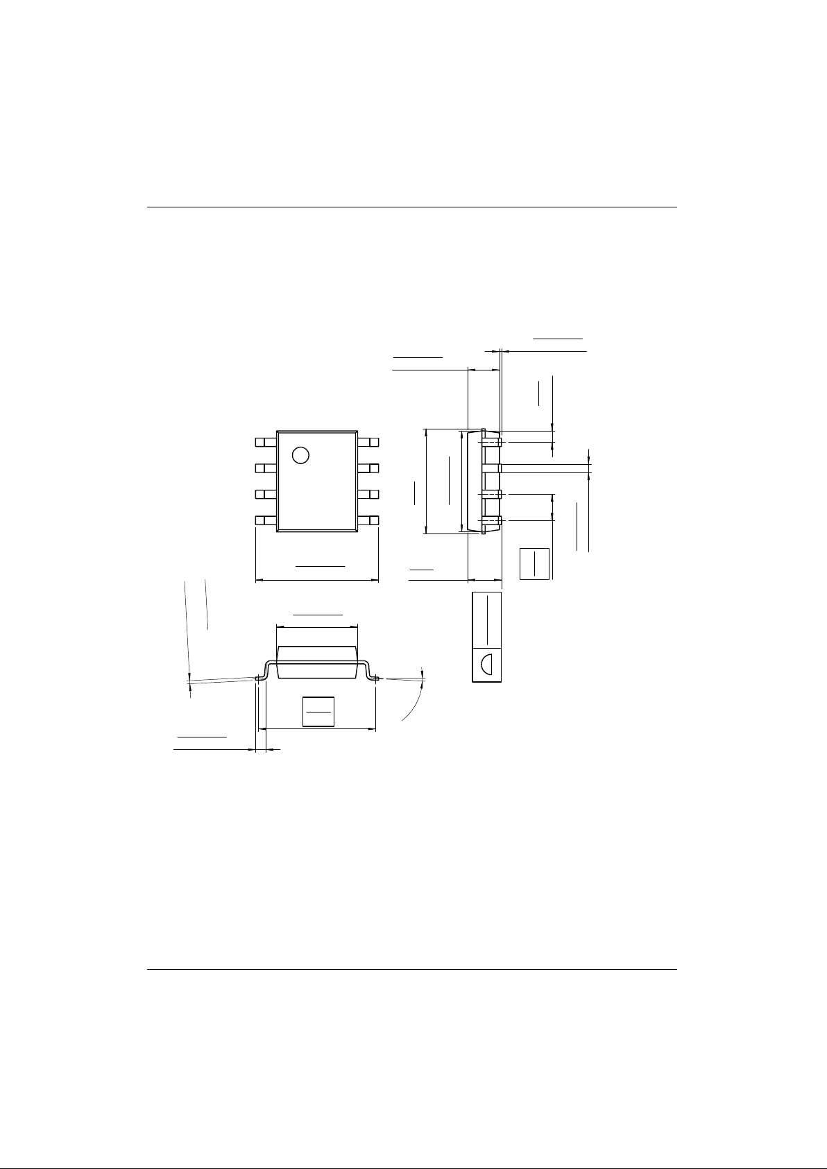
8-SOP
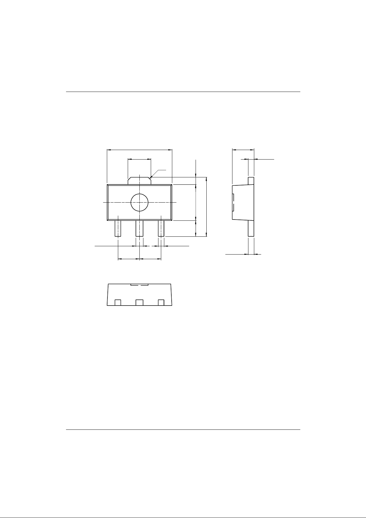
SOT-89
1
1
1. Output 2.3.6.7. GND 4.5. NC 8. Input
Internal Block Diagram
Output
Input
KA79LXXA
3-Terminal 0.1A Negative Voltage Regulator
Page 2
KA79LXXA
2
Absolute Maximum Ratings
Electrical Characteristics(KA 79L05A)
(VI = -10V, IO = 40mA, CI = 0.33µF, CO = 0.1µF, 0°C ≤T
J
≤ +125°C, unless otherwise specified)
Note
1. Load and line regulation are specified at constant junction temperature. Change in V
O
due to heating effects must be taken
into account separately. Pulse testing with low duty is used.
Parameter Symbol Value Unit
Input Voltage (for V
o
= -5V to -8V)
(for V
o
= -12V to -18V)
(for V
o
= -24V)
V
I
-30
-35
-40
V
Operating Temperature Range T
OPR
0 ~ +125 °C
Storage Temperature Range T
STG
-65 ~ +150 °C
Parameter Symbol Conditions Min. Typ. Max. Unit
Output Voltage V
O
TJ = +25
°C - 4.8 - 5.0 - 5.2 V
Line Regulation (Note1)
∆V
OTJ
=+25
°C
-7.0V ≥ V
I
≥-20V - 15 150 mV
-8V ≥ V
I
≥-20V - - 100 mV
Load Regulation (Note1) ∆V
OTJ
=+25
°C
1.0mA ≤ I
O
≤
100mA
-2060mV
1.0mA ≤ I
O
≤ 40mA - 10 30 mV
Output Voltage V
O
-7.0V≥ V
I
≥ -20V, 1.0mA ≤ IO ≤ 40mA - 4.75 - - 5.25 V
V
I
= -10V, 1.0mA≤ I
O
≤70mA - 4.75 - - 5.25 V
Quiescent Current I
Q
TJ =+ 25
°C-2.05.5
mA
T
J
= +125
°C--6.0
Quiescent Current
Change
with line ∆I
Q
-8V≥ V
I
≥-20V - - 1.5 mA
with load ∆I
Q
1.0mA≤ I
O
≤40mA - - 0.1 mA
Output Noise Voltage V
N
TA = +25°C,10Hz≤f≤100KHz - 30 - µV
Ripple Rejection RR
f = 120Hz, -8V≥V
I
≥-18V
T
J
= +25°C
41 60 - dB
Dropout Voltage V
D
TJ = +25°C-1.7-V
Page 3
KA79LXXA
3
Electrical Characteristic s (K A 79L08A)
(VI = -14V, IO = 40mA, CI = 0.33µF, CO = 0.1µF, 0°C ≤T
J
≤ +125°C, unless otherwise specified)
Note
1. Load and line regu lati on a re sp eci fied at c ons tant junc tion tem per ature . Ch ange in V
O
due to heating effects must be taken
into account separately. Pulse testing with low duty is used.
Parameter Symbol Conditions Min. Typ. Max. Unit
Output Voltage V
O
TJ = +25
°C - 7.7 - 8.0 - 8.3 V
Line Regulation (Note1)
∆V
OTJ
=+25
°C
-10.3V ≥ V
I
≥ -23V - - 175 mV
-12V ≥ VI ≥ -23V - - 125 mV
Load Regulation (Note1) ∆V
OTJ
=+25
°C
1.0mA ≤ I
o
≤ 100mA - - 80 mV
1.0mA ≤ I
o
≤ 40mA - - 40 mV
Output Voltage V
O
-10.3V ≥ V
I
≥ -23V, 1.0mA ≤ Io ≤ 40mA - 7.6 - - 8.4
V
V
I
= -14V, 1.0mA ≤ I
o
≤ 70mA - 7.6 - - 8.4
Quiescent Current I
Q
Tj =+ 25
°C--6.0
mA
T
j
= +125
°C--5.5
Quiescent Current
Change
with line
∆I
Q
-11.7V ≥ V
I
≥ -23V - - 1.5 mA
with load 1.0mA ≤ I
o
≤ 40mA - - 0.1 mA
Output Noise Voltage V
N
Tj = +25°C,10Hz ≤ f ≤ 100KHz - 50 - µV
Ripple Rejection RR
f = 120Hz, -11V ≥ V
I
≥ -21V
T
j
= +25°C
39 55 - dB
Dropout Voltage V
D
Tj = +25°C-1.7-V
Page 4
KA79LXXA
4
Electrical Characteristics(KA 79L12A)
(VI = -19V, IO = 40mA, CI = 0.33µF, CO = 0.1µF, 0°C ≤T
J
≤ +125°C, unless otherwise specified)
Note
1. Load and line regulation are specified at constant junction temperature. Change in V
O
due to heating effects must be taken
into account separately. Pulse testing with low duty is used.
Parameter Symbol Conditions Min. Typ. Max. Unit
Output Voltage V
O
TJ = +25
°C -11.5 -12.0 -12.5 V
Line Regulation (Note1)
∆V
OTJ
= +25
°C
-14.5V ≥V
I
≥-27V - - 250 mV
-16V≥VI ≥-27V - - 200 mV
Load Regulation (Note1) ∆V
OTJ
= +25
°C
1.0mA≤ I
O
≤100mA - - 100 mV
1.0mA≤ I
O
≤40mA - - 50 mV
Output Voltage V
O
-14.5V >V
I
> -27V, 1.0mA ≤IO ≤ 40mA -11.4 - -12.6 V
V
I
= -19V, 1.0mA ≤ I
O
≤ 70mA -11.4 - -12.6 V
Quiescent Current I
Q
TJ = +25
°C--6.0
mA
T
J
= +125
°C--6.5
Quiescent Current
Change
with line ∆I
Q
-16V ≥ V
I
≥ -27V - - 1.5 mA
with load ∆I
Q
1.0mA ≤ I
O
≤ 40mA - - 0.1 mA
Output Noise Voltage V
N
TA = +25°C,10Hz ≤ f ≤ 100KHz - 80 - µV
Ripple Rejection RR
f = 120Hz, -15V ≥ V
I
≥ -25V
T
J
= +25°C
37 42 - dB
Dropout Voltage V
D
TJ = +25°C-1.7-V
Page 5
KA79LXXA
5
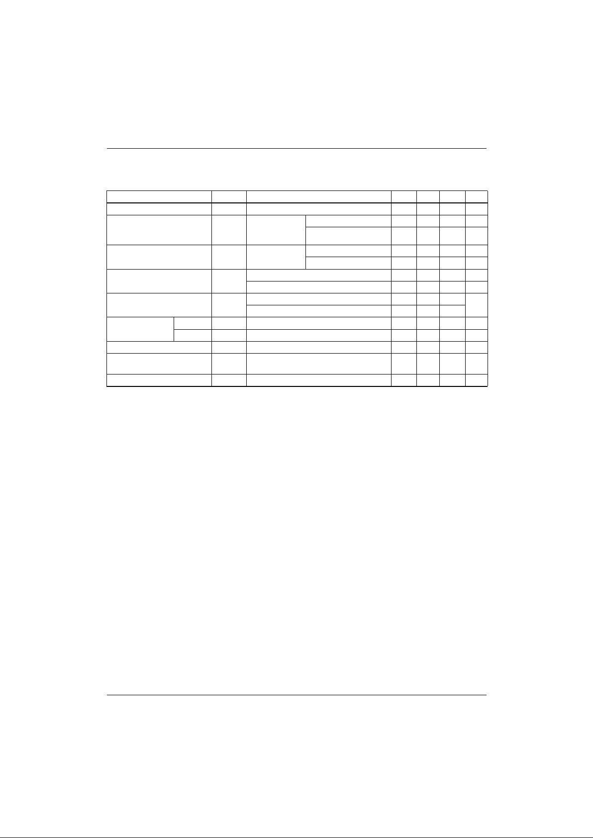
Electrical Characteristics(KA 79L15A)
(VI = -23V, IO = 40mA, CI = 0.33µF, CO = 0.1µF, 0°C ≤T
J
≤ +125°C, unless otherwise specified)
Note
1. Load and line regu lati on a re sp eci fied at c ons tant junc tion tem per ature . Ch ange in V
O
due to heating effects must be taken
into account separately. Pulse testing with low duty is used.
Parameter Symbol Conditions Min. Typ. Max. Unit
Output Voltage V
O
TJ = +25
°C -14.4 -15.0 -15.6 V
Line Regulation (Note1)
∆V
OTJ
= +25
°C
-17.5V ≥ V
I
≥ -30V - - 300 mV
-20V ≥ VI ≥ -30V - - 250 mV
Load Regulation (Note1) ∆V
OTJ
= +25
°C
1.0mA ≤ I
O
≤ 100mA - - 150 mV
1.0mA ≤ I
O
≤ 40mA - - 75 mV
Output Voltage V
O
-17.5V ≥ V
I
≥ -30V, 1.0mA ≤ IO ≤ 40mA -14.25 - -15.75 V
V
I
= -23V, 1.0mA ≤ I
O
≤ 70mA -14.25 - -15.75 V
Quiescent Current I
Q
TJ = +25°C--6.0
mA
T
J
= +125°C--6.5
Quiescent Current
Change
with line ∆I
Q
-20V ≥ V
I
≥ -30V - - 1.5 mA
with load ∆I
Q
1.0mA ≤ I
O
≤ 40mA - - 0.1 mA
Output Noise Voltage V
N
TA = +25°C,10Hz ≤ f ≤ 100KHz - 90 - µV
Ripple Rejection RR
f = 120Hz, -18.5V ≥ V
I
≥ -28.5V
T
J
= +25°C
34 39 - dB
Dropout Voltage V
D
TJ = +25°C-1.7-V
Page 6
KA79LXXA
6
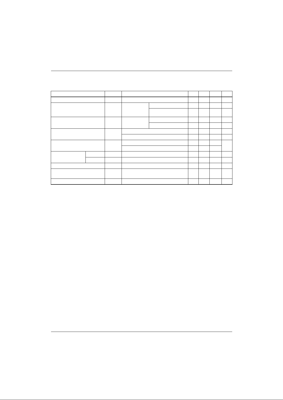
Electrical Characteristics(KA 79L18A)
(VI = -27V, IO = 40mA, CI = 0.33µF, CO = 0.1µF, 0°C ≤T
J
≤ +125°C, unless otherwise specified)
Note
1. Load and line regulation are specified at constant junction temperature. Change in V
O
due to heating effects must be taken
into account separately. Pulse testing with low duty is used.
Parameter Symbol Conditions Min. Typ. Max. Unit
Output Voltage V
O
TJ = +25
°C -17.3 -18.0 -18.7 V
Line Regulation (Note1)
∆V
OTJ
= +25
°C
-20.7V ≥ V
I
≥ -33V - - 325 mV
-21V ≥ VI ≥ -33V - - 275 mV
Load Regulation (Note1) ∆V
OTJ
= +25
°C
1.0mA ≤ I
O
≤ 100mA - - 170 mV
1.0mA ≤ I
O
≤ 40mA - - 85 mV
Output Voltage V
O
-20.7V > V
I
> -33V, 1.0mA ≤ IO ≤ 40mA -17.1 - -18.9 V
V
I
= -27V, 1.0mA ≤ I
O
≤ 70mA -17.1 - -18.9 V
Quiescent Current I
Q
TJ = +25°C--6.5
mA
T
J
= +125°C--6.0
Quiescent Current
Change
with line ∆I
Q
-21V ≥ V
I
≥ -33V - - 1.5 mA
with load ∆I
Q
1.0mA ≤ I
O
≤ 40mA - - 0.1 mA
Output Noise Voltage V
N
TA =+25°C,10Hz ≤ f ≤ 100KHz - 150 - µV
Ripple Rejection RR
f = 120Hz, -23V ≥ V
I
≥ -33V
T
J
= +25°C
33 48 - dB
Dropout Voltage V
D
TJ = +25°C-1.7-V
Page 7
KA79LXXA
7
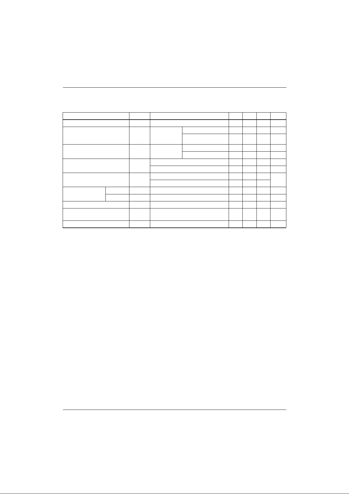
Electrical Characteristics(KA 79L24A)
(VI = -33V, IO = 40mA, CI = 0.33µF, CO = 0.1µF, 0°C ≤T
J
≤ +125°C, unless otherwise specified)
Note
1. Load and line regu lati on a re sp eci fied at c ons tant junc tion tem per ature . Ch ange in V
O
due to heating effects must be taken
into account separately. Pulse testing with low duty is used.
Parameter Symbol Conditions Min. Typ. Max. Unit
Output Voltage V
O
TJ = +25
°C -23 -24 -25 V
Line Regulation (Note1)
∆V
OTJ
= +25
°C
-27V ≥ V
I
≥ -38V - - 350 mV
-28V ≥ VI ≥ -38V - - 300 mV
Load Regulation (Note1) ∆V
OTJ
= +25
°C
1.0mA ≤ I
O
≤100mA - - 200 mV
1.0mA ≤ I
O
≤ 40mA - - 100 mV
Output Voltage V
O
-27V ≥ V
I
≥ -38V, 1.0mA ≤ IO ≤ 40mA -22.8 - -25.2 V
V
I
= -33V, 1.0mA ≤ I
O
≤ 70mA -22.8 - -25.2 V
Quiescent Current I
Q
TJ = +25°C--6.5
mA
T
J
= +125°C--6.0
Quiescent Current
Change
with line ∆I
Q
-28V ≥ V
I
≥ -38V - - 1.5 mA
with load ∆I
Q
1.0mA ≤ I
O
≤ 40mA - - 0.1 mA
Output Noise Voltage V
N
TA = +25°C,10Hz ≤ f ≤100KHz - 200 - µV
Ripple Rejection RR
f = 120Hz, -29V ≥ V
I
≥ -35V
T
J
= +25°C
31 47 - dB
Dropout Voltage V
D
TJ = +25°C-1.7-V
Page 8
KA79LXXA
8
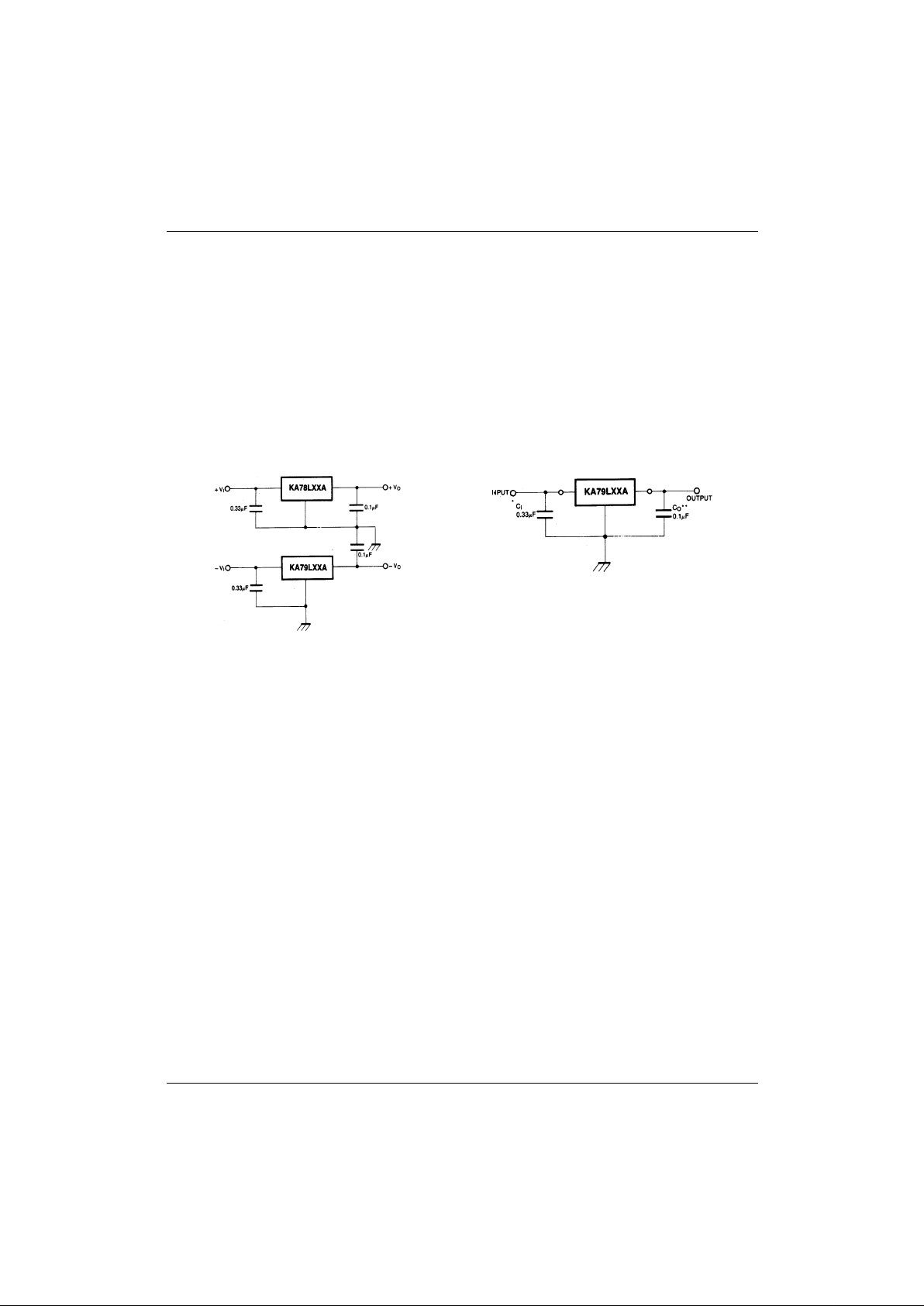
Typical Application
Design Considerations
The KA79LXXA Series of fixed voltage regulators are designed with Thermal Overload Protection that shuts down the circuit
when subjected to an excessive power overload condition. Internal Short Circuit Protection that limits the maximum current
the circuit will pass. In many low current applications, compensation capacitors are not required. However, it is recommended
that the regulator input be bypassed with a capacitor if the regulator is connected to the power supply filter with long wire
lengths, or if the output load capacitance is large. An input bypass capacitor should be selected to provide good high frequency
characteristics to insure stable operation under all load conditions. A 0.33µF or larger tantalum, mylar, or other capacitor having low internal impedance at high frequencies should be chosen. The bypass capacitor should be mounted with the shortest
possible leads directly across the regulator's input terminals. Normally good construction techniques should be used to minimize ground loops and lead resistance drops since the regulator has no external sense lead. Bypassing the output is also recommended.
A common ground is required between the input and the output voltages. The input voltage must remain typically 2.0V above
the output voltage even during the low point on the input ripple voltage.
* C1 is required if regulator is located an appreciable distance from power supply filter.
* C
O
improves stability and transient response.
Figure 1. Positive And Nega tive Regulator
Figure 2. Typical Application
I
Page 9
KA79LXXA
9
Mechanical Dimensions
Package
0.46
±0.10
1.27TYP
(R2.29)
3.86MAX
[1.27
±0.20
]
1.27TYP
[1.27
±0.20
]
3.60
±0.20
14.47
±0.40
1.02
±0.10
(0.25)
4.58
±0.20
4.58
+0.25
–0.15
0.38
+0.10
–0.05
0.38
+0.10
–0.05
TO-92
Page 10
KA79LXXA
10
Mechanical Dimensions
(Continued)
Package
4.92 ±0.20
0.194 ±0.008
0.41 ±0.10
0.016 ±0.004
1.27
0.050
5.72
0.225
1.55 ±0.20
0.061 ±0.008
0.1~0.25
0.004~0.001
6.00 ±0.30
0.236 ±0.012
3.95 ±0.20
0.156 ±0.008
0.50 ±0.20
0.020 ±0.008
5.13
0.202
MAX
#1
#4
#5
0~8°
#8
0.56
0.022
()
1.80
0.071
MAX0.10
MAX0.004
MAX
MIN
+
0.10
-0.05
0.15
+
0.004
-0.002
0.006
8-SOP
Page 11
KA79LXXA
11
Mechanical Dimensions
(Continued)
Package
SOT-89
0.40
±0.10
2.50
±0.20
(0.50)
(0.40)
4.10
±0.20
0.40
+0.10
–0.05
0.50
±0.10
1.65
±0.10
4.50
±0.20
1.50
±0.20
C0.2
1.50 TYP 1.50 TYP
(1.10)
Page 12
KA79LXXA
12
Ordering Information
Product Number Package Operating Temperature
KA79L05AZ
TO-92
0 ~ + 125°C
KA79L08AZ
KA79L12AZ
KA79L15AZ
KA79L18AZ
KA79L24AZ
KA79L05AD 8-SOP
KA79L05AM SOT-89
 Loading...