

Datasheet MC78PC28NTR, MC78PC30NTR, MC78PC33NTR, MC78PC50NTR, MC78PC18NTR Datasheet (MOTOROLA)
Page 1
MC78PC00 Series
Low Noise 150 mA
Low Drop Out (LDO)
Linear Voltage Regulator
The MC78PC00 are a series of CMOS linear voltage regulators with
high output voltage accuracy, low supply current, low dropout voltage,
and high Ripple Rejection. Each of these voltage regulators consists of
an internal voltage reference, an error amplifier, resistors, a current
limiting circuit and a chip enable circuit.
The dynamic Response to line and load is fast, which makes these
products ideally suited for use in hand–held communication
equipment.
The MC78PC00 series are housed in the SOT–23 5 lead package,
for maximum board space saving.
MC78PC00 Features:
• Ultra–Low Supply Current: typical 35
• Standby Mode: typical 0.1
m
A.
• Low Dropout Voltage: typical 0.2 V @ I
• High Ripple Rejection: typical 70 dB @ f = 1 kHz.
• Low Temperature–Drift Coefficient of Output Voltage:
typical ±100 ppm/°C.
• Excellent Line Regulation: typical 0.05%/V.
• High Accuracy Output Voltage: ±2.0%.
• Fast Dynamic Response to Line and Load.
• Small Package: SOT–23 5 leads.
• Built–in Chip Enable circuit (CE input pin).
• Identical Pinout to the LP2980/1/2.
MC78PC00 Applications:
• Power source for cellular phones (GSM, CDMA, TDMA), Cordless
Phones (PHS, DECT) and 2–way radios.
• Power source for domestic appliances such as cameras, VCRs and
camcorders.
• Power source for battery–powered equipment.
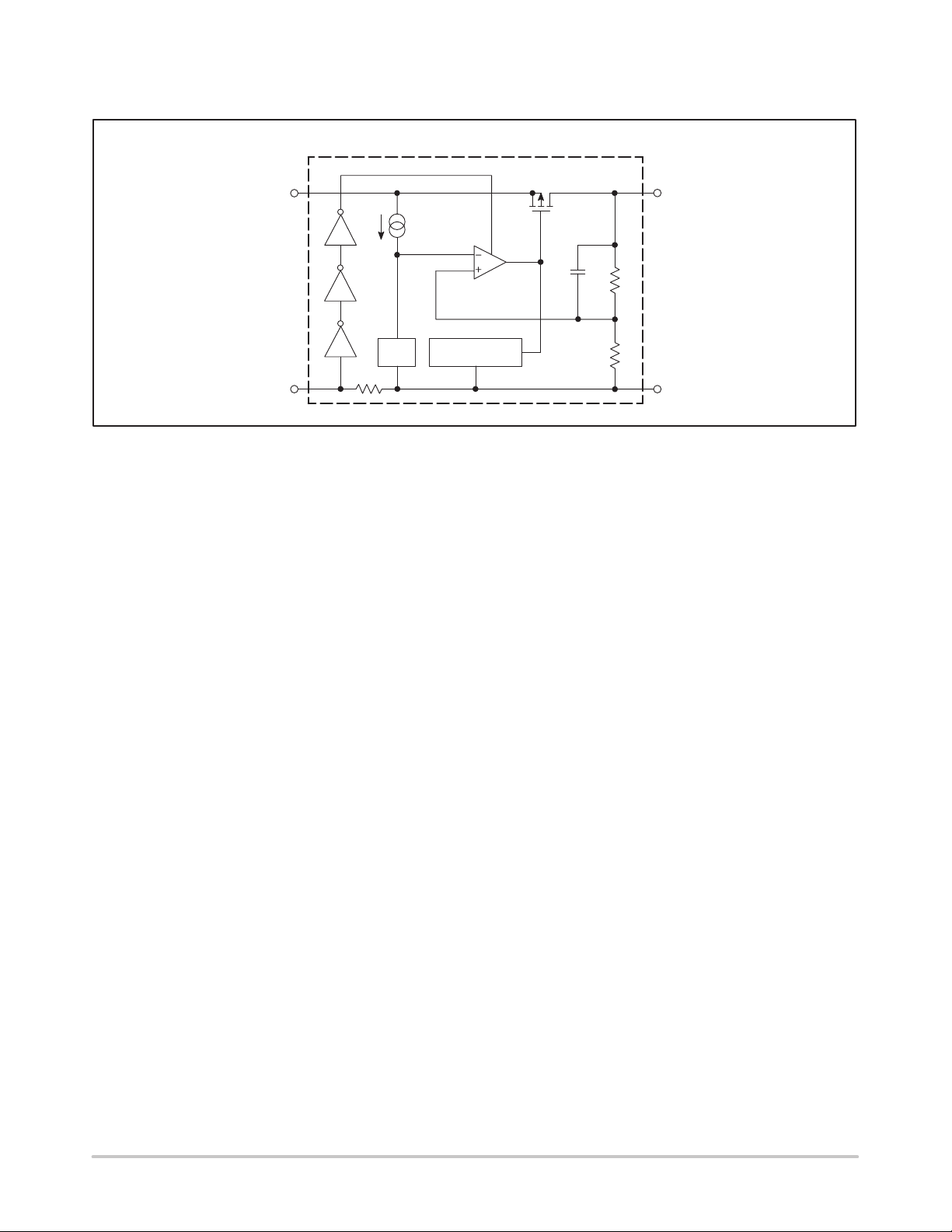
Block Diagram
1
V
IN
m
A in ON mode with no load.
= 100 mA.
OUT
MC78PCxx
5
V
OUT
http://onsemi.com
5
1
SOT–23–5
N SUFFIX
CASE 1212
PIN CONNECTIONS
V
IN
GND
CE
DEVICE MARKING
(4 digits are available for device marking)
Marking Voltage Version
1 2
3 4
Pin # Symbol Description
1
2
3
4
5
K8
F5 2.5 V
F8 2.8 V
G0
G3
J0
PINS DESCRIPTION
V
IN
GND
CE
N/C
V
OUT
ORDERING INFORMATION
1
15
2
2
3
3
4
(Top View)
V
OUT
N/C
4
1.8 V
3.0 V
3.3 V
5.0 V
Lot Number
Input Pin
Ground Pin
Chip Enable Pin
No Connection
Output Pin
ref
CURRENT LIMIT
V
3
CE
Semiconductor Components Industries, LLC, 1999
October, 1999 – Rev. 2
Device ShippingPackage
MC78PC18NTR
MC78PC25NTR
MC78PC28NTR
MC78PC30NTR
MC78PC33NTR
2
GND
1 Publication Order Number:
MC78PC50NTR
Other voltages are available. Consult your ON Semiconductor
representative.
SOT–23
5 Leads
3000 Units
Tape & Reel
MC78PC00/D
Page 2
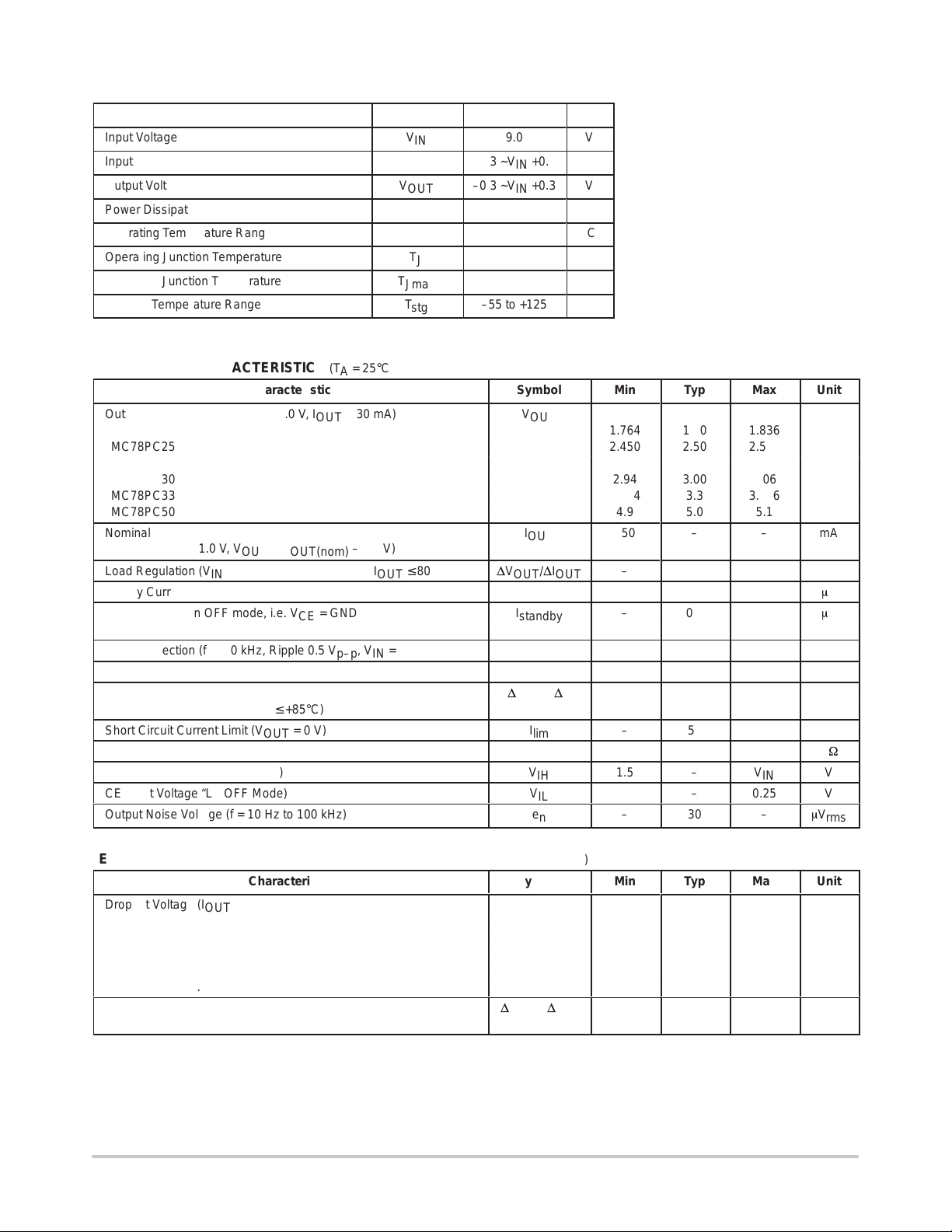
MAXIMUM RATINGS
Á
Á
Á
Á
Á
Á
Rating Symbol Value Unit
Input Voltage
Input Voltage
Output Voltage
Power Dissipation
Operating Temperature Range
Operating Junction Temperature
Maximum Junction Temperature
Storage Temperature Range
MC78PC00 Series
V
V
V
T
Jmax
T
IN
CE
OUT
P
D
T
A
T
J
stg
9.0
–0.3 ~VIN +0.3
–0.3 ~VIN +0.3
250
–40 to +85
+125
+150
–55 to +125
V
V
V
mW
°C
°C
°C
°C
ELECTRICAL CHARACTERISTICS (T
Characteristic
Output Voltage (VIN = V
OUT
+ 1.0 V, I
OUT
= 25°C)
A
= 30 mA)
Symbol Min Typ Max Unit
V
OUT
MC78PC18 1.764 1.80 1.836
MC78PC25 2.450 2.50 2.550
MC78PC28 2.744 2.80 2.856
MC78PC30 2.94 3.00 3.06
MC78PC33 3.234 3.3 3.366
MC78PC50 4.9 5.0 5.1
Nominal Output Current
ББББББББББББББББ
(VIN = V
Load Regulation (VIN = V
Supply Current in ON mode (VIN = V
OUT
+ 1.0 V, V
= V
OUT
OUT(nom)
+ 1.0 V, 1.0 mA ≤ I
OUT
OUT
– 0.1 V)
+ 1.0 V, I
≤ 80 mA)
OUT
= 0 mA) I
OUT
Supply Current in OFF mode, i.e. VCE = GND I
(VIN = V
Ripple Rejection (f = 1.0 kHz, Ripple 0.5 V
OUT
+ 1.0 V, I
OUT
= 0 mA)
p–p
, VIN = V
+ 1.0 V) RR – 70 – dB
OUT
Input Voltage V
Output Voltage Temperature Coefficient
(I
= 30 mA, –40°C ≤ TA ≤ +85°C)
OUT
Short Circuit Current Limit (V
= 0 V) I
OUT
CE Pull–down Resistance R
CE Input Voltage “H” (ON Mode) V
CE Input Voltage “L” (OFF Mode) V
Output Noise Voltage (f = 10 Hz to 100 kHz)
I
OUT
ÁÁÁ
D
V
/DI
OUT
SS
standby
IN
D
V
OUT
lim
PD
IH
IL
e
n
OUT
/DT
150
ÁÁ
–
–
ÁÁ
12
– 35 70
– 0.1 1.0
– – 8.0 V
– ±100 – ppm/°C
– 50 – mA
2.5 5.0 10
1.5 – V
0 – 0.25 V
–
30
–
ÁÁ
40
IN
–
mA
Á
mV
m
m
M
m
V
V
A
A
W
V
rms
ELECTRICAL CHARACTERISTICS by OUTPUT VOLTAGE V
Characteristic
Dropout Voltage (I
1.8 ≤ V
OUT
2.0 ≤ V
OUT
2.5 ≤ V
OUT
2.8 ≤ V
OUT
3.4 ≤ V
OUT
Line Regulation
(V
+ 0.5 V ≤ VIN ≤ 8.0 V, I
OUT
≤ 1.9 – 0.60 1.40
≤ 2.4 – 0.35 0.70
≤ 2.7 – 0.24 0.35
≤ 3.3 – 0.20 0.30
≤ 6.0 – 0.17 0.26
OUT
= 100 mA)
OUT
= 30 mA) – 0.05 0.20
(T
OUT
Symbol Min Typ Max Unit
D
V
OUT
http://onsemi.com
2
A
V
DIF
= 25°C)
/DV
IN
V
%/V
Page 3
MC78PC00 Series
OPERATION
MC78PC00
R1
R2
5
V
OUT
2
GND
1
V
IN
3
CE
In the MC78PC00, the output voltage V
ERROR AMP.
V
OUT
CURRENT LIMIT
ref
is detected by R1, R2. The detected output voltage is then compared to the
internal voltage reference by the error amplifier. Both a current limiting circuit for short circuit protection, and a chip ena ble
circuit are included.
http://onsemi.com
3
Page 4
MC78PC00 Series
TEST CIRCUITS
Figure 1. Standard T est Circuits
3
CE
IN
0.1 mF
1
V
IN
MC78PCxx
Series
2 GND
Figure 3. Ripple Rejection, Line
Transient Response Test Circuit
3
CE
IN
P.G.
1
V
IN
MC78PCxx
Series
2 GND
5
V
5
V
OUT
OUT
I
OUT
2.2 mF
I
OUT
10 mF
OUT
OUT
IN
Figure 2. Supply Current Test Circuit
3
CE
IN
I
SS
0.1 mF
1
V
IN
MC78PCxx
Series
2 GND
Figure 4. Load Transient Response
T est Circuit
3
CE
1
MC78PCxx
Series
2 GND
V
1 mF
V
IN
5
OUT
5
V
OUT
10 mF
OUT
I
OUT
2.2 mF
I1 I2
OUT
http://onsemi.com
4
Page 5
MC78PC00 Series
V
,
OUT
UT
VO
T
GE
(VO
T
)
IN
V
,
OUT
UT
VO
T
GE
(VO
T
)
IN
V,
OUT
UT
VO
T
GE
(VO
T
)
S
L
A
L
P
OUT
S
L
A
L
P
OUT
Figure 5. MC78PC18 Output Voltage versus
Output Current
2.0
1.8
3.8 V
1.6
1.4
1.2
1.0
0.8
0.6
0.4
0.2
VIN = 2.1 V
0
0
100 200 300 400 500
I
, OUTPUT CURRENT (mA)
OUT
2.8 V
2.3 V
Figure 7. MC78PC40 (4.0 V) Output Voltage
versus Output Current
4.5
4.0
3.5
3.0
2.5
2.0
1.5
1.0
0.5
0
0
100 200 300 400 500
I
, OUTPUT CURRENT (mA)
OUT
TA = 25°C
6.0 V
VIN = 4.3 V
TA = 25°C
5.0 V
4.5 V
, OUTPUT VOLTAGE (VOLTS)
OUT
V
, OUTPUT VOLTAGE (VOLTS)
OUT
V
Figure 6. MC78PC30 Output Voltage versus
Output Current
3.5
3.0
2.5
2.0
1.5
1.0
0.5
0
0
100 200 300 400 500
I
, OUTPUT CURRENT (mA)
OUT
5.0 V
Figure 8. MC78PC50 Output Voltage versus
Output Current
6.0
5.0
4.0
3.0
2.0
1.0
0
0
100 200 300 400 500
I
, OUTPUT CURRENT (mA)
OUT
VIN = 5.3 V
4.0 V
3.5 V
VIN = 3.3 V
TA = 25°C
7.0 V
6.0 V
5.5 V
TA = 25°C
S
L
A
L
P
OUT
Figure 9. MC78PC18 Output Voltage versus
Input Voltage
2.0
1.9
I
= 1 mA
OUT
1.8
1.7
1.6
1.5
1.4
1.3
1.2
1.0
30 mA
50 mA
2.0
3.0 4.0 5.0 6.0 7.0 8.0
V
, INPUT VOLTAGE (VOLTS)
TA = 25°C
http://onsemi.com
Figure 10. MC78PC30 Output Voltage versus
Input Voltage
3.1
3.0
2.9
2.8
1.0 mA
2.7
30 mA
2.6
OUT
V , OUTPUT VOLTAGE (VOLTS)
5
2.5
2.0
I
= 50 mA
OUT
3.0 4.0 5.0 6.0 7.0 8.0
V
, INPUT VOLTAGE (VOLTS)
TA = 25°C
Page 6

MC78PC00 Series
V,
OUT
UT
VO
T
GE
(VO
T
)
V
,
DRO
OUT
VO
T
GE
(VO
T
)
OUT
OUT
V
,
DRO
OUT
VO
T
GE
(VO
T
)
Figure 11. MC78PC40 (4.0 V) Output Voltage
versus Input V oltage
4.5
S
L
4.0
A
L
3.5
P
I
=
OUT
3.0
2.5
50 mA
2.0
OUT
1.0 mA
30 mA
3.0 4.0 5.0 6.0 7.0 8.0
VIN, INPUT VOLTAGE (VOLTS)
Figure 13. MC78PC18 Dropout Voltage versus
Output Current
1.2
S
1.0
L
0.8
A
L
0.6
P
0.4
0.2
DIF
0
0
50 100 150
I
, OUTPUT CURRENT (mA)
OUT
TA = 25°C
TA = 85°C
–40°C
25°C
Figure 12. MC78PC50 Output Voltage versus
Input Voltage
5.5
5.0
4.5
4.0
I
= 1.0 mA
OUT
3.5
3.0
OUT
V , OUTPUT VOLTAGE (VOLTS)
2.5
30 mA
2.0
50 mA
3.0 4.0 5.0 6.0 7.0 8.0
VIN, INPUT VOLTAGE (VOLTS)
Figure 14. MC78PC30 Dropout Voltage versus
Output Current
0.40
0.35
0.30
0.25
0.20
0.15
0.10
, DROPOUT VOLTAGE (VOLTS)
DIF
0.05
V
0
0
50 100 150
I
, OUTPUT CURRENT (mA)
OUT
TA = 25°C
TA = 85°C
25°C
–40°C
Figure 15. MC78PC40 (4.0 V) Dropout Voltage
versus Output Current
0.40
S
0.35
L
0.30
A
0.25
L
0.20
0.15
P
0.10
DIF
0.05
0
0
50 100 150
I
, OUTPUT CURRENT (mA)
TA = 85°C
25°C
–40°C
http://onsemi.com
6
Figure 16. MC78PC50 Dropout Voltage versus
Output Current
0.40
0.35
0.30
0.25
0.20
0.15
0.10
, DROPOUT VOLTAGE (VOLTS)
DIF
0.05
V
0
0
50 100 150
I
, OUTPUT CURRENT (mA)
TA = 85°C
25°C
–40°C
Page 7

MC78PC00 Series
V
,
OUT
UT
VO
T
GE
(VO
T
)
IN
V
,
OUT
UT
VO
T
GE
(VO
T
)
I
,
U
Y
CURRENT
(
)
IN
S
L
A
L
P
S
L
A
L
P
1.90
1.88
1.86
1.84
1.82
1.80
1.78
1.76
1.74
OUT
1.72
1.70
4.10
4.08
4.06
4.04
4.02
4.00
3.98
3.96
3.94
OUT
3.92
3.90
Figure 17. MPC78PC18 Output Voltage
versus T emperature
–50
–25 0 25 50 75 100
TA, TEMPERATURE (°C)
Figure 19. MC78PC40 (4.0 V) Output
V oltage versus Temperature
–50
–25 0 25 50 75 100
TA, TEMPERATURE (°C)
VIN = 2.8 V
I
= 30 mA
OUT
VIN = 5.0 V
I
= 10 mA
OUT
, OUTPUT VOLTAGE (VOLTS)
OUT
V
, OUTPUT VOLTAGE (VOLTS)
V
3.08
3.06
3.05
3.04
3.02
3.00
2.98
2.96
2.94
2.92
2.90
5.10
5.08
5.06
5.04
5.02
5.00
4.98
4.96
4.94
OUT
4.92
4.90
–50
–50
Figure 18. MC78PC30 Output
V oltage versus Temperature
VIN = 4.0 V
I
= 10 mA
OUT
–25 0 25 50 75 100
TA, TEMPERATURE (°C)
Figure 20. MC78PC50 Output
V oltage versus Temperature
VIN = 6.0 V
I
= 10 mA
OUT
–25 0 25 50 75 100
TA, TEMPERATURE (°C)
m
A
PPL
S
SS
Figure 21. MC78PC18 Supply Current
versus Input V oltage
60
50
40
30
20
10
0
1.0
3.0 4.0 5.0 6.0 7.0 8.0
2.0
V
, INPUT VOLTAGE (VOLTS)
TA = 25°C
50
40
m
30
20
, SUPPLY CURRENT ( A)
10
SS
I
Figure 22. MC78PC30 Supply Current
versus Input V oltage
0
2.0
3.0 4.0 5.0 6.0 7.0 8.0
V
, INPUT VOLTAGE (VOLTS)
TA = 25°C
http://onsemi.com
7
Page 8

MC78PC00 Series
I
,
U
Y
CURRENT
(
)
I
,
U
Y
CURRENT
(
)
I
,
U
Y
CURRENT
(
)
OUT
Figure 23. MC78PC40 (4.0 V) Supply Current
versus Input V oltage
50
40
m
A
30
20
PPL
S
10
SS
0
2.0
3.0 4.0 5.0 6.0 7.0 8.0
VIN, INPUT VOLTAGE (VOLTS)
Figure 25. MC78PC30 Supply Current
versus T emperature
50
45
m
A
40
TA = 25°C
Figure 24. MC78PC50 Supply Current
versus Input V oltage
50
40
m
30
20
, SUPPLY CURRENT ( A)
10
SS
I
0
2.0
3.0 4.0 5.0 6.0 7.0 8.0
VIN, INPUT VOLTAGE (VOLTS)
TA = 25°C
Figure 26. MC78PC40 (4.0 V) Supply
Current versus Temperature
50
45
m
40
PPL
S
SS
m
A
PPL
S
SS
35
30
25
20
–50
–25 0 25 50 75 100
TA, TEMPERATURE (°C)
Figure 27. MC78PC50 Supply Current
versus T emperature
50
45
40
35
30
25
20
–50
–25 0 25 50 75 100
TA, TEMPERATURE (°C)
, SUPPLY CURRENT ( A)
I
, DROPOUT VOLTAGE (VOLTS)
V
SS
DIF
0.7
0.6
0.5
0.4
0.3
0.2
0.1
35
30
25
20
–50
0
–25 0 25 50 75 100
TA, TEMPERATURE (°C)
Figure 28. Dropout Voltage versus
Output Voltage
I
= 150 mA
OUT
TA = 25°C
100 mA
50 mA
30 mA
10 mA
2.0
3.0 4.0 5.0 6.0
V
, OUTPUT VOLTAGE (VOLTS)
http://onsemi.com
8
Page 9

MC78PC00 Series
RR,
RI
E
REJECTION
(
)
RR,
RI
E
REJECTION
(
)
RR,
RI
E
REJECTION
(
)
0
dB
PPL
dB
PPL
Figure 29. MC78PC18 Ripple Rejection
versus Frequency
80
70
60
50
40
30
20
VIN = 2.8 VDC + 0.5 V
10
C
OUT
0
0.1
= 1.0 mF
p–p
1.0 10 100
f, FREQUENCY (kHz)
Figure 31. MC78PC30 Ripple Rejection
versus Frequency
80
70
60
50
40
30
20
VIN = 4.0 VDC + 0.5 V
10
C
OUT
0
0.1
= 4.7 mF
p–p
1.0 10 100
f, FREQUENCY (kHz)
I
OUT
I
OUT
I
OUT
I
OUT
I
OUT
I
OUT
= 1.0 mA
= 30 mA
= 50 mA
= 1.0 mA
= 30 mA
= 50 mA
Figure 30. MC78PC18 Ripple Rejection
80
70
60
50
40
30
20
RR, RIPPLE REJECTION (dB)
VIN = 2.8 VDC + 0.5 V
10
C
OUT
0
0.1
= 1.0 mF
Figure 32. MC78PC30 Ripple Rejection
80
70
60
50
40
30
20
RR, RIPPLE REJECTION (dB)
VIN = 4.0 VDC + 0.5 V
10
C
OUT
0
0.1
= 10 mF
versus Frequency
I
= 1.0 mA
OUT
I
= 30 mA
p–p
1.0 10 10
f, FREQUENCY (kHz)
OUT
I
OUT
= 50 mA
versus Frequency
I
= 1.0 mA
OUT
I
= 30 mA
p–p
1.0 10 100
f, FREQUENCY (kHz)
OUT
I
OUT
= 50 mA
dB
PPL
80
70
60
50
40
30
20
VIN = 5.0 VDC + 0.5 V
10
C
OUT
0
0.1
Figure 33. MC78PC40 (4.0 V) Ripple
Rejection versus Frequency
I
= 1.0 mA
OUT
I
= 30 mA
= 4.7 mF
p–p
1.0 10 100
f, FREQUENCY (kHz)
OUT
I
OUT
= 50 mA
80
70
60
50
40
30
20
RR, RIPPLE REJECTION (dB)
10
http://onsemi.com
9
Figure 34. MC78PC40 (4.0 V) Ripple
VIN = 5.0 VDC + 0.5 V
C
= 10 mF
OUT
0
0.1
Rejection versus Frequency
I
OUT
I
p–p
1.0 10 100
f, FREQUENCY (kHz)
OUT
I
OUT
= 1.0 mA
= 30 mA
= 50 mA
Page 10

MC78PC00 Series
RR,
RI
E
REJECTION
(
)
RR,
RI
E
REJECTION
(
)
Figure 35. MC78PC50 Ripple Rejection
80
70
60
50
40
30
20
RR, RIPPLE REJECTION (dB)
VIN = 6.0 VDC + 0.5 V
10
C
OUT
0
0.1
= 4.7 mF
versus Frequency
I
= 1.0 mA
OUT
I
= 30 mA
p–p
1.0 10 100
f, FREQUENCY (kHz)
OUT
I
OUT
= 50 mA
dB
PPL
dB
PPL
Figure 36. MC78PC50 Ripple Rejection
versus Frequency
80
70
60
50
40
30
20
VIN = 6.0 VDC + 0.5 V
10
C
OUT
0
0.1
= 10 mF
p–p
1.0 10 100
f, FREQUENCY (kHz)
Figure 38. MC78PC30 Ripple Rejection
versus Input Voltage (DC Bias)
80
I
= 10 mA
OUT
70
C
= 10 mF
OUT
60
50
40
30
20
10
0
3.1
3.2 3.3 3.4 3.5
VIN, INPUT VOLTAGE (VOLTS)
I
OUT
I
OUT
I
OUT
f = 400 Hz
f = 1.0 kHz
f = 10 kHz
= 1.0 mA
= 30 mA
= 50 mA
Figure 37. MC78PC30 Ripple Rejection
versus Input Voltage (DC Bias)
80
I
= 1.0 mA
OUT
70
C
= 10 mF
OUT
60
50
40
30
20
RR, RIPPLE REJECTION (dB)
10
0
3.1
3.2 3.3 3.4 3.5
VIN, INPUT VOLTAGE (VOLTS)
Figure 39. MC78PC30 Ripple Rejection
versus Input Voltage (DC Bias)
80
I
= 50 mA
OUT
70
C
= 10 mF
OUT
60
50
40
30
20
RR, RIPPLE REJECTION (dB)
10
0
3.1
3.2 3.3 3.4 3.5
VIN, INPUT VOLTAGE (VOLTS)
f = 400 Hz
f = 1.0 kHz
f = 10 kHz
f = 400 Hz
f = 1.0 kHz
f = 10 kHz
http://onsemi.com
10
Page 11

MC78PC00 Series
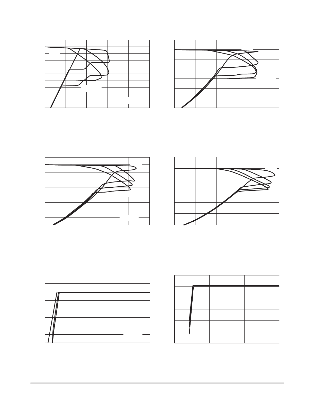
Figure 40. MC78PC30 Line Transient Response Figure 41. MC78PC30 Line Transient Response
3.4
3.3
INPUT VOLTAGE
OUTPUT VOLTAGE
tr = tf = 5.0 ms
C
= 4.7 mF (TANTALUM)
OUT
I
= 30 mA
OUT
, OUTPUT VOLTAGE (VOLTS)
OUT
V
3.2
3.1
3.0
2.9
2.8
0
20 40 60 80 100 120
t, TIME (ms)
Figure 42. MC78PC30 Line Transient Response
3.4
3.3
3.2
INPUT VOLTAGE
6.0
5.0
4.0
6.0
5.0
4.0
3.0
2.0
1.0
0
3.4
V
IN
3.3
, INPUT VOLTAGE (VOLTS)
3.2
3.1
3.0
, OUTPUT VOLTAGE (VOLTS)
2.9
OUT
V
2.8
0
20 40 60 80 100 120
t, TIME (ms)
INPUT VOLTAGE
tr = tf = 5.0 ms
C
= 6.8 mF (TANTALUM)
OUT
I
= 30 mA
OUT
Figure 43. MC78PC30 Load Transient Response
3.4
V
IN
3.3
, INPUT VOLTAGE (VOLTS)
3.2
OUTPUT CURRENT
OUTPUT VOLTAGE
150
100
50
6.0
5.0
4.0
3.0
2.0
1.0
0
V
IN
, INPUT VOLTAGE (VOLTS)
I
OUT
, OUTPUT CURRENT (mA)
3.1
3.0
, OUTPUT VOLTAGE (VOLTS)
2.9
OUT
V
2.8
2.0 4.0 6.0 8.0 10 12
0
t, TIME (ms)
OUTPUT VOLTAGE
CIN = 1.0 mf (TANTALUM)
C
= 4.7 mF (TANTALUM)
OUT
VIN = 4.0 V
14 16 18 20
, OUTPUT VOLTAGE (VOLTS)
OUT
V
3.1
3.0
2.9
2.8
3.0
OUTPUT VOLTAGE
tr = tf = 5.0 ms
C
= 10 mF (TANTALUM)
OUT
I
= 30 mA
OUT
0
20 40 60 80 100 120
t, TIME (ms)
2.0
1.0
0
Figure 44. MC78PC30 Load Transient Response Figure 45. MC78PC30 Load Transient Response
I
OUT
, OUTPUT CURRENT (mA)
3.4
3.3
3.2
3.1
3.0
, OUTPUT VOLTAGE (VOLTS)
2.9
OUT
V
2.8
0
2.0 4.0 6.0 8.0 10 12
t, TIME (ms)
OUTPUT CURRENT
OUTPUT VOLTAGE
CIN = 1.0 mf (TANTALUM)
C
= 10 mF (TANTALUM)
OUT
VIN = 4.0 V
14 16 18 20
3.4
3.3
3.2
3.1
3.0
, OUTPUT VOLTAGE (VOLTS)
2.9
OUT
V
2.8
0
2.0 4.0 6.0 8.0 10 12
t, TIME (ms)
OUTPUT CURRENT
OUTPUT VOLTAGE
CIN = 1.0 mf (TANTALUM)
C
= 6.8 mF (TANTALUM)
OUT
VIN = 4.0 V
14 16 18 20
150
100
50
0
–50
–100
–150
0
–50
–100
–150
150
100
50
0
–50
–100
–150
I
OUT
, OUTPUT CURRENT (mA)
http://onsemi.com
11
Page 12

MC78PC00 Series
APPLICATION HINTS
When using these circuits, please be sure to observe the
following points:
• Phase compensation is made for securing stable operation
even if the load current varies. For this reason, be sure to
use a capacitor C
with good frequency characteristics
OUT
and ESR (Equivalent Series Resistance) as described in
the graphs on page 11.
On page 11, the relations between I
Figure 46. Measuring Circuit for White Noise: MC78PC30
4.0 V
CERAMIC
CAPACITOR
(Output Current)
OUT
V
1.0 mF
3
1
IN
2 GND
CE
and ESR of Output Capacitor are shown. The conditions
where the white noise level is under 40 mV (Avg.) are
marked by the shaded area in the graph. (note: When
additional ceramic capacitors are connected to the Output
Pin with Output capacitor for phase compensation, there
is a possibility that the operation will be unstable. Because
of this, test these circuits with as same external
components as ones to be used on the PCB).
5
V
ESR
OUT
CERAMIC
CAPACITOR
I
OUT
S.A.
SPECTRUM
ANALYSER
MEASURING CONDITIONS: (1) FREQUENCY RANGE: 10 Hz TO 1.0 MHz
MEASURING CONDITIONS: (2) TEMPERATURE: 25°C
• Please be sure the Vin and GND lines are sufficiently
wide. When the impedance of these lines is high, there is
a chance to pick up noise or to malfunction.
• Connect the capacitor with a capacitance of 1.0 mF or
more between Vin and GND as close as possible to Vin or
GND.
Figure 47. T ypical Application
IN
+
CAP.
V
IN
MC78PCxx
• Set external components, especially the Output Capacitor ,
as close as possible to the circuit, and make the wiring as
short as possible.
CE
OUT
GND
V
OUT
+
CAP.
http://onsemi.com
12
Page 13

MC78PC00 Series
E
R
(
)
OUT
Figure 48. Ceramic Capacitor 4.7 mF
100
10
W
S
1.0
0.1
0
50 100 150
I
, OUTPUT CURRENT (mA)
OUT
100
10
W
ESR ( )
1.0
0.1
Figure 49. Ceramic Capacitor 6.8 mF
0
50 100 150
I
, OUTPUT CURRENT (mA)
OUT
Figure 50. Ceramic Capacitor 10 mF
100
10
W
ESR ( )
1.0
0.1
0
50 100 150
I
, OUTPUT CURRENT (mA)
http://onsemi.com
13
Page 14

T APE AND REEL INFORMATION
Component Taping Orientation for 5L SOT–23 Devices
DEVICE
MARKING
MC78PC00 Series
USER DIRECTION OF FEED
PIN 1
Tape & Reel Specifications Table
Package Tape Width (W) Pitch (P) Part Per Full Reel Reel Diameter
5L SOT–23
Standard Reel Component Orientation
for TR Suffix Device
(Mark Right Side Up)
8 mm 4 mm 3000 7 inches
http://onsemi.com
14
Page 15

MC78PC00 Series
P ACKAGE DIMENSIONS
SOT–23–5
N SUFFIX
PLASTIC PACKAGE
CASE 1212–01
ISSUE O
NOTES:
1. DIMENSIONS ARE IN MILLIMETERS.
2. INTERPRET DIMENSIONS AND TOLERANCES
PER ASME Y14.5M, 1994.
3. DATUM C IS A SEATING PLANE.
MILLIMETERS
DIM MIN MAX
A1 0.00 0.10
A2 1.00 1.30
B 0.30 0.50
C 0.10 0.25
D 2.80 3.00
E 2.50 3.10
E1 1.50 1.80
e 0.95 BSC
e1 1.90 BSC
L
0.20 –––
L1 0.45 0.75
A
E
D
1523
B
4
0.05
A2
S
A1
L
E1
L1
B 5X
M
e
0.10 CSBSA
C
C
e1
Recommended Footprint for SOT–23–5 Surface Mount Applications
0.7 MAX.
1.0
0.950.95
1.9
SOT–23–5
2.4
(Unit: mm)
http://onsemi.com
15
Page 16

MC78PC00 Series
ON Semiconductor and are trademarks of Semiconductor Components Industries, LLC (SCILLC). SCILLC reserves the right to make changes
without further notice to any products herein. SCILLC makes no warranty , representation or guarantee regarding the suitability of its products for any particular
purpose, nor does SCILLC assume any liability arising out of the application or use of any product or circuit, and specifically disclaims any and all liability ,
including without limitation special, consequential or incidental damages. “Typical” parameters which may be provided in SCILLC data sheets and/or
specifications can and do vary in different applications and actual performance may vary over time. All operating parameters, including “Typicals” must be
validated for each customer application by customer’s technical experts. SCILLC does not convey any license under its patent rights nor the rights of others.
SCILLC products are not designed, intended, or authorized for use as components in systems intended for surgical implant into the body, or other applications
intended to support or sustain life, or for any other application in which the failure of the SCILLC product could create a situation where personal injury or
death may occur. Should Buyer purchase or use SCILLC products for any such unintended or unauthorized application, Buyer shall indemnify and hold
SCILLC and its officers, employees, subsidiaries, affiliates, and distributors harmless against all claims, costs, damages, and expenses, and reasonable
attorney fees arising out of, directly or indirectly , any claim of personal injury or death associated with such unintended or unauthorized use, even if such claim
alleges that SCILLC was negligent regarding the design or manufacture of the part. SCILLC is an Equal Opportunity/Affirmative Action Employer .
PUBLICATION ORDERING INFORMATION
USA/EUROPE Literature Fulfillment:
Literature Distribution Center for ON Semiconductor
P.O. Box 5163, Denver, Colorado 80217 USA
Phone: 303–675–2175 or 800–344–3860 Toll Free USA/Canada
Fax: 303–675–2176 or 800–344–3867 Toll Free USA/Canada
Email: ONlit@hibbertco.com
Fax Response Line*: 303–675–2167
800–344–3810 Toll Free USA/Canada
*To receive a Fax of our publications
N. America Technical Support: 800–282–9855 Toll Free USA/Canada
http://onsemi.com
ASIA/PACIFIC: LDC for ON Semiconductor – Asia Support
Phone: 303–675–2121 (Tue–Fri 9:00am to 1:00pm, Hong Kong T ime)
Email: ONlit–asia@hibbertco.com
JAPAN: ON Semiconductor, Japan Customer Focus Center
4–32–1 Nishi–Gotanda, Shinagawa–ku, T okyo, Japan 141–8549
Phone: 81–3–5487–8345
Email: r14153@onsemi.com
ON Semiconductor Website: http://onsemi.com
For additional information, please contact your local Sales Representative.
MC78PC00/D
16
 Loading...