

Datasheet MC78LC40NTR, MC78LC50HT1, MC78LC40HT1, MC78LC33NTR, MC78LC33HT1 Datasheet (Motorola)
...Page 1
Order this document by MC78LC00/D
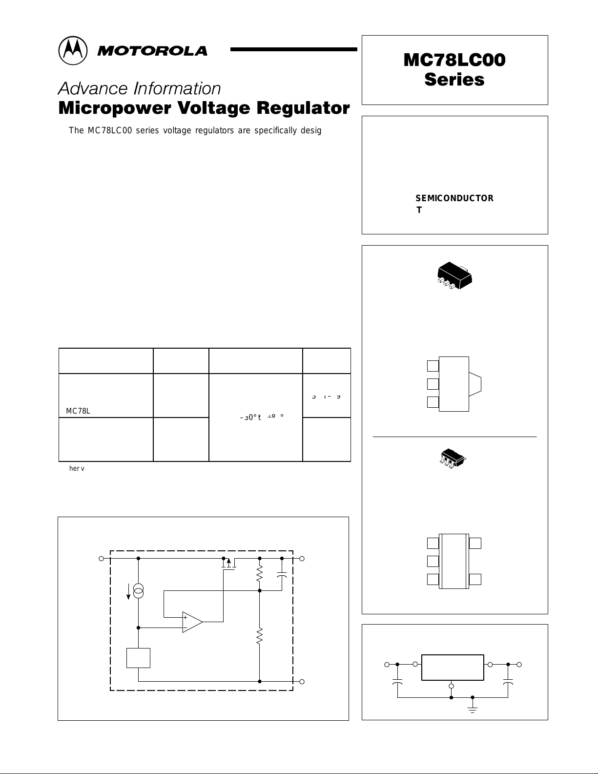
SOT–89
T
30° t
80°C
SOT–23
The MC78LC00 series voltage regulators are specifically designed for
use as a power source for video instruments, handheld communication
equipment, and battery powered equipment.
The MC78LC00 series features an ultra–low quiescent current of 1.1 µA
and a high accuracy output voltage. Each device contains a voltage
reference, an error amplifier, a driver transistor and resistors for setting the
output voltage. These devices are available in either SOT–89, 3 pin, or
SOT–23, 5 pin, surface mount packages.
MC78LC00 Series Features:
• Low Quiescent Current of 1.1 µA Typical
• Low Dropout Voltage (220 mV at 10 mA)
• Excellent Line Regulation (0.1%)
• High Accuracy Output Voltage (±2.5%)
• Wide Output Voltage Range (2.0 V to 6.0 V)
• Output Current for Low Power (up to 80 mA)
• Two Surface Mount Packages (SOT–89, 3 Pin, or SOT–23, 5 Pin)
ORDERING INFORMATION
Output
Device
MC78LC30HT1 3.0
MC78LC33HT1 3.3
MC78LC40HT1 4.0
MC78LC50HT1 5.0
MC78LC30NTR 3.0
MC78LC33NTR 3.3
MC78LC40NTR 4.0
MC78LC50NTR 5.0
Other voltages from 2.0 to 6.0 V, in 0.1 V increments, are available upon request. Consult
factory for information.
Voltage
Representative Block Diagram
2
V
in
Operating
Temperature Range
°
A
= –
o +
°
Package
3
V
O
–
–
MICROPOWER ULTRA–LOW
QUIESCENT CURRENT
VOLTAGE REGULATORS
SEMICONDUCTOR
TECHNICAL DATA
TAB
1
H SUFFIX
PLASTIC PACKAGE
CASE 1213
(SOT–89)
1
Ground
2
Input
3
Output
(Top View)
5
1
N SUFFIX
PLASTIC PACKAGE
CASE 1212
(SOT–23)
Ground
15
Input
2
Tab
(Tab is connected
to Pin 2)
N/C
V
ref
This device contains 8 active transistors.
This document contains information on a new product. Specifications and information herein
are subject to change without notice.
MOTOROLA ANALOG IC DEVICE DATA
N/C
Output
3
(Top View)
4
Standard Application
Input Output
1
Gnd
Motorola, Inc. 1997 Rev 1
C
in
2
MC78LCXX
1
3
C
O
1
Page 2
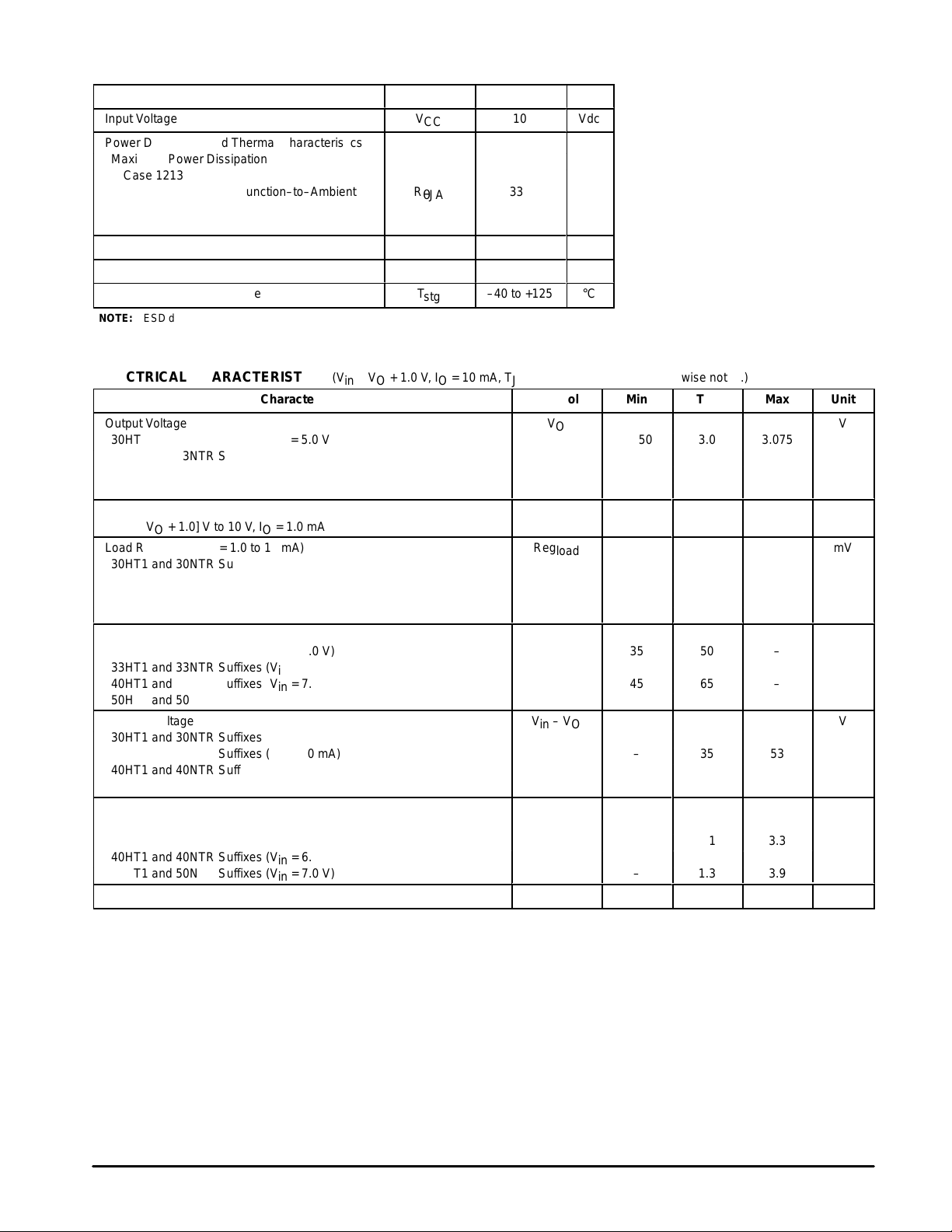
MAXIMUM RATINGS
ÁÁÁ
ÁÁÁ
ÁÁÁ
ÁÁÁ
ÁÁÁ
ÁÁÁ
Á
Á
Á
Á
Á
ÁÁÁ
Á
Rating Symbol Value Unit
Input Voltage
Power Dissipation and Thermal Characteristics
Maximum Power Dissipation
Case 1213 (SOT–89) H Suffix P
Thermal Resistance, Junction–to–Ambient R
Case 1212 (SOT–23) N Suffix P
Thermal Resistance, Junction–to–Ambient R
Operating Junction Temperature
Operating Ambient Temperature
Storage Temperature Range
NOTE: ESD data available upon request.
MC78LC00 Series
V
T
CC
θJA
θJA
T
T
stg
D
D
J
A
10
300 mW
333 °C/W
150 mW
667 °C/W
125
–30 to +80
–40 to +125
Vdc
°C
°C
°C
ELECTRICAL CHARACTERISTICS (V
Characteristic
Output Voltage
= VO + 1.0 V, IO = 10 mA, TJ = 25°C [Note 1], unless otherwise noted.)
in
Symbol Min Typ Max Unit
V
O
30HT1 and 30NTR Suffixes (Vin = 5.0 V) 2.950 3.0 3.075
33HT1 and 33NTR Suffixes (Vin = 5.0 V) 3.218 3.3 3.382
40HT1 and 40NTR Suffixes (Vin = 6.0 V) 3.900 4.0 4.100
50HT1 and 50NTR Suffixes (Vin = 7.0 V) 4.875 5.0 5.125
Line Regulation
Reg
line
–
0.05
Vin = [VO + 1.0] V to 10 V, IO = 1.0 mA
Load Regulation (IO = 1.0 to 10 mA)
Reg
load
30HT1 and 30NTR Suffixes (Vin = 5.0 V) – 40 60
33HT1 and 33NTR Suffixes (Vin = 6.0 V) – 40 60
40HT1 and 40NTR Suffixes (Vin = 7.0 V) – 50 70
50HT1 and 50NTR Suffixes (Vin = 8.0 V) – 60 90
Output Current
I
O
30HT1 and 30NTR Suffixes (Vin = 5.0 V) 35 50 –
33HT1 and 33NTR Suffixes (Vin = 6.0 V) 35 50 –
40HT1 and 40NTR Suffixes (Vin = 7.0 V) 45 65 –
50HT1 and 50NTR Suffixes (Vin = 8.0 V) 55 80 –
Dropout Voltage
Vin – V
O
30HT1 and 30NTR Suffixes (IO = 1.0 mA) – 40 60
33HT1 and 33NTR Suffixes (IO = 1.0 mA) – 35 53
40HT1 and 40NTR Suffixes (IO = 1.0 mA) – 25 38
50HT1 and 50NTR Suffixes (IO = 1.0 mA) – 25 38
Quiescent Current
I
CC
30HT1 and 30NTR Suffixes (Vin = 5.0 V) – 1.1 3.3
33HT1 and 33NTR Suffixes (Vin = 5.0 V) – 1.1 3.3
40HT1 and 40NTR Suffixes (Vin = 6.0 V) – 1.2 3.6
50HT1 and 50NTR Suffixes (Vin = 7.0 V) – 1.3 3.9
Output Voltage Temperature Coefficient
БББББББББББББББББ
NOTE: 1.Low duty pulse techniques are used during test to maintain junction temperature as close to ambient as possible.
T
C
ÁÁÁ
–
ÁÁ
±100
ÁÁ
0.2
–
ÁÁ
V
mV
mV
mA
V
µA
ppm/°C
ÁÁ
2
MOTOROLA ANALOG IC DEVICE DATA
Page 3
MC78LC00 Series
DEFINITIONS
Dropout Voltage – The input/output voltage differential at
which the regulator output no longer maintains regulation
against further reductions in input voltage. Measured when
the output drops 100 mV below its nominal value (which is
measured at 1.0 V differential), dropout voltage is affected
by junction temperature, load current and minimum input
supply requirements.
Line Regulation – The change in output voltage for a change
in input voltage. The measurement is made under conditions
Figure 1. Output V oltage versus Input Voltage
3.2
3.0
IO = 1.0 mA
2.8
2.6
, OUTPUT VOL TAGE (V)V
O
V
2.4
IO = 10 mA
2.2
2.5
2.7
IO = 5.0 mA
2.9 3.1 3.3
Vin, INPUT VOLTAGE (V)
TA = 25°C
3.5
of low dissipation or by using pulse techniques such that
average chip temperature is not significantly affected.
Load Regulation – The change in output voltage for a
change in load current at constant chip temperature.
Maximum Power Dissipation – The maximum total device
dissipation for which the regulator will operate within
specifications.
Quiescent Bias Current – Current which is used to operate
the regulator chip and is not delivered to the load.
Figure 2. Output Voltage versus Output Current
3.2
3.1
80
TA = –30°C
100
120
3.0
2.9
TA = 25
°
2.8
, OUTPUT VOL TAGE (V)V
O
V
2.7
MC78LC30NTRMC78LC30NTR
0
0
20
40
IO, OUTPUT CURRENT (mA)
C
TA = 80°C
60
Figure 3. Dropout Voltage versus Output Current Figure 4. Output Voltage versus Temperature
, OUTPUT VOL TAGE (V)
3.10
3.061.6
3.021.2
2.98
O
2.94
2.90
Vin = 5.0 V
IO= 10 mA
–40
20
TA, AMBIENT TEMPERATURE (
40
MC78LC30NTR
°
C)
2.0
0.8
, DROPOUT VOLTAGE (V)
O
–V
0.4
in
0
0
MC78LC30NTR
°
C
TA = 25
10 –20
20
IO, OUTPUT CURRENT (mA)
30 0
40
50
60 80
MOTOROLA ANALOG IC DEVICE DATA
3
Page 4

MC78LC00 Series
Figure 5. Quiescent Current versus Input V oltage
1.4
TA = 25°C
1.3
µ
1.2
1.1
1.0
, QUIESCENT CURRENT ( A)
0.9
CC
I
0.8
3.0
4.0 205.0
Vin, INPUT VOLTAGE (V)
MC78LC30NTR MC78LC30NTR
8.0
Figure 7. Dropout Voltage versus
Set Output Voltage
0.8
0.7
IO = 10 mA
0.6
0.5
0.4
0.3
, DROPOUT VOLTAGE (V)
O
0.2
–V
IO = 1.0 mA
in
V
0.1
0
1.0 2.0
VO, SET OUTPUT VOLTAGE (V)
3.0
4.0
9.0
5.0
10
6.0
Figure 6. Quiescent Current versus T emperature
1.2
Vin = 5.0 V
1.1
µ
1.0
0.9
0.8
, QUIESCENT CURRENT ( A)
0.7
CC
I
0.6
–40
–20
0
TA, AMBIENT TEMPERATURE (
406.0 7.0 60
°
C)
Figure 8. Line Transient Response
8.0
7.5
Input Voltage
Output Voltage
CO = 0.1
IO = 1.0 mA
4.0
t, TIME (ms)
INPUT VOLTAGE/OUTPUT VOL TAGE (V)
7.0
6.5
6.0
5.5
5.0
4.5
4.00
0
2.0
80
µ
F
6.0
4
MOTOROLA ANALOG IC DEVICE DATA
Page 5

MC78LC00 Series
APPLICATIONS INFORMATION
Introduction
The MC78LC00 micropower voltage regulators are
specifically designed with high accuracy output voltage and
ultra low quiescent current by CMOS process making them
ideal for battery powered applications and hand–held
communication equipment. An input bypass capacitor is
recommended if the regulator is located an appreciable
distance (≥ 4 inches) from the input voltage source. These
regulators require ≥ 0.1 µF capacitance between the output
terminal and ground for stability. Most types of aluminum,
tantalum or multilayer ceramic will perform adequately. Solid
tantalums or other appropriate capacitors are recommended
for operation below 25°C. The bypass capacitors should be
mounted with the shortest possible leads or track lengths
directly across the regulator input and output terminals.
With economical electrolytic capacitors, cold temperature
operation can pose a serious stability problem. As the
electrolyte freezes, around –30°C, the capacitance will
decrease and the equivalent series resistance (ESR) will
increase drastically, causing the circuit to oscillate. Quality
electrolytic capacitors with extended temperature ranges of
–40° to +85°C are readily available. Solid tantalum
capacitors may be the better choice if small size is a
requirement. However, a maximum ESR limit of 3.0 Ω must
be observed over temperature to maintain stability .
In the Current Boost Circuit, shown in Figures 10 and 12,
an output current of up to 600 mA can be delivered by the
circuit. The circuit of Figure 10 has no current limit. In each
case, the external transistor must be rated for the expected
power dissipation. Figure 11 shows how a fixed output may
be programmed, using R1 and R2, to provide a higher
output voltage.
V
Gnd
V
in
Figure 9. T ypical Application
in
23
MC78LC00
1
V
O
0.1
µ
F0.1 µF
Gnd
V
in
Gnd
0.1
Figure 10. Current Boost Circuit
MJD32C
.033 µF
100
µ
F
23
MC78LC00
V
O
1
0.1
µ
F
Gnd
Figure 12. Current Boost Circuit with
C1
Figure 11. Adjustable V
23
MC78LC00
1
I
CC
O
R1
Gnd
R2
C2
V
O
V
in
MMBT2907
Overcurrent Limit Circuit
MJD32C
R2
Q2
ALT1
R1
0.1
Q1
µ
F
.033 µF
23
MC78LC00
1
0.1
V
O
µ
F
VO+
V
O(Reg)
ǒ
Ǔ
1
)
)
ICCR2
R1
R2
MOTOROLA ANALOG IC DEVICE DATA
Gnd
V
I
circuit)
O(short
BE2
[
R2
Gnd
V
)
V
BE1
)
BE2
R1
5
Page 6

MC78LC00 Series
OUTLINE DIMENSIONS
H SUFFIX
PLASTIC PACKAGE
CASE 1213–01
(SOT–89)
ISSUE O
A
E
D
D1
B
A2
C
E1
L1
B
M
0.10 CSBSA
C
B1 2X
e
M
0.10 CSBSA
NOTES:
1. DIMENSIONS ARE IN MILLIMETERS.
2. INTERPRET DIMENSIONS AND TOLERANCING
PER ASME Y14.5M, 1994.
3. DATUM C IS A SEATING PLANE.
MILLIMETERS
DIM MIN MAX
A2 1.40 1.60
B 0.37 0.57
B1 0.32 0.52
C 0.30 0.50
D 4.40 4.60
D1 1.50 1.70
E ––– 4.25
E1 2.40 2.60
e 1.50 BSC
e1 3.00 BSC
L1 0.80 –––
e1
N SUFFIX
PLASTIC PACKAGE
CASE 1212–01
(SOT–23)
ISSUE O
A
E
D
1523
B
4
0.05
A2
S
A1
L
E1
L1
B 5X
M
e
0.10 CSBSA
C
C
e1
NOTES:
1. DIMENSIONS ARE IN MILLIMETERS.
2. INTERPRET DIMENSIONS AND TOLERANCES
PER ASME Y14.5M, 1994.
3. DATUM C IS A SEATING PLANE.
MILLIMETERS
DIM MIN MAX
A1 0.00 0.10
A2 1.00 1.30
B 0.30 0.50
C 0.10 0.25
D 2.80 3.00
E 2.50 3.10
E1 1.50 1.80
e 0.95 BSC
e1 1.90 BSC
L
0.20 –––
L1 0.45 0.75
6
MOTOROLA ANALOG IC DEVICE DATA
Page 7

MC78LC00 Series
Motorola reserves the right to make changes without further notice to any products herein. Motorola makes no warranty , representation or guarantee regarding
the suitability of its products for any particular purpose, nor does Motorola assume any liability arising out of the application or use of any product or circuit, and
specifically disclaims any and all liability, including without limitation consequential or incidental damages. “T ypical” parameters which may be provided in Motorola
data sheets and/or specifications can and do vary in different applications and actual performance may vary over time. All operating parameters, including “Typicals”
must be validated for each customer application by customer’s technical experts. Motorola does not convey any license under its patent rights nor the rights of
others. Motorola products are not designed, intended, or authorized for use as components in systems intended for surgical implant into the body, or other
applications intended to support or sustain life, or for any other application in which the failure of the Motorola product could create a situation where personal injury
or death may occur. Should Buyer purchase or use Motorola products for any such unintended or unauthorized application, Buyer shall indemnify and hold Motorola
and its officers, employees, subsidiaries, affiliates, and distributors harmless against all claims, costs, damages, and expenses, and reasonable attorney fees
arising out of, directly or indirectly, any claim of personal injury or death associated with such unintended or unauthorized use, even if such claim alleges that
Motorola was negligent regarding the design or manufacture of the part. Motorola and are registered trademarks of Motorola, Inc. Motorola, Inc. is an Equal
Opportunity/Affirmative Action Employer.
MOTOROLA ANALOG IC DEVICE DATA
7
Page 8

MC78LC00 Series
How to reach us:
USA/EUROPE/Locations Not Listed: Motorola Literature Distribution; JAPAN: Nippon Motorola Ltd.: SPD, Strategic Planning Office, 4–32–1,
P.O. Box 5405, Denver, Colorado 80217. 303–675–2140 or 1–800–441–2447 Nishi–Gotanda, Shinagawa–ku, Tokyo 141, Japan. 81–3–5487–8488
Mfax: RMFAX0@email.sps.mot.com – TOUCHTONE 602–244–6609 ASIA/PACIFIC: Motorola Semiconductors H.K. Ltd.; 8B Tai Ping Industrial Park,
INTERNET: http://motorola.com/sps
8
– US & Canada ONLY 1–800–774–1848 51 Ting Kok Road, T a i Po, N.T., Hong Kong. 852–26629298
◊
MOTOROLA ANALOG IC DEVICE DATA
Mfax is a trademark of Motorola, Inc.
MC78LC00/D
 Loading...