

Datasheet MC78L24A, MC78L18A, MC78L15A, MC78L12A, MC78L05AA Datasheet (Fairchild Semiconductor)
...Page 1
www.fairchildsemi.com
MC78LXXA/LM78LXXA/MC78L05AA
3-Terminal 0.1A Positive Voltage Regulator
Features
• Maximum Output Current of 100mA
• Output Voltage of 5V, 8V, 12V, 15V, 18V and 24V
• Thermal Overload Protection
• Short Circuit Current Limiting
• Output Voltage Offered in ±5% Tolerance
Description
The MC78LXXA/LM78LXXA/MC78L05AA series of
fixed voltage monolithic integrated circuit voltage
regulators are suitable for application that required supply
current up to 100mA.
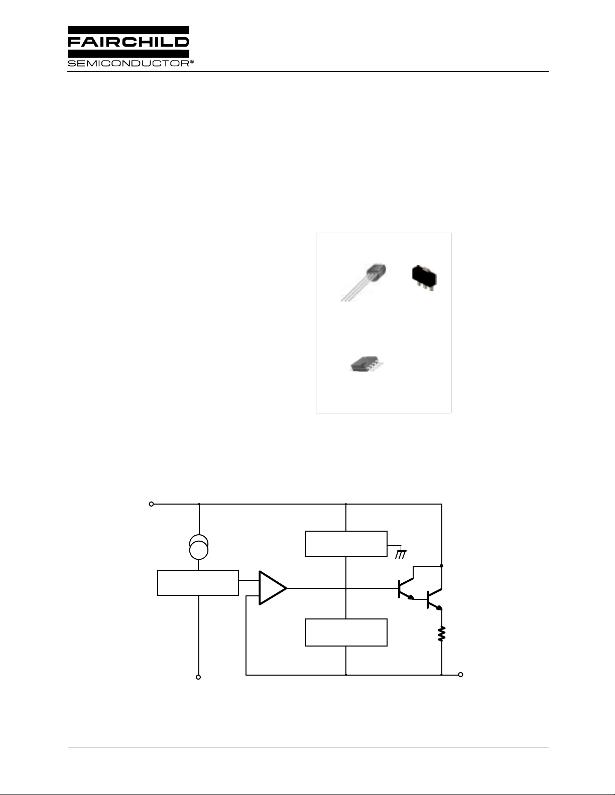
TO-92
2
1
3
1. Output 2. GND 3. Input
8-SOP
8
1. Output 2. GND 3. GND 4. NC
5. NC 6. GND 7. GND 8. Input
SOT-89
GND
1
23
1
Internal Block Diagram
V
I
Inpu
t
3
REFERE NCE VOLT AGE
GND
2
©2002 Fairchild Semiconductor Corporation
THERMAL SHUTDOWN
I
+
-
CIRCUIT
SHORT CIRCUIT
PROTECTION
R
SC
V
0
Outpu
1
t
Rev. 1.0.4
Page 2
MC78LXXA/LM78LXXA/MC78L05AA
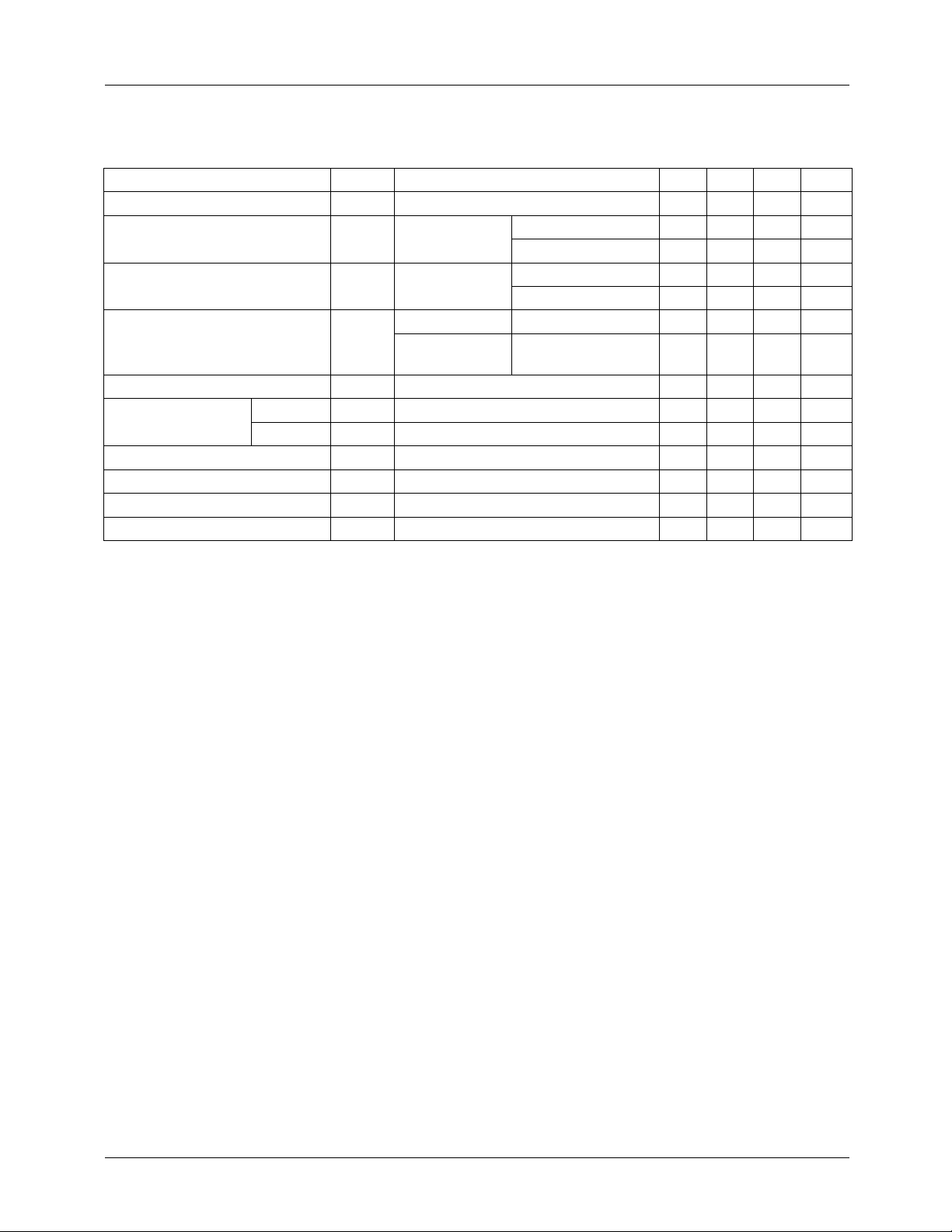
Absolute Maximum Ratings
Parameter Symbol Value Unit
Input Voltage (for V
(for V
= 12V to 18V)
O
(for V
O =
24V)
= 5V, 8V)
O
Operating Junction Temperature Range T
Storage Temperature Range T
V
I
J
STG
30
35
40
0 ~ +150 °C
-65 ~ +150 °C
V
V
V
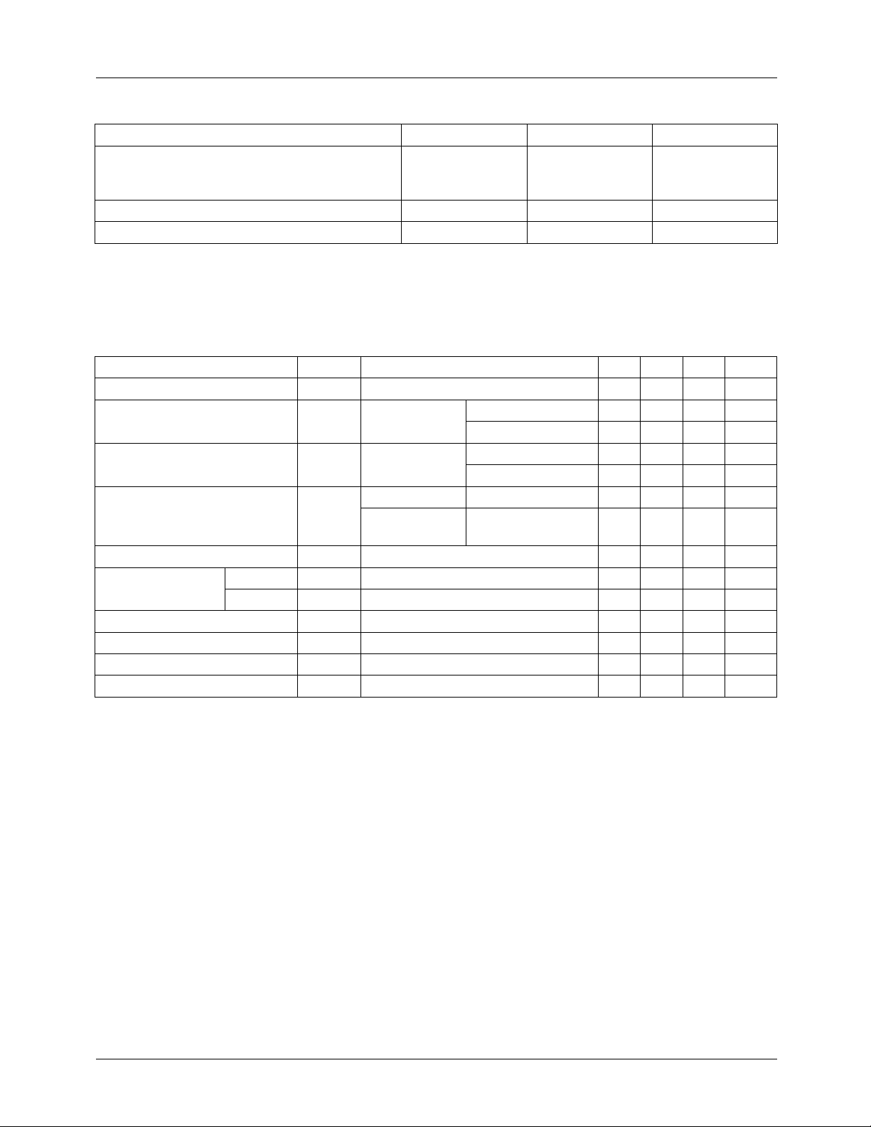
Electrical Characteristics(MC78L05A/LM78L05A)
(V
= 10V, I
I
Parameter Symbol Conditions Min. Typ. Max. Unit
Output Voltage V
Line Regulation (Note1)
Load Regulation (Note1)
Output Voltage V
Quiescent Current I
Quiescent Current
Change
Output Noise Voltage V
Temperature Coefficient of V
Ripple Rejection RR f = 120Hz, 8V ≤ V
Dropout Voltage V
= 40mA, 0°C
O
≤ T
≤ 125°C, CI = 0.33µF, CO = 0.1µF, unless otherwise specified. (Note 1)
J
∆V
∆V
With Line ∆I
With Load ∆I
∆V
O
TJ = 25°C4.85.05.2V
O
TJ = 25°C
O
O
TJ = 25°C
7V ≤ V
O
7V ≤ V
≤ 20V 1mA ≤ IO ≤ 40mA - - 5.25 V
I
≤ V
I
(Note 2)
TJ = 25°C-2.05.5mA
Q
8V ≤V
Q
1mA ≤ I
Q
TA = 25°C, 10Hz ≤ f ≤ 100kHz - 40 - µV/Vo
N
/∆TIO = 5mA - -0.65 - mV/°C
O
TJ = 25°C-1.7-V
D
≤ 20V - - 1.5 mA
I
≤ 40
O
7V ≤≤≤≤ V
8V ≤≤≤≤ V
1mA ≤ I
1mA ≤ I
MAX
1mA ≤ I
mA - - 0.1 mA
I
≤≤≤≤ 20V - 8 150 mV
I
≤≤≤≤ 20V - 6 100 mV
I
≤ 100mA - 11 60 mV
O
≤ 40mA - 5.0 30 mV
O
≤ 70mA 4.75 - 5.25 V
O
≤ 18V, T
= 25°C4180 - dB
J
Note:
1. The max imum st eady sta te usable output cu rrent and inpu t voltage are very depende nt on the heat si nking an d/or lead length
of the package. The data a bove rep resent p ulse tes t conditi ons with junction temper ature as indicate d at the initiatio n of test s.
2. Power dissipation P
≤ 0.75W.
D
2
Page 3
MC78LXXA/LM78LXXA/MC78L05AA
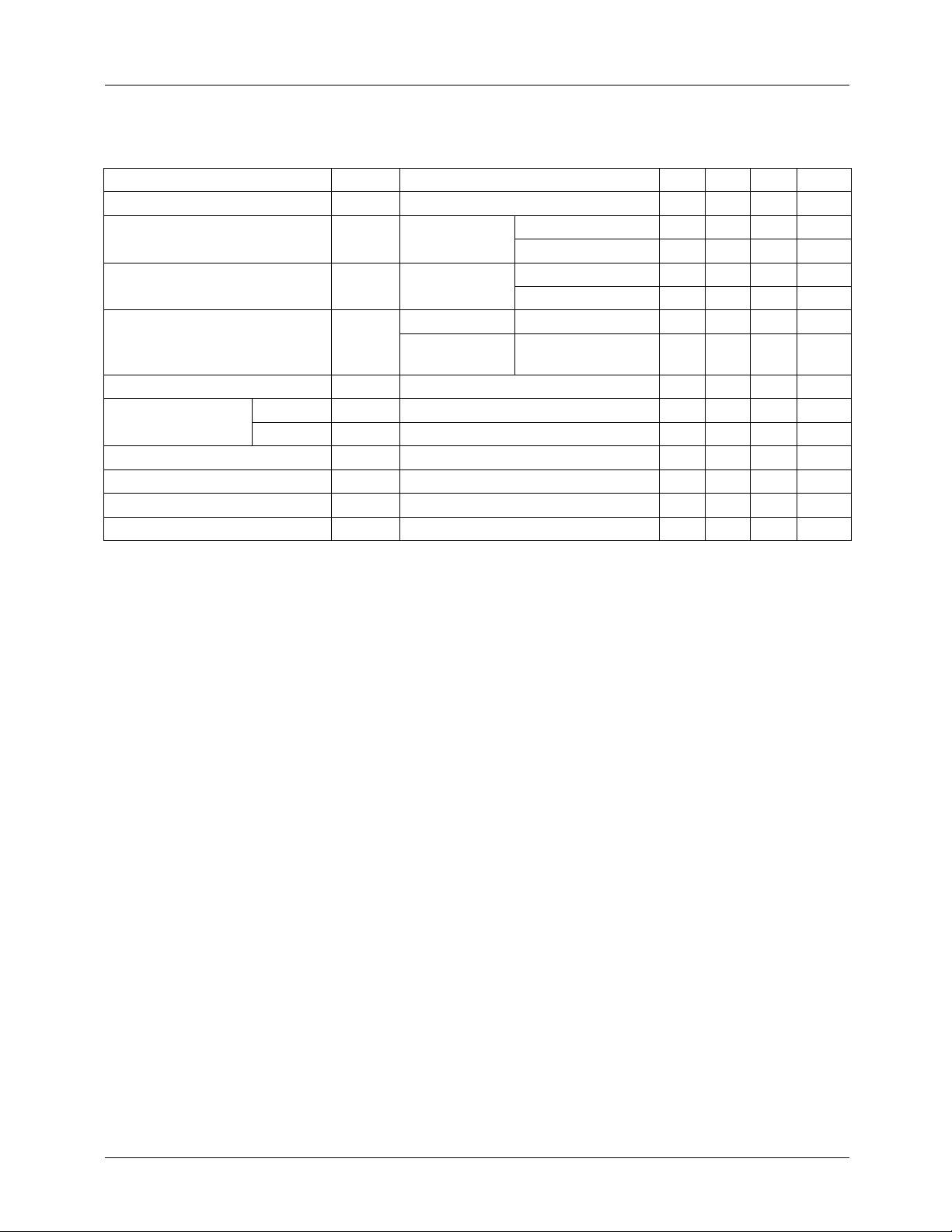
Electrical Characteristics(MC78L08A)
(V
I
= 14V, I
= 40mA, 0°C ≤ TJ ≤ 125°C, CI = 0.33µF, CO = 0.1µF, unless otherwise specified. (Note 1)
O
(Continued)
Parameter Symbol Conditions Min. Typ. Max. Unit
Output Voltage V
Line Regulation (Note1) ∆V
Load Regulation (Note1) ∆V
Output Voltage V
Quiescent Current I
Quiescent Current
Change
With Line ∆I
With Load ∆I
Q
Output Noise Voltage V
Temperature Coefficient of V
∆V
O
O
Ripple Rejection RR f = 120Hz, 11V ≤ V
Dropout Voltage V
Note:
1. The ma ximum ste ady stat e usable output curre nt and input vo ltage ar e very d epende nt on th e heat s inking a nd/or lead le ngth
of the package. The dat a above repres ent pulse test c onditions with junction temp erature as ind icated at the initi ation of tests.
2. Power dissipation P
≤ 0.75W.
D
TJ = 25°C 7.7 8.0 8.3 V
O
TJ = 25°C
O
TJ = 25°C1mA ≤ I
O
O
10.5V ≤ V
10.5V ≤ V
V
MAX
I
I
(Note 2)
10.5V ≤ V
11V ≤ V
1mA ≤ I
≤ 23V 1mA ≤ IO ≤ 40mA 7.6 - 8.4 V
≤
1mA ≤ I
≤ 23V - 10 175 mV
I
≤ 23V - 8 125 mV
I
≤ 100mA - 15 80 mV
O
≤ 40mA - 8.0 40 mV
O
≤ 70mA 7.6 - 8.4 V
O
TJ = 25°C-2.05.5mA
11V ≤ V
Q
1mA ≤ I
Q
TA = 25°C, 10Hz ≤ f ≤100kHz - 60 - µV/Vo
N
/∆TIO = 5mA - -0.8 - mV/
TJ = 25°C-1.7-V
D
≤ 23V - - 1.5 mA
I
≤ 40mA - - 0.1 mA
O
≤ 21V, T
I
= 25°C39 70 - dB
J
°C
3
Page 4
MC78LXXA/LM78LXXA/MC78L05AA
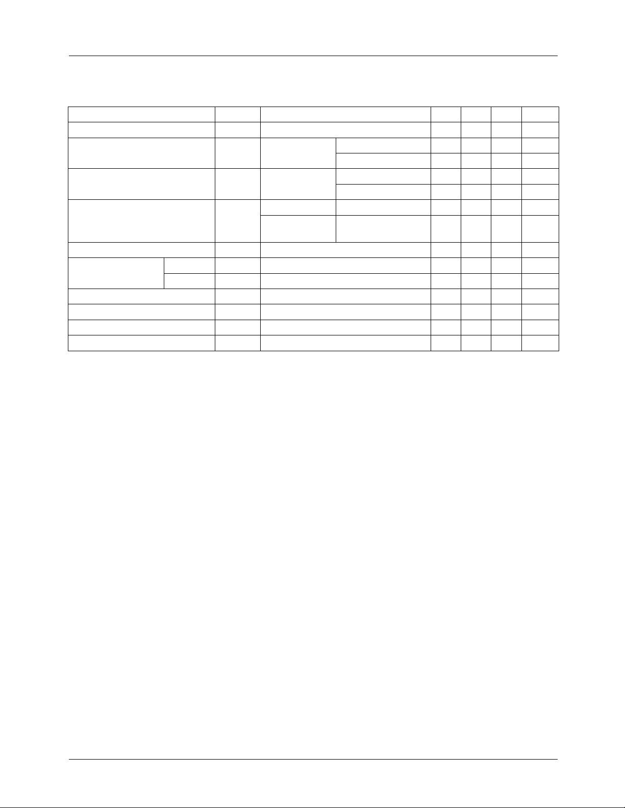
Electrical Characteristics(MC78L12A/LM78L12A)
(V
I
= 19V, I
= 40mA, 0°C ≤ TJ ≤ 125°C, CI = 0.33 µF, CO = 0.1µF, unless otherwise specified. (Note 1)
O
(Continued)
Parameter Symbol Conditions Min. Typ. Max. Unit
Output Voltage V
Line Regulation (Note1) ∆V
Load Regulation (Note1) ∆V
Output Voltage V
Quiescent Current I
Quiescent Current
Change
With Line ∆I
With Load ∆I
Output Noise Voltage V
Temperature Coefficient of V
∆V
O
O
Ripple Rejection RR f = 120Hz, 15V ≤ V
Dropout Voltage V
Note:
1. The ma ximum ste ady stat e usable output curre nt and input vo ltage ar e very d epende nt on th e heat s inking a nd/or lead le ngth
of the package. The dat a above repres ent pulse test c onditions with junction temp erature as ind icated at the initi ation of tests.
2. Power dissipation P
≤ 0.75W.
D
TJ = 25°C 11.5 12 12.5 V
O
≤
14.5V ≤ V
16V ≤ V
1mA ≤ I
1mA ≤ I
1mA ≤ I
TJ = 25°C
O
TJ = 25°C
O
14.5V ≤ V
O
14.5V ≤ V
V
MAX
TJ = 25°C-2.16.0mA
Q
16V ≤ V
Q
1mA ≤ I
Q
TA = 25°C, 10Hz ≤ f ≤ 100kHz - 80 - µV/Vo
N
≤ 27V 1mA ≤ IO ≤ 40mA 11.4 - 12.6 V
I
I
(Note 2)
≤ 27V - - 1.5 mA
I
≤ 40mA - - 0.1 mA
O
≤ 27V - 20 250 mV
I
≤ 27V - 15 200 mV
I
≤ 100mA - 20 100 mV
O
≤ 40mA - 10 50 mV
O
≤ 70mA 11.4 - 12.6 V
O
/∆TIO = 5mA - -1.0 - mV/°C
≤ 25V, T
I
TJ = 25°C-1.7-V
D
= 25°C37 65 - dB
J
4
Page 5
MC78LXXA/LM78LXXA/MC78L05AA
Electrical Characteristics(MC78L15A)
(V
I
= 23V, I
= 40mA, 0°C ≤ TJ ≤ 125°C, CI = 0.33 µF, CO = 0.1µF, unless otherwise specified. (Note 1)
O
(Continued)
Parameter Symbol Conditions Min. Typ. Max. Unit
Output Voltage V
Line Regulation (Note1) ∆V
Load Regulation (Note1) ∆V
Output Voltage V
Quiescent Current I
Quiescent Current
Change
With Line ∆I
With Load ∆I
Output Noise Voltage V
Temperature Coefficient of V
∆V
O
O
Ripple Rejection RR f = 120Hz, 18.5V≤V
Dropout Voltage V
Note:
1. The maximum s tea dy state usable output cur re nt and input voltage are very dependent on the heat sinking and/or le ad le ngth
of the package. The data a bove rep resent p ulse tes t conditi ons with junction temper ature as indicate d at the initiatio n of test s.
2. Power dissipation P
≤ 0.75W.
D
TJ = 25°C 14.4 15 15.6 V
O
≤
17.5V ≤ V
20V ≤ V
1mA ≤ I
1mA ≤ I
1mA ≤ I
TJ = 25°C
O
TJ = 25°C
O
17.5V ≤ V
O
17.5V ≤ V
V
MAX
TJ = 25°C-2.16.0mA
Q
20V ≤ V
Q
1mA ≤ I
Q
TA = 25°C, 10Hz ≤ f ≤ 100kHz - 90 - µV/Vo
N
≤ 30V 1mA ≤ IO ≤ 40mA 14.25 - 15.75 V
I
I
(Note 2)
≤ 30V - - 1.5 mA
I
≤ 40mA - - 0.1 mA
O
≤ 30V - 25 300 mV
I
≤ 30V - 20 250 mV
I
≤ 100mA - 25 150 mV
O
≤ 40mA - 12 75 mV
O
≤ 70mA 14.25 - 15.75 V
O
/∆TIO = 5mA - -1.3 - mV/°C
≤28.5V, T
I
TJ = 25°C-1.7-V
D
= 25°C34 60 - dB
J
5
Page 6

MC78LXXA/LM78LXXA/MC78L05AA
Electrical Characteristics(MC78L18A)
(V
I
= 27V, I
= 40mA, 0°C ≤ TJ ≤ 125°C, CI = 0.33µF, CO = 0.1µF, unless otherwise specified. (Note 1)
O
(Continued)
Parameter Symbol Conditions Min. Typ. Max. Unit
Output Voltage V
Line Regulation (Note1) ∆V
Load Regulation (Note1) ∆V
Output Voltage V
Quiescent Current I
Quiescent Current
Change
With Line ∆I
With Load ∆I
Output Noise Voltage V
Temperature Coefficient of V
∆V
O
O
Ripple Rejection RR f = 120Hz, 23V ≤ V
Dropout Voltage V
Note:
1. The maximum stead y state usable ou tp ut curre nt and inp ut volta ge ar e very de pende nt on the heat sinking and/ or lead le ngth
of the package. The dat a above repres ent pulse test c onditions with junction temp erature as ind icated at the i nitiation of test s.
2. Power dissipation P
≤ 0.75W.
D
TJ = 25°C 17.3 18 18.7 V
O
TJ = 25°C
O
TJ = 25°C
O
21V ≤ V
O
21V ≤ V
V
MAX
TJ = 25°C-2.26.0mA
Q
21V ≤ V
Q
1mA ≤ I
Q
TA = 25°C, 10Hz ≤ f ≤ 100kHz - 150 - µV/Vo
N
≤ 33V 1mA ≤ IO ≤ 40mA 17.1 - 18.9 V
I
≤
I
(Note 2)
≤ 33V - - 1.5 mA
I
≤ 40mA - - 0.1 mA
O
21V ≤ V
22V ≤ V
1mA ≤ I
1mA ≤ I
1mA ≤ I
≤ 33V - 145 300 mV
I
≤ 33V - 135 250 mV
I
≤100mA - 30 170 mV
O
≤ 40mA - 15 85 mV
O
≤ 70mA 17.1 - 18.9 V
O
/∆TIO = 5mA - -1.8 - mV/°C
≤ 33V, T
I
TJ = 25°C-1.7-V
D
= 25°C34 48 - dB
J
6
Page 7

MC78LXXA/LM78LXXA/MC78L05AA
Electrical Characteristics(MC78L24A)
(V
I
= 33V, I
= 40mA, 0°C ≤ TJ ≤ 125°C, CI = 0.33µF, CO = 0.1µF, unless otherwise specified. (Note 1)
O
(Continued)
Parameter Symbol Conditions Min. Typ. Max. Unit
Output Voltage V
Line Regulation (Note1)
∆V
Load Regulation (Note1) ∆V
Output Voltage V
Quiescent Current I
Quiescent Current
Change
With Line ∆I
With Load ∆I
Q
Output Noise Voltage V
Temperature Coefficient of V
∆V
O
O
Ripple Rejection RR f = 120Hz, 28V ≤ V
Dropout Voltage V
Note:
1. The max imum st eady sta te usable output cu rrent and inpu t voltage are very depende nt on the heat si nking an d/or lead length
of the package. The data a bove rep resent p ulse tes t conditi ons with junction temper ature as indicate d at the initiatio n of test s.
2. Power dissipation P
≤ 0.75W.
D
TJ = 25°C232425V
O
O
O
O
TJ = 25°C
TJ = 25°C
27V ≤ V
27V ≤ V
V
MAX
I
I
(Note 2)
27V ≤ V
28V ≤ V
1mA ≤ I
1mA ≤ I
≤ 38V 1mA ≤ IO ≤ 40mA 22.8 - 25.2 V
≤
1mA ≤ I
≤ 38V - 160 300 mV
I
≤ 38V - 150 250 mV
I
≤ 100mA - 40 200 mV
O
≤ 40mA - 20 100 mV
O
≤ 70mA 22.8 - 25.2 V
O
TJ = 25°C-2.26.0mA
28V ≤ V
Q
1mA ≤ I
Q
TA = 25°C, 10Hz ≤ f ≤ 100kHz - 200 - µV/Vo
N
≤ 38V - - 1.5 mA
I
≤ 40mA - - 0.1 mA
O
/∆TIO = 5mA - -2.0 - mV/°C
≤ 38V, T
I
TJ = 25°C-1.7-V
D
= 25°C34 45 - dB
J
7
Page 8

MC78LXXA/LM78LXXA/MC78L05AA
Absolute Maximum Ratings
Parameter Symbol Value Unit
Input Voltage (for V
(for V
= 12V to 18V)
O
(for V
O =
24V)
= 5V, 8V)
O
Operating Junction Temperature Range T
Storage Temperature Range T
V
I
J
STG
30
35
40
0 ~ +150 °C
-65 ~ +150 °C
V
V
V
Electrical Characteristics(MC78L05AA)
(V
I
= 10V, I
= 40mA, 0°C ≤ TJ ≤ 125°C, CI = 0.33µF, CO = 0.1µF, unless otherwise specified. (Note 1)
O
(Continued)
Parameter Symbol Conditions Min. Typ. Max. Unit
Output Voltage V
Line Regulation (Note1)
Load Regulation (Note1)
∆V
∆V
Output Voltage V
Quiescent Current I
Quiescent Current
Change
With Line ∆I
With Load ∆I
Output Noise Voltage V
Temperature Coefficient of V
∆V
O
O
Ripple Rejection RR f = 120Hz, 8V ≤ V
Dropout Voltage V
Note:
1. The maximum stead y state usable ou tp ut curre nt and inp ut volta ge ar e very de pende nt on the heat sinking and/ or lead le ngth
of the package. The dat a above repres ent pulse test c onditions with junction temp erature as ind icated at the i nitiation of test s.
2. Power dissipation P
≤ 0.75W.
D
TJ = 25°C4.95.05.1V
O
TJ = 25°C
O
O
TJ = 25°C
7V ≤V
O
7V ≤V
≤20V 1mA ≤ IO ≤ 40mA - - 5.15 V
I
≤ V
I
(Note 2)
TJ = 25°C-2.05.5mA
Q
8V ≤V
Q
1mA ≤ I
Q
TA = 25°C, 10Hz ≤ f ≤ 100kHz - 40 - µV/Vo
N
≤ 20V - - 1.5 mA
I
≤ 40
O
7V ≤≤≤≤ V
8V ≤≤≤≤ V
1mA ≤ I
1mA ≤ I
MAX
1mA ≤ I
mA - - 0.1 mA
≤≤≤≤ 20V - 8 150 mV
I
≤≤≤≤ 20V - 6 100 mV
I
≤ 100mA - 11 50 mV
O
≤ 40mA - 5.0 25 mV
O
≤ 70mA 4.75 - 5.15 V
O
/∆TIO = 5mA - -0.65 - mV/°C
≤ 18V, T
I
TJ = 25°C-1.7-V
D
= 25°C4180 - dB
J
8
Page 9

MC78LXXA/LM78LXXA/MC78L05AA
Typical Application
MC78LXXA/LM78LXXA
KA78LXXA
NOTE 1
2(2,3,6,7)
1(1)
µ
F
0. 1
NOTE 2
OUTPUT
INPUT
3(8)
C1
0.33µF
NOTE 2
’( )’ : 8SOP Type
Notes:
1. To specify an output voltage, substitute voltage value for “XX”.
2. Bypass Capacitors are recommend for optimum stability and transient response and should be located as close as possible
to the regulator
9
Page 10

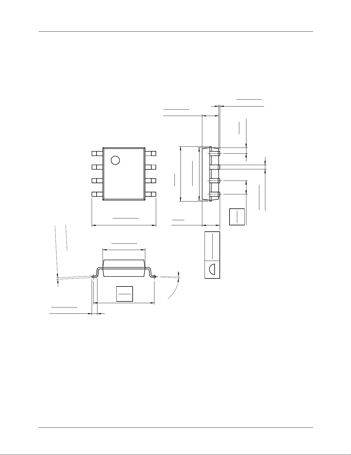
Mechanical Dimensions
Package
MC78LXXA/LM78LXXA/MC78L05AA
Dimensions in millimeters
0.46
±0.10
4.58
+0.25
–0.15
TO-92
±0.20
4.58
±0.40
14.47
1.27TYP
[1.27
±0.20
3.86MAX
±0.10
1.02
+0.10
–0.05
0.38
1.27TYP
]
±0.20
3.60
[1.27
±0.20
]
0.38
+0.10
–0.05
(0.25)
(R2.29)
10
Page 11
MC78LXXA/LM78LXXA/MC78L05AA
Mechanical Dimensions
Package
#1
#4
6.00 ±0.30
0.006
0.15
0.236 ±0.012
(Continued)
8-SOP
1.55 ±0.20
0.061 ±0.008
#8
#5
MAX
5.13
0.202
1.80
0.071
4.92 ±0.20
MAX
Dimensions in millimeters
0.1~0.25
MIN
0.004~0.001
0.56
0.022
()
0.194 ±0.008
0.41 ±0.10
1.27
0.050
0.016 ±0.004
+
-0.002
-0.05
0.004
0.50 ±0.20
0.020 ±0.008
+
0.10
3.95 ±0.20
0.156 ±0.008
5.72
0.225
0~8°
MAX0.10
MAX0.004
11
Page 12
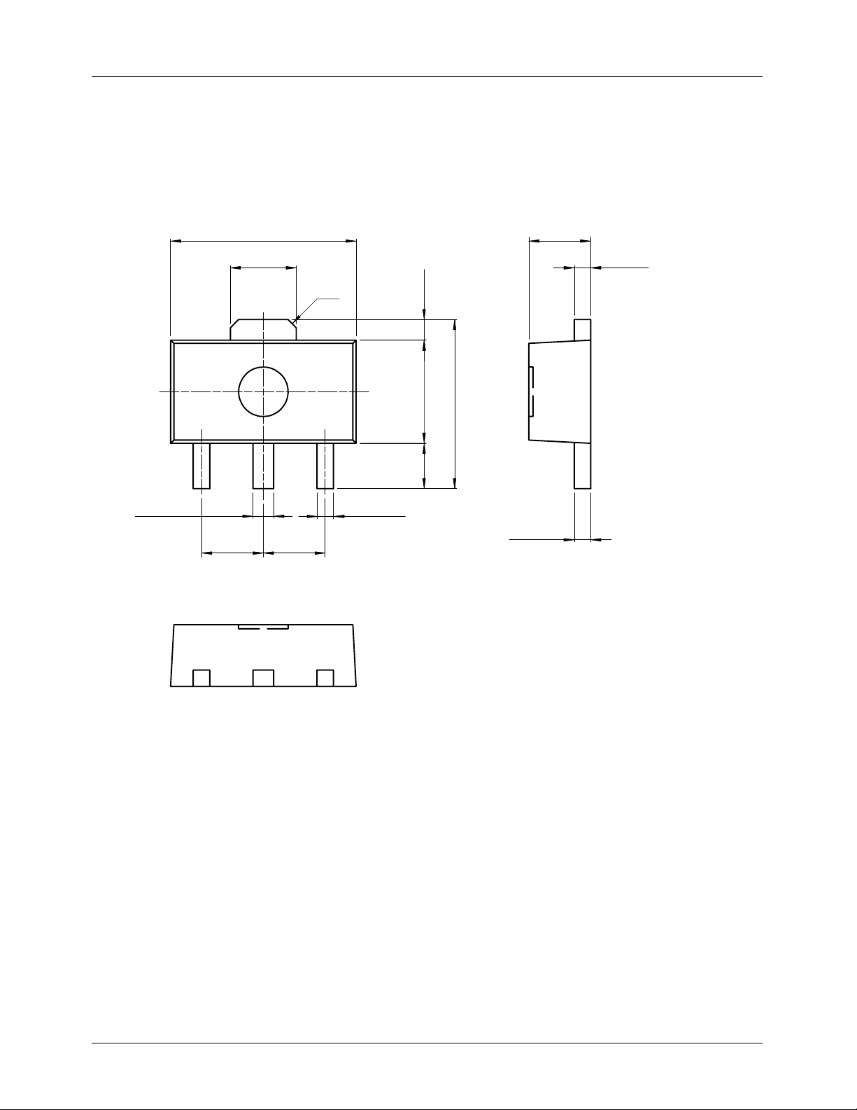
MC78LXXA/LM78LXXA/MC78L05AA
Mechanical Dimensions
Package
4.50
±0.20
1.65
±0.10
0.50
±0.10
1.50 TYP 1.50 TYP
(Continued)
SOT-89
C0.2
0.40
±0.10
(0.50)
±0.20
2.50
(1.10)
±0.20
4.10
Dimensions in millimeters
1.50
±0.20
(0.40)
+0.10
0.40
–0.05
12
Page 13

MC78LXXA/LM78LXXA/MC78L05AA
Ordering Information
Product Number Package Output Voltage Tolerance Operating Temperature
LM78L05ACZ
LM78L12ACZ
Product Number Package Output Voltage Tolerance Operating Temperature
MC78L05ACP
MC78L08ACP
MC78L12ACP
MC78L15ACP
MC78L18ACP
MC78L24ACP
MC78L05ACD
MC78L12ACD
MC78L05ACH
MC78L12ACH
MC78L05AACP TO-92 2%
TO-92 5% 0 ~ +125°C
TO-92
5%
0 ~ +125°C
8-SOPMC78L08ACD
SOT-89MC78L08ACH
13
Page 14

MC78LXXA/LM78LXXA/MC78L05AA
DISCLAIMER
FAIRCHILD SEMICONDUCTOR RESERVES THE RIGHT TO MAKE CHANGES WITHOUT FURT HER NOTICE TO ANY
PRODUCTS HEREI N TO IMPROVE RELIABILITY, FUNCTIO N OR DESIGN. FAIRCH IL D DOES NOT ASSUME ANY
LIABILITY ARISING OUT OF THE APPLICATION OR USE OF ANY PRODUCT OR CIRCUIT DESCRIBED HEREIN; NEITHER
DOES IT CONVEY ANY LICENSE UNDER IT S PATENT RIGHTS, NOR THE RIGHTS OF OTHE RS.
LIFE SUPPORT POL I CY
FAIRCHILD’S PR ODUCTS ARE NOT AUTH ORIZED FOR USE AS C RITICAL COMPONENT S IN LIFE SUPPORT DE VICES
OR SYSTEMS WITHOUT THE EXPRESS WRITTEN APPROVAL OF THE PRESIDENT OF FAIRCHILD SEMICONDUCTOR
CORPORATION. As used herein :
1. Life support devices or systems are devices or systems
which, (a) are intended for surgical implant into the body,
or (b) support or sustain life, and (c) whose failure to
perform when properly used in accordance with
2. A critical component in any component of a life support
device or sy stem whose fai lure to perform can be
reasonably expec ted to cause the failur e of the life support
device or system, or to affect its safety or effec t iv ene ss .
instructions for use provided in the labeling, can be
reasonably expected to result in a significant injury of the
user.
www.fairchildsemi.com
7/2/02 0.0m 001
2002 Fairchild Semiconductor Corporation
Stock#DSxxxxxxxx
 Loading...