

Page 1
MC78L00A Series,
NCV78L00A
100 mA Positive Voltage
Regulators
The MC78L00A Series of positive voltage regulators are
inexpensive, easy-to-use devices suitable for a multitude of
applications that require a regulated supply of up to 100 mA. Like
their higher powered MC7800 and MC78M00 Series cousins, these
regulators feature internal current limiting and thermal shutdown
making them remarkably rugged. No external components are
required with the MC78L00 devices in many applications.
These devices offer a substantial performance advantage over the
traditional zener diode-resistor combination, as output impedance
and quiescent current are substantially reduced.
Features
•Wide Range of Available, Fixed Output Voltages
•Low Cost
•Internal Short Circuit Current Limiting
•Internal Thermal Overload Protection
•No External Components Required
•Complementary Negative Regulators Offered (MC79L00A Series)
•Pb-Free Packages are Available
•NCV Prefix for Automotive and Other Applications Requiring Site
and Control Changes
3.0
Input
Output
15k
Q1
3.8k
Q3 Q5
Q4 Q6
Q11
Q12
Q10
5.0k
0-25k
http://onsemi.com
1
2
3
STRAIGHT LEAD
BULK PACK
TO-92
P SUFFIX
CASE 029
8
1
*SOIC-8 is an internally modified SO-8 package. Pins
2, 3, 6, and 7 are electrically common to the die attach
flag. This internal lead frame modification decreases
package thermal resistance and increases power
dissipation capability when appropriately mounted on
a printed circuit board. SOIC-8 conforms to all ex‐
ternal dimensions of the standard SO-8 package.
1
2
3
BENT LEAD
TAPE & REEL
AMMO PACK
Pin: 1. Output
2. Ground
3. Input
SOIC-8*
D SUFFIX
CASE 751
Q2
1.9k 19k 2.2k
C
Q8
Q7
1.0k
Q9
2.85k
Ground
1.2k
Z1
420
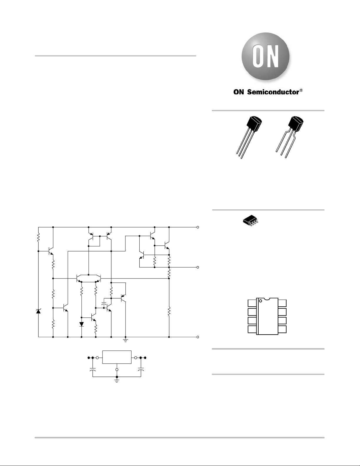
Figure 1. Representative Schematic Diagram
Input
Cin*
0.33mF
MC78LXXA
Output
CO**
Figure 2. Standard Application
A common ground is required between the input and the output voltages. The
input voltage must remain typically 2.0 V above the output voltage even during
the low point on the input ripple voltage.
* Cin is required if regulator is located an appreciable distance from power
supply filter.
** CO is not needed for stability; however, it does improve transient response.
© Semiconductor Components Industries, LLC, 2007
September, 2007 - Rev. 13
1 Publication Order Number:
PIN CONNECTIONS
18
V
OUT
2
GND
3
GND
4
NC
(Top View)
V
IN
7
GND
6
GND
5
NC
ORDERING INFORMATION
See detailed ordering and shipping information in the package
dimensions section on page 9 of this data sheet.
DEVICE MARKING INFORMATION
See general marking information in the device marking
section on page 15 of this data sheet.
MC78L00A/D
Page 2
MC78L00A Series, NCV78L00A
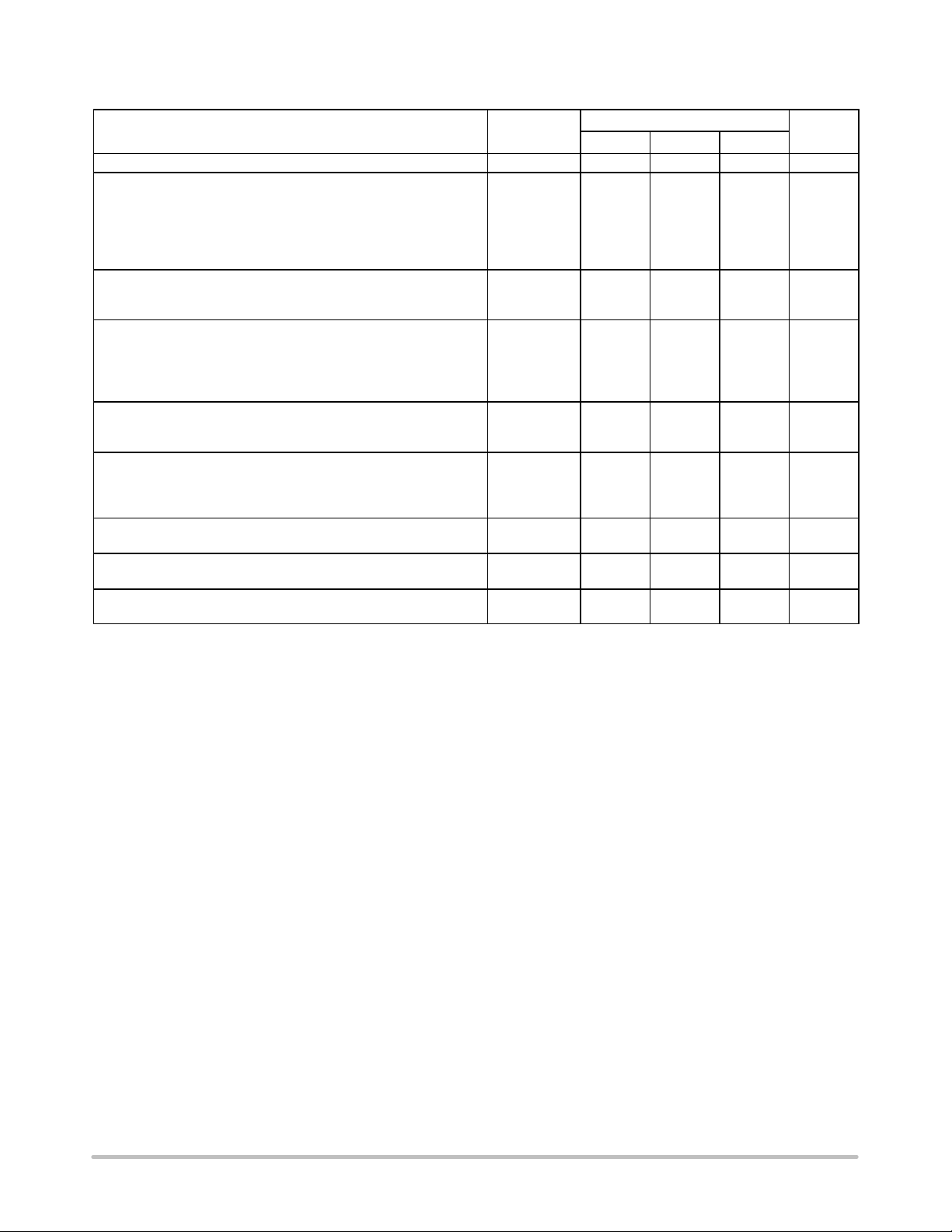
MAXIMUM RATINGS (T
= +125°C, unless otherwise noted.)
A
Rating Symbol Value Unit
Input Voltage (2.6 V-8.0 V)
Input Voltage (12 V-18 V)
Input Voltage (24 V)
Storage Temperature Range T
Operating Junction Temperature Range T
V
I
30
Vdc
35
40
stg
J
-65 to +150 °C
-40 to +150 °C
Stresses exceeding Maximum Ratings may damage the device. Maximum Ratings are stress ratings only. Functional operation above the
Recommended Operating Conditions is not implied. Extended exposure to stresses above the Recommended Operating Conditions may affect
device reliability.
*This device series contains ESD protection and exceeds the following tests:
Human Body Model 2000 V per MIL-STD-883, Method 3015
Machine Model Method 200 V
ELECTRICAL CHARACTERISTICS (V
= 10 V, IO = 40 mA, CI = 0.33 mF, CO = 0.1 mF, -40°C < TJ < +125°C (for MC78LXXAB,
I
NCV78L05A), 0°C < TJ < +125°C (for MC78LXXAC), unless otherwise noted.)
MC78L05AC, AB, NCV78L05A
Characteristics Symbol Min Typ Max Unit
Output Voltage (TJ = +25°C) V
Line Regulation
Reg
O
line
4.8 5.0 5.2 Vdc
mV
(TJ = +25°C, IO = 40 mA)
7.0 Vdc ≤ V
8.0 Vdc ≤ V
Load Regulation
(TJ = +25°C, 1.0 mA ≤ I
(TJ = +25°C, 1.0 mA ≤ I
Output Voltage
(7.0 Vdc ≤ V
(VI = 10 V, 1.0 mA ≤ I
Input Bias Current
(TJ = +25°C)
(TJ = +125°C)
Input Bias Current Change
(8.0 Vdc ≤ V
(1.0 mA ≤ I
Output Noise Voltage
≤ 20 Vdc
I
≤ 20 Vdc
I
≤ 100 mA)
O
≤ 40 mA)
O
≤ 20 Vdc, 1.0 mA ≤ I
I
≤ 20 Vdc)
I
≤ 40 mA)
O
≤ 70 mA)
O
≤ 40 mA)
O
Reg
DI
-
-
load
-
-
V
O
4.75
4.75
I
IB
-
-
IB
-
-
V
n
- 40 - mV
55
45
11
5.0
3.8
150
100
mV
60
30
Vdc
-
-
5.25
5.25
mA
6.0
-
5.5
mA
-
-
1.5
0.1
(TA = +25°C, 10 Hz ≤ f ≤ 100 kHz)
Ripple Rejection (IO = 40 mA,
f = 120 Hz, 8.0 Vdc ≤ V
≤ 18 V, TJ = +25°C)
I
Dropout Voltage (TJ = +25°C) V
NOTE: NCV78L05A: T
= -40°C, T
low
= +125°C. Guaranteed by design. NCV prefix is for automotive and other applications requiring
high
RR 41 49 - dB
I
- V
O
- 1.7 - Vdc
site and change control.
http://onsemi.com
2
Page 3
MC78L00A Series, NCV78L00A
ELECTRICAL CHARACTERISTICS (V
= 14 V, IO = 40 mA, CI = 0.33 mF, CO = 0.1 mF, -40°C < TJ < +125°C (for MC78LXXAB),
I
0°C < TJ < +125°C (for MC78LXXAC), unless otherwise noted.)
Characteristics Symbol Min Typ Max Unit
Output Voltage (TJ = +25°C) V
Line Regulation
(TJ = +25°C, IO = 40 mA)
10.5 Vdc ≤ V
11 Vdc ≤ V
≤ 23 Vdc
I
≤ 23 Vdc
I
Load Regulation
(TJ = +25°C, 1.0 mA ≤ I
(TJ = +25°C, 1.0 mA ≤ I
≤ 100 mA)
O
≤ 40 mA)
O
Output Voltage
(10.5 Vdc ≤ V
≤ 23 Vdc, 1.0 mA ≤ I
I
(VI = 14 V, 1.0 mA ≤ I
≤ 70 mA)
O
≤ 40 mA)
O
Input Bias Current
(TJ = +25°C)
(TJ = +125°C)
Input Bias Current Change
(11 Vdc ≤ V
(1.0 mA ≤ I
≤ 23 Vdc)
I
≤ 40 mA)
O
Output Noise Voltage
(TA = +25°C, 10 Hz ≤ f ≤ 100 kHz)
Ripple Rejection (IO = 40 mA,
f = 120 Hz, 12 V ≤ V
≤ 23 V, TJ = +25°C)
I
Dropout Voltage (TJ = +25°C) V
MC78L08AC, AB
7.7 8.0 8.3 Vdc
-
-
-
-
7.6
7.6
-
-
-
-
20
12
15
8.0
3.0
175
125
80
40
-
-
8.4
8.4
6.0
-
-
-
5.5
1.5
0.1
- 60 - mV
Reg
Reg
DI
O
line
load
V
O
I
IB
IB
V
n
RR 37 57 - dB
I
- V
O
- 1.7 - Vdc
mV
mV
Vdc
mA
mA
ELECTRICAL CHARACTERISTICS (V
= 15 V, IO = 40 mA, CI = 0.33 mF, CO = 0.1 mF, -40°C < TJ < +125°C (for MC78LXXAB),
I
0°C < TJ < +125°C (for MC78LXXAC), unless otherwise noted.)
Characteristics Symbol Min Typ Max Unit
Output Voltage (TJ = +25°C) V
Line Regulation
(TJ = +25°C, IO = 40 mA)
11.5 Vdc ≤ V
12 Vdc ≤ V
≤ 24 Vdc
I
≤ 24 Vdc
I
Load Regulation
(TJ = +25°C, 1.0 mA ≤ I
(TJ = +25°C, 1.0 mA ≤ I
≤ 100 mA)
O
≤ 40 mA)
O
Output Voltage
(11.5 Vdc ≤ V
≤ 24 Vdc, 1.0 mA ≤ I
I
(VI = 15 V, 1.0 mA ≤ I
≤ 70 mA)
O
≤ 40 mA)
O
Input Bias Current
(TJ = +25°C)
(TJ = +125°C)
Input Bias Current Change
(11 Vdc ≤ V
(1.0 mA ≤ I
≤ 23 Vdc)
I
≤ 40 mA)
O
Output Noise Voltage
(TA = +25°C, 10 Hz ≤ f ≤ 100 kHz)
Ripple Rejection (IO = 40 mA,
f = 120 Hz, 13 V ≤ V
≤ 24 V, TJ = +25°C)
I
Dropout Voltage
(TJ = +25°C)
MC78L09AC, AB
8.6 9.0 9.4 Vdc
-
-
-
-
8.5
8.5
-
-
-
-
20
12
15
8.0
3.0
175
125
90
40
-
-
9.5
9.5
6.0
-
-
-
5.5
1.5
0.1
- 60 - mV
Reg
Reg
DI
O
line
load
V
O
I
IB
IB
V
n
RR 37 57 - dB
V
I
- V
O
- 1.7 - Vdc
mV
mV
Vdc
mA
mA
http://onsemi.com
3
Page 4
MC78L00A Series, NCV78L00A
ELECTRICAL CHARACTERISTICS (V
= 19 V, IO = 40 mA, CI = 0.33 mF, CO = 0.1 mF, -40°C < TJ < +125°C (for MC78LXXAB),
I
0°C < TJ < +125°C (for MC78LXXAC), unless otherwise noted.)
Characteristics Symbol Min Typ Max Unit
Output Voltage (TJ = +25°C) V
Line Regulation
= +25°C, IO = 40 mA)
(T
J
14.5 Vdc ≤ V
16 Vdc ≤ V
≤ 27 Vdc
I
≤ 27 Vdc
I
Load Regulation
(TJ = +25°C, 1.0 mA ≤ I
(TJ = +25°C, 1.0 mA ≤ I
≤ 100 mA)
O
≤ 40 mA)
O
Output Voltage
(14.5 Vdc ≤ V
≤ 27 Vdc, 1.0 mA ≤ I
I
(VI = 19 V, 1.0 mA ≤ I
≤ 70 mA)
O
≤ 40 mA)
O
Input Bias Current
(TJ = +25°C)
(TJ = +125°C)
Input Bias Current Change
(16 Vdc ≤ V
(1.0 mA ≤ I
≤ 27 Vdc)
I
≤ 40 mA)
O
Output Noise Voltage
(TA = +25°C, 10 Hz ≤ f ≤ 100 kHz)
Ripple Rejection (IO = 40 mA,
f = 120 Hz, 15 V ≤ V
≤ 25 V, TJ = +25°C)
I
Dropout Voltage
(TJ = +25°C)
MC78L12AC, AB
11.5 12 12.5 Vdc
-
-
-
-
11.4
11.4
-
-
-
-
120
100
20
10
-
-
4.2
-
-
-
250
200
100
50
12.6
12.6
6.5
6.0
1.5
0.1
- 80 - mV
Reg
Reg
DI
O
line
load
V
O
I
IB
IB
V
n
RR 37 42 - dB
V
I
- V
O
- 1.7 - Vdc
mV
mV
Vdc
mA
mA
ELECTRICAL CHARACTERISTICS (V
S 0°C < T
< +125°C (for MC78LXXAC), unless otherwise noted.)
J
= 23 V, IO = 40 mA, CI = 0.33 mF, CO = 0.1 mF, -40°C < TJ < +125°C (for MC78LXXAB),
I
Characteristics Symbol Min Typ Max Unit
Output Voltage (TJ = +25°C) V
Line Regulation
(TJ = +25°C, IO = 40 mA)
17.5 Vdc ≤ V
20 Vdc ≤ V
≤ 30 Vdc
I
≤ 30 Vdc
I
Load Regulation
(TJ = +25°C, 1.0 mA ≤ I
(TJ = +25°C, 1.0 mA ≤ I
≤ 100 mA)
O
≤ 40 mA)
O
Output Voltage
(17.5 Vdc ≤ V
≤ 30 Vdc, 1.0 mA ≤ I
I
(VI = 23 V, 1.0 mA ≤ I
≤ 70 mA)
O
≤ 40 mA)
O
Input Bias Current
(TJ = +25°C)
(TJ = +125°C)
Input Bias Current Change
(20 Vdc ≤ V
(1.0 mA ≤ I
≤ 30 Vdc)
I
≤ 40 mA)
O
Output Noise Voltage
(TA = +25°C, 10 Hz ≤ f ≤ 100 kHz)
Ripple Rejection (IO = 40 mA,
f = 120 Hz, 18.5 V ≤ V
≤ 28.5 V, TJ = +25°C)
I
Dropout Voltage
(TJ = +25°C)
MC78L15AC, AB / NCV78L15A
14.4 15 15.6 Vdc
-
-
-
-
14.25
14.25
-
-
-
-
130
110
25
12
-
-
4.4
-
-
-
300
250
150
75
15.75
15.75
6.5
6.0
1.5
0.1
- 90 - mV
Reg
Reg
DI
O
line
load
V
O
I
IB
IB
V
n
RR 34 39 - dB
V
I
- V
O
- 1.7 - Vdc
mV
mV
Vdc
mA
mA
http://onsemi.com
4
Page 5
MC78L00A Series, NCV78L00A
ELECTRICAL CHARACTERISTICS (V
= 27 V, IO = 40 mA, CI = 0.33 mF, CO = 0.1 mF, 0 °C < TJ < +125°C, unless otherwise noted.)
I
Characteristics Symbol Min Typ Max Unit
Output Voltage (TJ = +25°C) V
Line Regulation
(TJ = +25°C, IO = 40 mA)
21.4 Vdc ≤ V
20.7 Vdc ≤ V
22 Vdc ≤ V
21 Vdc ≤ V
≤ 33 Vdc
I
≤ 33 Vdc
I
≤ 33 Vdc
I
≤ 33 Vdc
I
Load Regulation
(TJ = +25°C, 1.0 mA ≤ I
(TJ = +25°C, 1.0 mA ≤ I
≤ 100 mA)
O
≤ 40 mA)
O
Output Voltage
(21.4 Vdc ≤ V
(20.7 Vdc ≤ V
≤ 33 Vdc, 1.0 mA ≤ I
I
≤ 33 Vdc, 1.0 mA ≤ I
I
(VI = 27 V, 1.0 mA ≤ I
(VI = 27 V, 1.0 mA ≤ I
≤ 70 mA)
O
≤ 70 mA)
O
≤ 40 mA)
O
≤ 40 mA)
O
Input Bias Current
(TJ = +25°C)
(TJ = +125°C)
Input Bias Current Change
(22 Vdc ≤ V
(21 Vdc ≤ V
(1.0 mA ≤ I
≤ 33 Vdc)
I
≤ 33 Vdc)
I
≤ 40 mA)
O
Output Noise Voltage
(TA = +25°C, 10 Hz ≤ f ≤ 100 kHz)
Ripple Rejection (IO = 40 mA,
f = 120 Hz, 23 V ≤ V
≤ 33 V, TJ = +25°C)
I
Dropout Voltage
(TJ = +25°C)
MC78L18AC
17.3 18 18.7 Vdc
-
-
-
-
17.1
17.1
-
-
-
-
45
35
30
15
3.1
325
275
170
85
-
-
18.9
18.9
6.5
-
-
-
6.0
1.5
0.1
- 150 - mV
Reg
Reg
DI
O
line
load
V
O
I
IB
IB
V
n
RR 33 48 - dB
V
I
- V
O
- 1.7 - Vdc
mV
mV
Vdc
mA
mA
http://onsemi.com
5
Page 6

MC78L00A Series, NCV78L00A
ELECTRICAL CHARACTERISTICS (V
= 33 V, IO = 40 mA, CI = 0.33 mF, CO = 0.1 mF, 0 °C < TJ < +125°C, unless otherwise noted.)
I
Characteristics Symbol Min Typ Max Unit
Output Voltage (TJ = +25°C) V
Line Regulation
(TJ = +25°C, IO = 40 mA)
27.5 Vdc ≤ V
28 Vdc ≤ V
27 Vdc ≤ V
≤ 38 Vdc
I
≤ 80 Vdc
I
≤ 38 Vdc
I
Load Regulation
(TJ = +25°C, 1.0 mA ≤ I
(TJ = +25°C, 1.0 mA ≤ I
≤ 100 mA)
O
≤ 40 mA)
O
Output Voltage
(28 Vdc ≤ V
(27 Vdc ≤ V
(28 Vdc ≤ V
(27 Vdc ≤ V
≤ 38 Vdc, 1.0 mA ≤ I
I
≤ 38 Vdc, 1.0 mA ≤ I
I
33 Vdc, 1.0 mA ≤ I
I =
≤ 33 Vdc, 1.0 mA ≤ I
I
≤ 40 mA)
O
≤ 40 mA)
O
≤ 70 mA)
O
≤ 70 mA)
O
Input Bias Current
(TJ = +25°C)
(TJ = +125°C)
Input Bias Current Change
(28 Vdc ≤ V
(1.0 mA ≤ I
≤ 38 Vdc)
I
≤ 40 mA)
O
Output Noise Voltage
(TA = +25°C, 10 Hz ≤ f ≤ 100 kHz)
Ripple Rejection (IO = 40 mA,
f = 120 Hz, 29 V ≤ V
≤ 35 V, TJ = +25°C)
I
Dropout Voltage
(TJ = +25°C)
MC78L24AC
23 24 25 Vdc
-
-
-
-
-
22.8
22.8
-
-
-
-
50
60
40
20
3.1
-
300
350
200
100
-
-
25.2
25.2
6.5
-
-
-
6.0
1.5
0.1
- 200 - mV
Reg
Reg
DI
O
line
load
V
O
I
IB
IB
V
n
RR 31 45 - dB
V
I
- V
O
- 1.7 - Vdc
mV
mV
Vdc
mA
mA
http://onsemi.com
6
Page 7

MC78L00A Series, NCV78L00A
8.0
MC78L05AC
V
= 5.0 V
out
TJ = 25°C
6.0
4.0
, OUTPUT VOLTAGE (V)
O
2.0
0
0 2.0 4.0 6.0 8.0 10
IO = 40 mA
IO = 1.0 mA
IO = 100 mA
VI, INPUT VOLTAGE (V)
Figure 3. Dropout Characteristics Figure 4. Dropout Voltage versus
4.2
4.0
3.8
3.6
3.4
3.2
, INPUT BIAS CURRENT (mA) V
I
MC78L05AC
VI = 10 V
IB
VO= 5.0 V
3.0
IO = 40 mA
0
0 25 50 75 100 125
TA, AMBIENT TEMPERATURE (°C)
Figure 5. Input Bias Current versus
Ambient Temperature
2.5
2.0
1.5
1.0
0.5
0
, INPUT/OUTPUT DIFFERENTIAL VOLTAGE (V)
0 25 50 75 100 125
-VV
IO
IO = 40 mA
Dropout of Regulation is
defined as when
VO = 2% of V
TJ, JUNCTION TEMPERATURE (°C)
IO = 70 mA
IO = 1.0 mA
O
Junction Temperature
5.0
4.0
3.0
2.0
, INPUT BIAS CURRENT (mA)
IB
1.0
I
0
0 5.0 10 15 20 25 30 35 40
VI, INPUT VOLTAGE (V)
MC78L05AC
V
= 5.0 V
out
IO = 40 mA
TJ = 25°C
Figure 6. Input Bias Current
versus Input Voltage
10,000
1000
100
, POWER DISSIPATION (mW)
D
R
= 200°C/W
q
P
JA
P
to 25°C = 625 mW
D(max)
10
25 50 75 100 125 150
TA, AMBIENT TEMPERATURE (°C)
No Heatsink
Figure 7. Maximum Average Power Dissipation versus
Ambient Temperature - TO-92 Type Package
http://onsemi.com
170
150
130
110
JUNCTION‐TO‐AIR ( C/W)°
90
70
50
30
02030504010
JAθ
R , THERMAL RESISTANCE
R
q
JA
L, LENGTH OF COPPER (mm)
P
for TA = 50°C
D(max)
Graph represents symmetrical layout
2.0 oz.
L
Copper
Figure 8. SOIC-8 Thermal Resistance and Maximum
Power Dissipation versus P.C.B. Copper Length
7
3.2
2.8
2.4
2.0
1.6
3.0 mmL
1.2
0.8
0.4
, MAXIMUM POWER DISSIPATION (W)
D
P
Page 8
MC78L00A Series, NCV78L00A
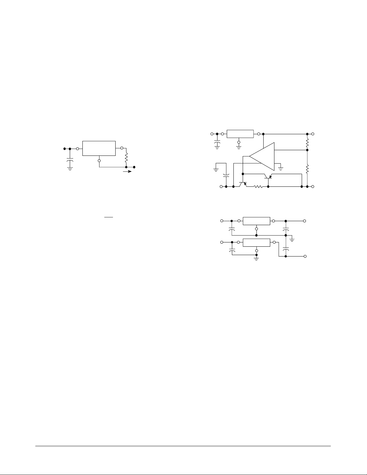
APPLICATIONS INFORMATION
Design Considerations
The MC78L00A Series of fixed voltage regulators are
designed with Thermal Overload Protection that shuts
down the circuit when subjected to an excessive power
overload condition. Internal Short Circuit Protection limits
the maximum current the circuit will pass.
In many low current applications, compensation
capacitors are not required. However, it is recommended
that the regulator input be bypassed with a capacitor if the
regulator is connected to the power supply filter with long
wire lengths, or if the output load capacitance is large. The
Input
0.33mF
The MC78L00 regulators can also be used as a current source
when connected as above. In order to minimize dissipation the
MC78L05C is chosen in this application. Resistor R determines
the current as follows:
IIB = 3.8 mA over line and load changes
For example, a 100 mA current source would require R to be a
50W, 1/2 W resistor and the output voltage compliance would be
the input voltage less 7 V.
MC78L05A
5.0 V
IO =
R
Constant
Current to
Grounded Load
I
O
+ I
B
R
input bypass capacitor should be selected to provide good
high-frequency characteristics to insure stable operation
under all load conditions. A 0.33 mF or larger tantalum,
mylar, or other capacitor having low internal impedance at
high frequencies should be chosen. The bypass capacitor
should be mounted with the shortest possible leads directly
across the regulators input terminals. Good construction
techniques should be used to minimize ground loops and
lead resistance drops since the regulator has no external
sense lead. Bypassing the output is also recommended.
+20V
0.33mF
0.33mF
20V
Figure 10. ± 15 V Tracking Voltage Regulator
MC78L15A +V
7
2
MC1741
4
6.5
-
3
+
MPS A70
+V
I
0.33mF
-V
I
0.33mF
6
MPS U55
MC78LXXA
MC79LXXA
0.1mF
0.1mF
+V
O
10k
10k
-V
O
O
-V
O
Figure 9. Current Regulator
Figure 11. Positive and Negative Regulator
http://onsemi.com
8
Page 9
MC78L00A Series, NCV78L00A
ORDERING INFORMATION
Operating
Device Output Voltage
MC78L05ABD
MC78L05ABDG SOIC-8 98 Units/Rail
MC78L05ABDR2 SOIC-8 2500 Tape & Reel
MC78L05ABDR2G SOIC-8 (Pb-Free) 2500 Tape & Reel
NCV78L05ABDR2* SOIC-8 2500 Tape & Reel
NCV78L05ABDR2G* SOIC-8 (Pb-Free) 2500 Tape & Reel
MC78L05ABP TO-92 2000 Units/Bag
MC78L05ABPG TO-92 (Pb-Free) 2000 Units/Bag
NCV78L05ABPG* TO-92 (Pb-Free) 2000 Units/Bag
MC78L05ABPRA TO-92 2000 Tape & Reel
MC78L05ABPRAG TO-92 (Pb-Free) 2000 Tape & Reel
NCV78L05ABPRAG* TO-92 (Pb-Free) 2000 Tape & Reel
MC78L05ABPRE TO-92 2000 Tape & Reel
MC78L05ABPREG TO-92 (Pb-Free) 2000 Tape & Reel
NCV78L05ABPREG* TO-92 (Pb-Free) 2000 Tape & Reel
MC78L05ABPRM TO-92 2000 Ammo Pack
MC78L05ABPRMG TO-92 (Pb-Free) 2000 Ammo Pack
NCV78L05ABPRMG* TO-92 (Pb-Free) 2000 Ammo Pack
NCV78L05ABPRPG* TO-92 (Pb-Free) 2000 Ammo Pack
MC78L05ACD
MC78L05ACDG SOIC-8 (Pb-Free) 98 Units/Rail
MC78L05ACDR2 SOIC-8 2500 Tape & Reel
MC78L05ACDR2G SOIC-8 (Pb-Free) 2500 Tape & Reel
MC78L05ACP TO-92 2000 Units/Bag
MC78L05ACPG TO-92 (Pb-Free) 2000 Units/Bag
MC78L05ACPRA TO-92 2000 Tape & Reel
MC78L05ACPRAG TO-92 (Pb-Free) 2000 Tape & Reel
MC78L05ACPRE TO-92 2000 Tape & Reel
MC78L05ACPREG TO-92 (Pb-Free) 2000 Tape & Reel
MC78L05ACPRM TO-92 2000 Ammo Pack
MC78L05ACPRMG TO-92 (Pb-Free) 2000 Ammo Pack
MC78L05ACPRP TO-92 2000 Ammo Pack
MC78L05ACPRPG TO-92 (Pb-Free) 2000 Ammo Pack
*NCV78L05A: T
†For information on tape and reel specifications, including part orientation and tape sizes, please refer to our Tape and Reel Packaging
Specifications Brochure, BRD8011/D.
= -40°C, T
low
= +125°C. Guaranteed by design. NCV prefix is for automotive and other applications requiring site and change control.
high
5.0 V TJ = -40° to +125°C
5.0 V TJ = 0° to +125°C
Temperature Range
Package Shipping
SOIC-8 98 Units/Rail
SOIC-8 98 Units/Rail
†
http://onsemi.com
9
Page 10

ORDERING INFORMATION (continued)
Device Output Voltage
MC78L08ABD
MC78L08ABDG
MC78L08ABDR2
MC78L08ABDR2G
NCV78L08ABDR2*
NCV78L08ABDR2G*
MC78L08ABP
MC78L08ABPG
MC78L08ABPRA
MC78L08ABPRAG
MC78L08ABPRP
MC78L08ABPRPG
MC78L08ACD
MC78L08ACDG
MC78L08ACDR2
MC78L08ACDR2G
MC78L08ACP
MC78L08ACPG
MC78L08ACPRA
MC78L08ACPRAG
MC78L08ACPRE
MC78L08ACPREG
MC78L08ACPRP
MC78L08ACPRPG
MC78L00A Series, NCV78L00A
Operating
Temperature Range
TJ = -40° to +125°C
8.0 V
TJ = 0° to +125°C
Package Shipping
SOIC-8
SOIC-8
(Pb-Free)
SOIC-8
SOIC-8
(Pb-Free)
SOIC-8
SOIC-8
(Pb-Free)
TO-92
TO-92
(Pb-Free)
TO-92
TO-92
(Pb-Free)
TO-92
TO-92
(Pb-Free)
SOIC-8
SOIC-8
(Pb-Free)
SOIC-8
SOIC-8
(Pb-Free)
TO-92
TO-92
(Pb-Free)
TO-92
TO-92
(Pb-Free)
TO-92
TO-92
(Pb-Free)
TO-92
TO-92
(Pb-Free)
98 Units/Rail
98 Units/Rail
2500 Tape & Reel
2500 Tape & Reel
2500 Tape & Reel
2500 Tape & Reel
2000 Units/Bag
2000 Units/Bag
2000 Tape & Reel
2000 Tape & Reel
2000 Ammo Pack
2000 Ammo Pack
98 Units/Rail
98 Units/Rail
2500 Tape & Reel
2500 Tape & Reel
2000 Units/Bag
2000 Units/Bag
2000 Tape & Reel
2000 Tape & Reel
2000 Tape & Reel
2000 Tape & Reel
2000 Ammo Pack
2000 Ammo Pack
†
http://onsemi.com
10
Page 11

MC78L00A Series, NCV78L00A
ORDERING INFORMATION (continued)(continued)
Operating
Device Shipping
MC78L09ABD
MC78L09ABDG
MC78L09ABDR2
MC78L09ABDR2G
MC78L09ABPRA
MC78L09ABPRAG
MC78L09ABPRP
MC78L09ABPRPG
MC78L09ACD
MC78L09ACDG
MC78L09ACDR2
MC78L09ACDR2G
MC78L09ACP
MC78L09ACPG
†For information on tape and reel specifications, including part orientation and tape sizes, please refer to our Tape and Reel Packaging
Specifications Brochure, BRD8011/D.
Output Voltage
9.0 V TJ = -40° to +125°C
9.0 V TJ = 0° to +125°C
Temperature Range
Package
SOIC-8
SOIC-8
(Pb-Free)
SOIC-8
SOIC-8
(Pb-Free)
TO-92
TO-92
(Pb-Free)
TO-92
TO-92
(Pb-Free)
SOIC-8
SOIC-8
(Pb-Free)
SOIC-8
SOIC-8
(Pb-Free)
TO-92
TO-92
(Pb-Free)
98 Units/Rail
98 Units/Rail
2500 Tape & Reel
2500 Tape & Reel
2000 Tape & Reel
2000 Tape & Reel
2000 Ammo Pack
2000 Ammo Pack
98 Units/Rail
98 Units/Rail
2500 Tape & Reel
2500 Tape & Reel
2000 Units/Bag
2000 Units/Bag
†
http://onsemi.com
11
Page 12

MC78L00A Series, NCV78L00A
ORDERING INFORMATION (continued)
Operating
Device Output Voltage
MC78L12ABD
MC78L12ABDG
MC78L12ABDR2
MC78L12ABDR2G
NCV78L12ABDG*
NCV78L12ABDR2* SOIC-8 2500 Tape & Reel
NCV78L12ABDR2G* SOIC-8
MC78L12ABP
MC78L12ABPG
MC78L12ABPRP
MC78L12ABPRPG
NCV78L12ABPG*
MC78L12ACD
MC78L12ACDG
MC78L12ACDR2
MC78L12ACDR2G
MC78L12ACP
MC78L12ACPG
MC78L12ACPRA
MC78L12ACPRAG TO-92
MC78L12ACPRE
MC78L12ACPREG
MC78L12ACPRM
MC78L12ACPRMG TO-92
MC78L12ACPRP
MC78L12ACPRPG
*NCV78L12A: T
†For information on tape and reel specifications, including part orientation and tape sizes, please refer to our Tape and Reel Packaging
Specifications Brochure, BRD8011/D.
= -40°C, T
low
= +125°C. Guaranteed by design. NCV prefix is for automotive and other applications requiring site and change control.
high
12 V
Temperature Range
TJ = -40° to +125°C
TJ = 0° to +125°C
Package Shipping
SOIC-8
SOIC-8
(Pb-Free)
SOIC-8
SOIC-8
(Pb-Free)
SOIC-8
(Pb-Free)
(Pb-Free)
TO-92
TO-92
(Pb-Free)
TO-92
TO-92
(Pb-Free)
TO-92
(Pb-Free)
SOIC-8
SOIC-8
(Pb-Free)
SOIC-8
SOIC-8
(Pb-Free)
TO-92
TO-92
(Pb-Free)
TO-92
(Pb-Free)
TO-92
TO-92
(Pb-Free)
TO-92
(Pb-Free)
TO-92
TO-92
(Pb-Free)
98 Units/Rail
98 Units/Rail
2500 Tape & Reel
2500 Tape & Reel
98 Units/Rail
2500 Tape & Reel
2000 Units/Bag
2000 Units/Bag
2000 Ammo Pack
2000 Ammo Pack
2000 Units/Bag
98 Units/Rail
98 Units/Rail
2500 Tape & Reel
2500 Tape & Reel
2000 Units/Bag
2000 Units/Bag
2000 Tape & Reel
2000 Tape & Reel
2000 Tape & Reel
2000 Tape & Reel
2000 Ammo Pack
2000 Ammo Pack
2000 Ammo Pack
2000 Ammo Pack
†
http://onsemi.com
12
Page 13

MC78L00A Series, NCV78L00A
ORDERING INFORMATION (continued)
Operating
Device Output Voltage
MC78L15ABD
MC78L15ABDG SOIC-8
MC78L15ABDR2 SOIC-8 2500 Tape & Reel
MC78L15ABDR2G SOIC-8
NCV78L15ABDR2G* SOIC-8
MC78L15ABP TO-92 2000 Units/Bag
MC78L15ABPG TO-92
MC78L15ABPRA TO-92 2000 Tape & Reel
MC78L15ABPRAG TO-92
MC78L15ABPRP TO-92 2000 Ammo Pack
MC78L15ABPRPG TO-92
MC78L15ACD
MC78L15ACDG SOIC-8
MC78L15ACDR2 SOIC-8 2500 Tape & Reel
MC78L15ACDR2G SOIC-8
MC78L15ACP TO-92 2000 Units/Bag
MC78L15ACPG TO-92
MC78L15ACPRA TO-92 2000 Tape & Reel
MC78L15ACPRAG TO-92
MC78L15ACPRP TO-92 2000 Ammo Pack
MC78L15ACPRPG TO-92
*NCV78L15A: T
†For information on tape and reel specifications, including part orientation and tape sizes, please refer to our Tape and Reel Packaging
Specifications Brochure, BRD8011/D.
= -40°C, T
low
= +125°C. Guaranteed by design. NCV prefix is for automotive and other applications requiring site and change control.
high
15 V
Temperature Range
TJ = -40° to +125°C
TJ = 0° to +125°C
Package Shipping
SOIC-8 98 Units/Rail
98 Units/Rail
(Pb-Free)
2500 Tape & Reel
(Pb-Free)
2500 Tape & Reel
(Pb-Free)
2000 Units/Bag
(Pb-Free)
2000 Tape & Reel
(Pb-Free)
2000 Ammo Pack
(Pb-Free)
SOIC-8 98 Units/Rail
98 Units/Rail
(Pb-Free)
2500 Tape & Reel
(Pb-Free)
2000 Units/Bag
(Pb-Free)
2000 Tape & Reel
(Pb-Free)
2000 Ammo Pack
(Pb-Free)
†
http://onsemi.com
13
Page 14
MC78L00A Series, NCV78L00A
ORDERING INFORMATION (continued)
Operating
Device Output Voltage
MC78L18ABP
MC78L18ABPG TO-92
MC78L18ACP
MC78L18ACPG TO-92
MC78L18ACPRA TO-92 2000 Tape & Reel
MC78L18ACPRAG TO-92
MC78L18ACPRM TO-92 2000 Ammo Pack
MC78L18ACPRMG TO-92
MC78L18ACPRP TO-92 2000 Ammo Pack
MC78L18ACPRPG TO-92
MC78L24ABP
MC78L24ABPG TO-92
NCV78L24ABPRPG* TO-92
MC78L24ACP
MC78L24ACPG TO-92
MC78L24ACPRA TO-92 2000 Tape & Reel
MC78L24ACPRAG TO-92
MC78L24ACPRP TO-92 2000 Ammo Pack
MC78L24ACPRPG TO-92
†For information on tape and reel specifications, including part orientation and tape sizes, please refer to our Tape and Reel Packaging
Specifications Brochure, BRD8011/D.
18 V
24 V
Temperature Range
TJ = -40° to +125°C
TJ = 0° to +125°C
TJ = -40° to +125°C
TJ = 0° to +125°C
Package Shipping
TO-92 2000 Units/Bag
2000 Units/Bag
(Pb-Free)
TO-92 2000 Units/Bag
2000 Units/Bag
(Pb-Free)
2000 Tape & Reel
(Pb-Free)
2000 Ammo Pack
(Pb-Free)
2000 Ammo Pack
(Pb-Free)
TO-92 2000 Units/Bag
2000 Units/Bag
(Pb-Free)
2000 Units/Bag
(Pb-Free)
TO-92 2000 Units/Bag
2000 Units/Bag
(Pb-Free)
2000 Tape & Reel
(Pb-Free)
2000 Ammo Pack
(Pb-Free)
†
http://onsemi.com
14
Page 15

MC78L00A Series, NCV78L00A
MARKING DIAGRAMS
SOIC-8
D SUFFIX
CASE 751
8
8LxxA
ALYWB
G
1
xx = 05, 08, 09, 12, or 15
A = Assembly Location
L = Wafer Lot
Y = Year
W = Work Week
B, C = Temperature Range
G = Pb-Free Package
P SUFFIX
CASE 029
MC78L
zzABP
ALYWWG
G
8
1
TO-92
MC78L
zzACP
ALYWWG
8LxxA
ALYWC
G
G
123
zz = 05, 08, 09, 12, 15, 18 or 24
A = Assembly Location
L = Wafer Lot
Y = Year
WW = Work Week
G = Pb-Free Package
(Note: Microdot may be in either location)
123
http://onsemi.com
15
Page 16

-Y-
-Z-
MC78L00A Series, NCV78L00A
PACKAGE DIMENSIONS
SOIC-8 NB
D SUFFIX
CASE 751-07
ISSUE AJ
NOTES:
-XA
58
B
1
S
0.25 (0.010)
4
M
M
Y
K
G
N
C
SEATING
PLANE
0.10 (0.004)
H
D
0.25 (0.010) Z
M
Y
SXS
X 45
_
M
J
1. DIMENSIONING AND TOLERANCING PER
ANSI Y14.5M, 1982.
2. CONTROLLING DIMENSION: MILLIMETER.
3. DIMENSION A AND B DO NOT INCLUDE
MOLD PROTRUSION.
4. MAXIMUM MOLD PROTRUSION 0.15 (0.006)
PER SIDE.
5. DIMENSION D DOES NOT INCLUDE DAMBAR
PROTRUSION. ALLOWABLE DAMBAR
PROTRUSION SHALL BE 0.127 (0.005) TOTAL
IN EXCESS OF THE D DIMENSION AT
MAXIMUM MATERIAL CONDITION.
6. 751-01 THRU 751-06 ARE OBSOLETE. NEW
STANDARD IS 751-07.
MILLIMETERS
DIMAMIN MAX MIN MAX
4.80 5.00 0.189 0.197
B 3.80 4.00 0.150 0.157
C 1.35 1.75 0.053 0.069
D 0.33 0.51 0.013 0.020
G 1.27 BSC 0.050 BSC
H 0.10 0.25 0.004 0.010
J 0.19 0.25 0.007 0.010
K 0.40 1.27 0.016 0.050
M 0 8 0 8
____
N 0.25 0.50 0.010 0.020
S 5.80 6.20 0.228 0.244
INCHES
SOLDERING FOOTPRINT*
1.52
0.060
7.0
0.275
0.6
0.024
*For additional information on our Pb-Free strategy and soldering
details, please download the ON Semiconductor Soldering and
Mounting Techniques Reference Manual, SOLDERRM/D.
4.0
0.155
1.270
0.050
SCALE 6:1
ǒ
inches
mm
Ǔ
http://onsemi.com
16
Page 17

MC78L00A Series, NCV78L00A
PACKAGE DIMENSIONS
TO-92 (TO-226)
P SUFFIX
CASE 29-11
ISSUE AM
SEATING
PLANE
R
T
SEATING
PLANE
A
B
STRAIGHT LEAD
BULK PACK
R
P
L
K
XX
H
V
1
G
C
N
D
J
SECTION X-X
NOTES:
1. DIMENSIONING AND TOLERANCING PER ANSI
Y14.5M, 1982.
2. CONTROLLING DIMENSION: INCH.
3. CONTOUR OF PACKAGE BEYOND DIMENSION R
IS UNCONTROLLED.
4. LEAD DIMENSION IS UNCONTROLLED IN P AND
BEYOND DIMENSION K MINIMUM.
DIM MIN MAX MIN MAX
A 0.175 0.205 4.45 5.20
B 0.170 0.210 4.32 5.33
C 0.125 0.165 3.18 4.19
D 0.016 0.021 0.407 0.533
G 0.045 0.055 1.15 1.39
H 0.095 0.105 2.42 2.66
J 0.015 0.020 0.39 0.50
K 0.500 --- 12.70 ---
L 0.250 --- 6.35 ---
N 0.080 0.105 2.04 2.66
P --- 0.100 --- 2.54
R 0.115 --- 2.93 ---
V 0.135 --- 3.43 ---
MILLIMETERSINCHES
N
A
B
BENT LEAD
TAPE & REEL
AMMO PACK
P
K
XX
G
D
J
V
1
C
SECTION X-X
N
NOTES:
1. DIMENSIONING AND TOLERANCING PER
ASME Y14.5M, 1994.
2. CONTROLLING DIMENSION:
MILLIMETERS.
3. CONTOUR OF PACKAGE BEYOND
DIMENSION R IS UNCONTROLLED.
4. LEAD DIMENSION IS UNCONTROLLED IN
P AND BEYOND DIMENSION K MINIMUM.
MILLIMETERS
DIM MIN MAX
A 4.45 5.20
B 4.32 5.33
C 3.18 4.19
D 0.40 0.54
G 2.40 2.80
J 0.39 0.50
K 12.70 ---
N 2.04 2.66
P 1.50 4.00
R 2.93 ---
V 3.43 ---
ON Semiconductor and are registered trademarks of Semiconductor Components Industries, LLC (SCILLC). SCILLC reserves the right to make changes without further notice
to any products herein. SCILLC makes no warranty, representation or guarantee regarding the suitability of its products for any particular purpose, nor does SCILLC assume any
liability arising out of the application or use of any product or circuit, and specifically disclaims any and all liability, including without limitation special, consequential or incidental
damages. “Typical” parameters which may be provided in SCILLC data sheets and/or specifications can and do vary in different applications and actual performance may vary over
time. All operating parameters, including “Typicals” must be validated for each customer application by customer's technical experts. SCILLC does not convey any license under
its patent rights nor the rights of others. SCILLC products are not designed, intended, or authorized for use as components in systems intended for surgical implant into the body,
or other applications intended to support or sustain life, or for any other application in which the failure of the SCILLC product could create a situation where personal injury or death
may occur. Should Buyer purchase or use SCILLC products for any such unintended or unauthorized application, Buyer shall indemnify and hold SCILLC and its officers, employees,
subsidiaries, affiliates, and distributors harmless against all claims, costs, damages, and expenses, and reasonable attorney fees arising out of, directly or indirectly, any claim of
personal injury or death associated with such unintended or unauthorized use, even if such claim alleges that SCILLC was negligent regarding the design or manufacture of the part.
SCILLC is an Equal Opportunity/Affirmative Action Employer. This literature is subject to all applicable copyright laws and is not for resale in any manner.
PUBLICATION ORDERING INFORMATION
LITERATURE FULFILLMENT:
Literature Distribution Center for ON Semiconductor
P.O. Box 5163, Denver, Colorado 80217 USA
Phone: 303-675-2175 or 800-344-3860 Toll Free USA/Canada
Fax: 303-675-2176 or 800-344-3867 Toll Free USA/Canada
Email: orderlit@onsemi.com
N. American Technical Support: 800-282-9855 Toll Free
USA/Canada
Europe, Middle East and Africa Technical Support:
Phone: 421 33 790 2910
Japan Customer Focus Center
Phone: 81-3-5773-3850
http://onsemi.com
ON Semiconductor Website: www.onsemi.com
Order Literature: http://www.onsemi.com/orderlit
For additional information, please contact your loca
Sales Representative
MC78L00A/D
17
 Loading...