

Page 1
MC7660
Charge Pump DC-to-DC
V oltage Converter
The MC7660 is a pin–compatible replacement for the Industry
standard ICL7660 charge pump voltage converter . It converts a +1.5V
to +10V input to a corresponding –1.5V to –10V output using only two
low–cost capacitors, eliminating inductors and their associated cost,
size and EMI.
The on–board oscillator operates at a nominal frequency of 10kHz.
Operation below 10kHz (for lower supply current applications) is
possible by connecting an external capacitor from OSC to ground
(with pin 1 open).
The MC7660 is available in an 8–pin SOIC package in extended
temperature range.
Features
• Converts +5V Supply to –5V Supply
• Wide Input Voltage Range: 1.5V to 10V
• Ef ficient Voltage Conversion: 99.9%
• Excellent Power Efficiency: 98%
• Low Power Supply: 80µA @ 5V
• Low Cost and Easy to Use
– Only Two External Capacitors Required
• Available in Small Outline (SO) Package
• ESD Protection: ≥ 2.5kV
• No Dx Diode Required for High Voltage Operation
Typical Applications
• RS–232 Negative Bias
• Display Bias
• Data Aquisition Negative Supply Generation
IN
http://onsemi.com
SO–8
D SUFFIX
CASE 751
PIN CONFIGURATION
(Top View)
+
V
NC
1
+
2
CAP
3
GND
–
4
CAP
ORDERING INFORMATION
Device Package Shipping
MC7660DR2 8–Pin SOIC 2500 Tape/Reel
8
7
OSC
6
LV
5
V
OUT
OSC
LV
7
6
RC
OSCILLATOR
INTERNAL
REGULATOR
MC7660
Semiconductor Components Industries, LLC, 1999
February , 2000 – Rev. 2
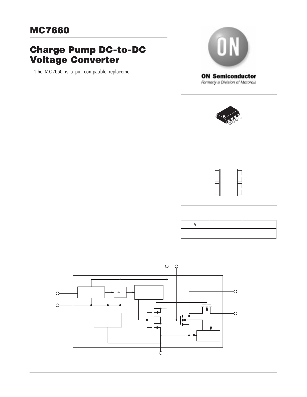
VOLTAGE
FUNCTIONAL BLOCK DIAGRAM
V+ CAP+
28
VOLTAGE–
B
2
LEVEL
TRANSLATOR
3
GND
1 Publication Order Number:
LOGIC
NETWORK
4
CAP–
5
V
OUT
MC7660/D
Page 2
MC7660
ABSOLUTE MAXIMUM RATINGS*
Parameter Value Unit
Supply Voltage +10.5 V
LV and OSC Inputs Voltage (Note 1.)
V+ < 5.5V
V+ > 5.5V
Current Into LV (Note 1.) V+ > 3.5V
Output Short Duration (V
SUPPLY
≤ 5.5V) Continuous
Power Dissipation (TA ≤ 70°C)
Derate above 50°C
–0.3 to (V+ + 0.3)
(V+ – 5.5) to (V+ + 0.3)
20 µA
470
5.5
Operating Temperature Range
–40 to +85
Storage Temperature Range –65 to +150 °C
Lead Temperature (Soldering, 10 Seconds) +300 °C
* Maximum Ratings are those values beyond which damage to the device may occur.
1. Connecting any input terminal to voltages greater than V+ or less than GND may cause destructive latch–up. It is recommended that no inputs
from sources operating from external supplies be applied prior to ”power up” of the MC7660.
V
mW
mW/°C
°C
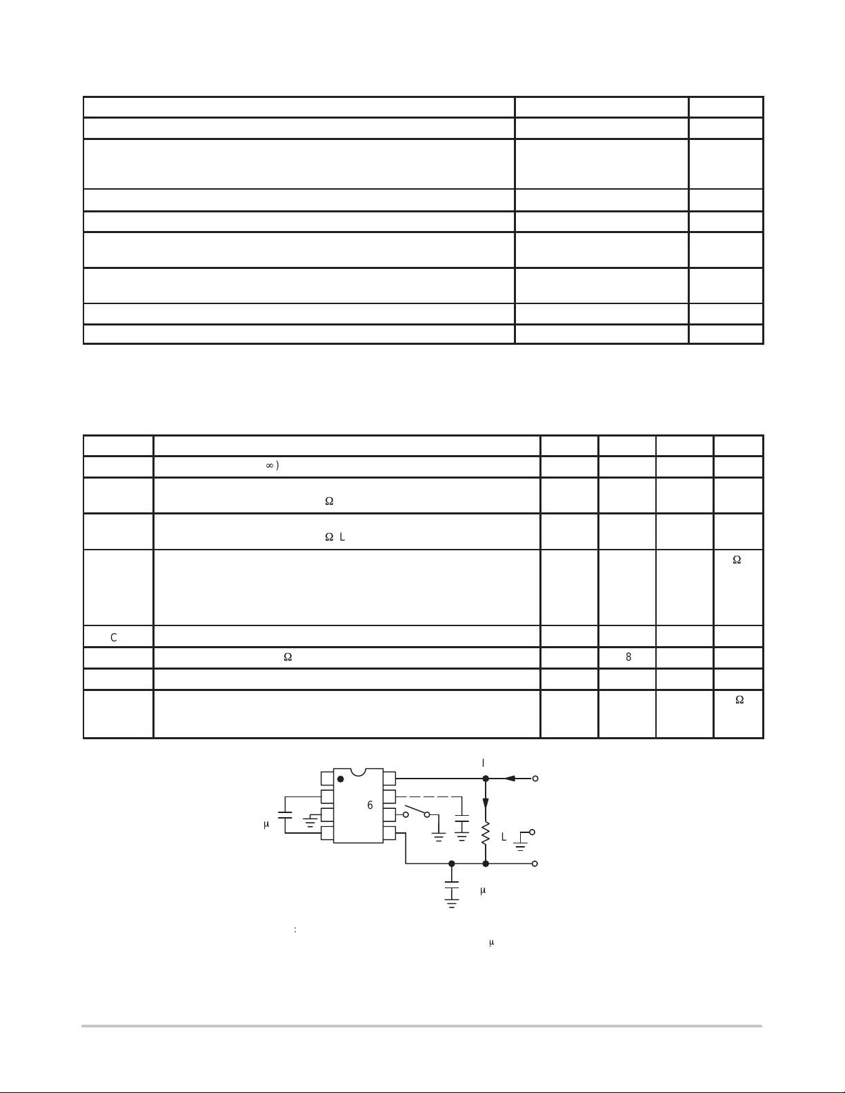
ELECTRICAL CHARACTERISTICS (Specifications Measured Over Operating Temperature Range, V+ = 5V, C
Test Circuit
(Figure 1), unless otherwise noted.
OSC
Symbol Characteristic Min Typ Max Unit
+
I
+
V
H
+
V
L
R
OUT
F
OSC
P
EFF
V
OUT EFF
Z
OSC
Supply Current (RL = R) — 80 180 µA
Supply Voltage Range, High
(–40°C ≤ TA ≤ +85°C, RL = 10 kW, LV Open)
3.0 — 10
Supply Voltage Range, Low
(–40°C ≤ TA ≤ +85°C, RL = 10 kW, LV to GND)
1.5 — 3.5
Output Source Resistance
I
= 20mA, TA = 25°C
OUT
I
= 20mA, 0°C ≤ TA ≤ +70°C
OUT
I
= 20mA, –40°C ≤ TA ≤ +85°C
OUT
V+ =2V, I
= 3 mA, LV to GND, 0°C ≤ TA ≤ +70°C
OUT
—
—
—
—
70
—
—
150
100
120
130
300
Oscillator Frequency (Pin 7 Open) — 10 — kHz
Power Efficiency (RL = 5kW)
95 98 — %
Voltage Conversion Efficiency 97 99.9 — %
Oscillator Impedance
V+ = 2V
V+ = 5V
C1
10 mF
—
—
I
1
2
+
MC7660
3
4
8
7
C
6
5
OSC
S
V+
I
L
R
L
(+6 V)
V
O
*
1000
100
—
—
= 0,
V
V
W
k
W
*NOTE: For large values of C
of C1 and C2 should be increased to 100 mF.
Figure 1. MC7660 T est Circuit
http://onsemi.com
C2
10 mF
+
(>1000 pF), the values
OSC
2
Page 3
MC7660
APPLICATIONS INFORMATION
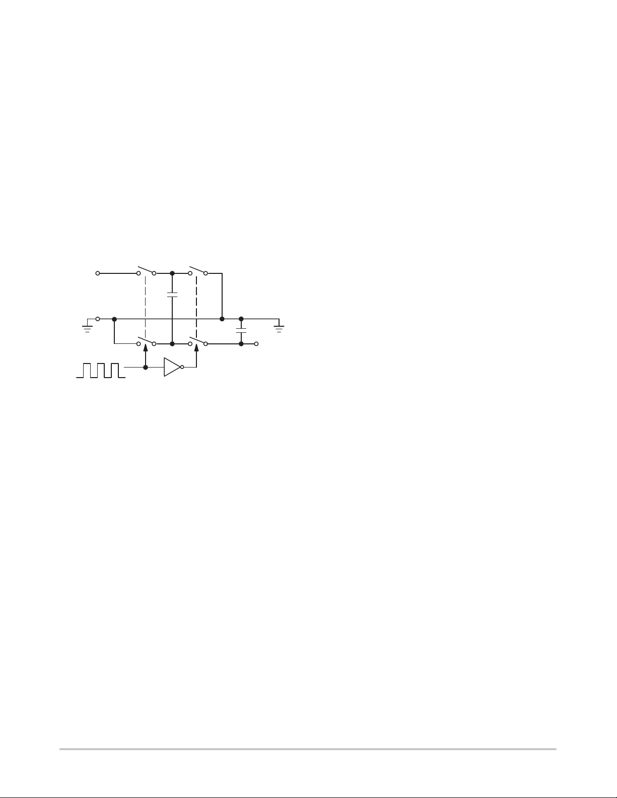
Detailed Description
The MC7660 contains all the necessary circuitry to
implement a voltage inverter, with the exception of two
external capacitors, which may be inexpensive 10 µF
polarized electrolytic capacitors. Operation is best
understood by considering Figure 2, which shows an
idealized voltage inverter. Capacitor C
voltage, V
+
, for the half cycle when switches S1 and S3 are
is charged to a
1
closed. (Note: Switches S2 and S4 are open during this half
cycle.) During the second half cycle of operation, switches
S2 and S4 are closed, with S1 and S3 open, thereby shifting
capacitor C1 negatively by V+ volts. Charge is then
transferred from C
to C2, such that the voltage on C2 is
1
exactly V+, assuming ideal switches and no load on C2.
V+
GND
Figure 2. Idealized Charge Pump Inverter
S1 S2
S3 S4
C1
C2
V
–V
OUT
IN
=
The four switches in Figure 2 are MOS power switches;
S
is a P–channel device, and S2, S3 and S4 are N–channel
1
devices. The main difficulty with this approach is that in
integrating the switches, the substrates of S3 and S4 must
always remain reverse–biased with respect to their sources,
but not so much as to degrade their ON resistances. In
addition, at circuit start–up, and under output short circuit
conditions (V
= V+), the output voltage must be sensed
OUT
and the substrate bias adjusted accordingly. Failure to
accomplish this will result in high power losses and probable
device latch–up.
This problem is eliminated in the MC7660 by a logic
network which senses the output voltage (V
) together
OUT
with the level translators, and switches the substrates of S
and S4 to the correct level to maintain necessary reverse bias.
The voltage regulator portion of the MC7660 is an integral
part of the anti–latch–up circuitry. Its inherent voltage drop
can, however, degrade operation at low voltages. To
improve low–voltage operation, the LV pin should be
connected to GND, disabling the regulator. For supply
voltages greater than 3.5V , the L V terminal must be left open
to ensure latch–up–proof operation and prevent device
damage.
Theoretical Power Efficiency Considerations
In theory, a capacitive charge pump can approach 100%
efficiency if certain conditions are met:
(1) The drive circuitry consumes minimal power.
(2) The output switches have extremely low ON
resistance and virtually no offset.
(3) The impedances of the pump and reservoir
capacitors are negligible at the pump frequency.
The MC7660 approaches these conditions for negative
voltage multiplication if large values of C
and C2 are used.
1
Energy is lost only in the transfer of charge between
capacitors if a change in voltage occurs. The energy lost
is defined by:
2
E = 1/2 C
and V2 are the voltages on C1 during the pump and
V
1
1
(V
1
— V
2
)
2
transfer cycles. If the impedances of C1 and C2 are relatively
high at the pump frequency (refer to Figure 2), compared to
the value of R
, there will be a substantial difference in
L
voltages V1 and V2. Therefore, it is not only desirable to
make C2 as large as possible to eliminate output voltage
ripple, but also to employ a correspondingly large value for
C
in order to achieve maximum efficiency of operation.
1
Dos and Don’ts
• Do not exceed maximum supply voltages.
• Do not connect LV terminal to GND for supply voltages
greater than 3.5V.
• Do not short circuit the output to V
+
supply for voltages
above 5.5V for extended periods; however, transient
conditions including start–up are okay.
• When using polarized capacitors in the inverting mode,
3
the + terminal of C
must be connected to pin 2 of the
1
MC7660 and the + terminal of C2 must be connected to
GND Pin 3.
http://onsemi.com
3
Page 4
Simple Negative V oltage Converter
Figure 3 shows typical connections to provide a negative
supply where a positive supply is available. A similar
scheme may be employed for supply voltages anywhere in
the operating range of +1.5V to +10V, keeping in mind that
pin 6 (LV) is tied to the supply negative (GND) only for
supply voltages below 3.5V.
The output characteristics of the circuit in Figure 3 are
those of a nearly ideal voltage source in series with 70W.
Thus, for a load current of –10mA and a supply voltage of
+5V, the output voltage would be –4.3V.
The dynamic output impedance of the MC7660 is due,
primarily, to capacitive reactance of the charge transfer
capacitor (C
). Since this capacitor is connected to the output
1
for only 1/2 of the cycle, the equation is:
XC+
where f = 10kHz and C
2
2pfC
= 10µF.
1
+
3.18W,
1
+
V
MC7660
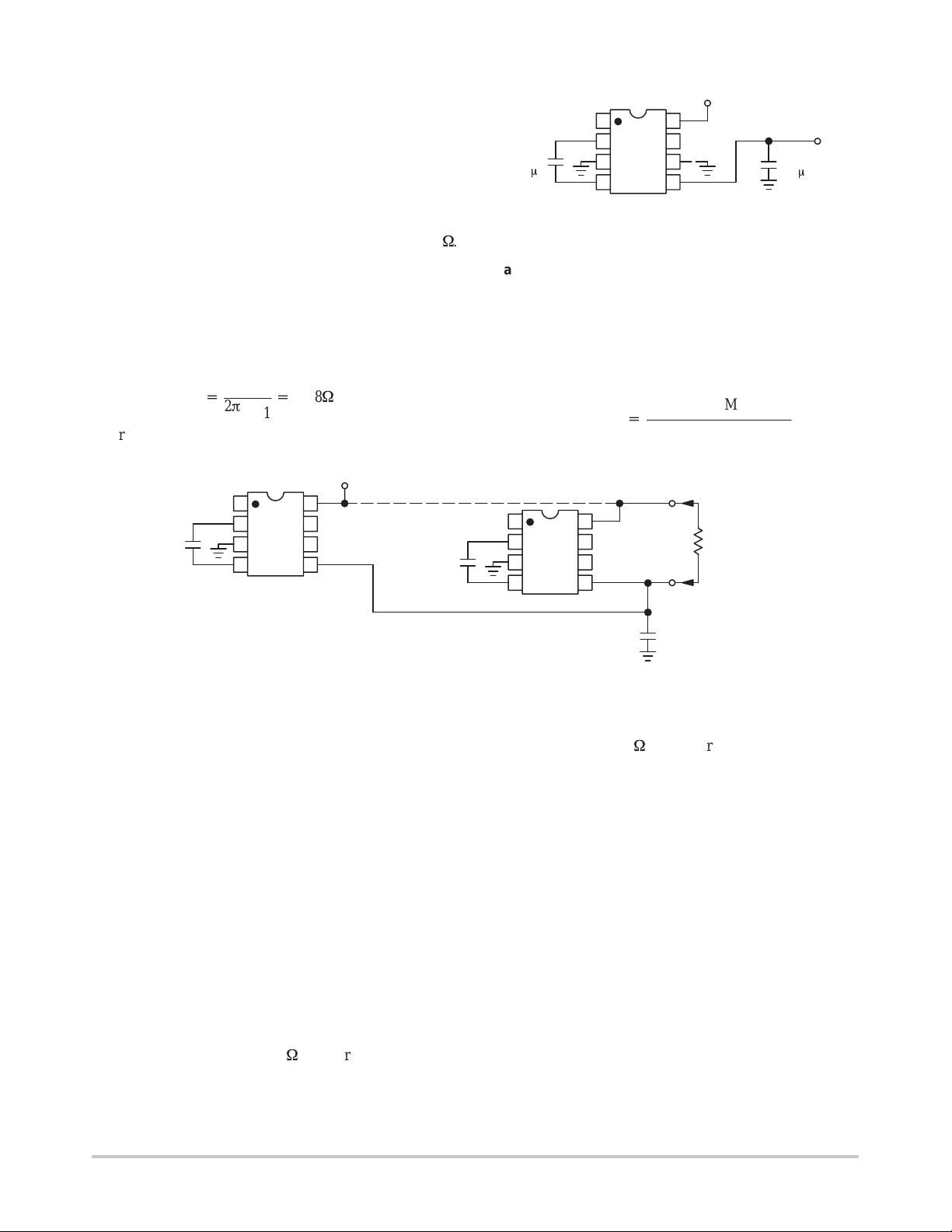
Parallel Devices
paralleled to reduce output resistance (Figure 4). The
reservoir capacitor, C
requires its own pump capacitor, C1. The resultant output
resistance would be approximately:
+
V
8
7
6
5
V
OUT
C2
10 mF
+
C1
10 mF
1
2
+
MC7660
3
4
Figure 3. Simple Negative Converter
Any number of MC7660 voltage converters may be
, serves all devices, while each device
2
R
(of MC7660)
R
OUT
OUT
+
n (number of devices)
8
7
6
5
C1
C1
1
2
MC7660
3
4
Figure 4. Paralleling Devices Lowers Output Impedance
Cascading Devices
The MC7660 may be cascaded as shown (Figure 5) to
produce larger negative multiplication of the initial supply
voltage. However, due to the finite efficiency of each device,
the practical limit is 10 devices for light loads. The output
voltage is defined by:
V
= –n (VIN)
OUT
where n is an integer representing the number of devices
cascaded. The resulting output resistance would be
approximately the weighted sum of the individual MC7660
R
values.
OUT
Changing the MC7660 Oscillator Frequency
It may be desirable in some applications (due to noise or
other considerations) to increase the oscillator frequency.
This is achieved by overdriving the oscillator from an
external clock, as shown in Figure 6. In order to prevent
possible device latch–up, a 1kW resistor must be used in
series with the clock output. In a situation where the designer
1
2
MC7660
3
4
8
7
6
5
R
L
C2
+
has generated the external clock frequency using TTL logic,
the addition of a 10kW pull–up resistor to V+ supply is
required. Note that the pump frequency with external
clocking, as with internal clocking, will be 1/2 of the clock
frequency. Output transitions occur on the positive–going
edge of the clock.
It is also possible to increase the conversion efficiency of
the MC7660 at low load levels by lowering the oscillator
frequency. This reduces the switching losses, and is
achieved by connecting an additional capacitor, C
OSC
, as
shown in Figure 7. Lowering the oscillator frequency will
cause an undesirable increase in the impedance of the pump
(C
) and the reservoir (C2) capacitors. To overcome this,
1
increase the values of C1 and C2 by the same factor that the
frequency has been reduced. For example, the addition of a
100pF capacitor between pin 7 (OSC) and pin 8 (V
+
) will
lower the oscillator frequency to 1kHz from its nominal
frequency of 10kHz (a multiple of 10), and necessitate a
corresponding increase in the values of C1 and C2 (from
10µF to 100µF).
http://onsemi.com
4
Page 5

MC7660
+
V
10 mF
*NOTE: V
1
2
+
MC7660
3
4
= –n V+ for 1.5 V ≤ V+ ≤ 10 V
OUT
“1”
8
7
6
5
Figure 5. Increased Output V oltage by Cascading Devices
10 mF
+
V
1
2
+
MC7660
3
4
8
1 k
7
6
5
+
V
W
CMOS
GATE
V
OUT
10 mF
+
Figure 6. External Clocking
+
V
8
7
6
5
C
OSC
V
OUT
C2
+
C1
1
2
+
MC7660
3
4
Figure 7. Lowering Oscillator Frequency
Positive V oltage Multiplication
The MC7660 may be employed to achieve positive
voltage multiplication using the circuit shown in Figure 8.
In this application, the pump inverter switches of the
MC7660 are used to charge C1 to a voltage level of V
+
– V
(where V+ is the supply voltage and VF is the forward voltage
drop of diode D1). On the transfer cycle, the voltage on C
plus the supply voltage (V+) is applied through diode D2 to
capacitor C2. The voltage thus created on C2 becomes (2 V+)
– (2 VF), or twice the supply voltage minus the combined
forward voltage drops of diodes D
The source impedance of the output (V
the output current, but for V
and D2.
1
) will depend on
+
= 5V and an output current of
OUT
10 mA, it will be approximately 60W.
10 mF
1
2
+
MC7660
3
4
1
2
3
4
“n”
MC7660
8
7
6
5
+
8
D1
7
6
5
V
+
10 mF
+
C1
V
D2
OUT
*
V
(2 V+) – (2 VF)
+
Figure 8. Positive V oltage Multiplier
Combined Negative V oltage Conversion and Positive
Supply Multiplication
Figure 9 combines the functions shown in Figures 3 and
8 to provide negative voltage conversion and positive
voltage multiplication simultaneously . This approach would
be, for example, suitable for generating +9V and –5V from
an existing +5V supply. In this instance, capacitors C
C3 perform the pump and reservoir functions, respectively,
for the generation of the negative voltage, while capacitors
C2 and C4 are pump and reservoir, respectively, for the
multiplied positive voltage. There is a penalty in this
configuration which combines both functions, however, in
that the source impedances of the generated supplies will be
somewhat higher due to the finite impedance of the common
charge pump driver at pin 2 of the device.
+
F
C1
1
2
MC7660
3
4
C2
1
+
V
8
D1
7
6
5
+
+
D2
+
V
–(V+ – VF)
V
(2 V+) – (2 VF)
OUT
C2
OUT
C3
OUT
C4
=
and
1
=
=
http://onsemi.com
5
Figure 9. Combined Negative Converter and
Positive Muliplier
Page 6

MC7660
Efficient Positive V oltage Multiplication/Conversion
Since the switches that allow the charge pumping
operation are bidirectional, the charge transfer can be
performed backwards as easily as forwards. Figure 10 shows
a MC7660 transforming –5V to +5V (or +5V to +10V , etc.).
The only problem here is that the internal clock and
1
2
C1
10 mF
+
MC7660
3
4
Figure 10. Positive V oltage Conversion
V oltage Splitting
The same bidirectional characteristics used in Figure 10
can also be used to split a higher supply in half, as shown in
Figure 11. The combined load will be evenly shared between
the two sides. Once again, a high value resistor to the L V pin
ensures start–up. Because the switches share the load in
V
8
7
6
5
switch–drive section will not operate until some positive
voltage has been generated. An initial inefficient pump, as
shown in Figure 9, could be used to start this circuit up, after
which it will bypass the other (D
and D2 in Figure 9 would
1
never turn on), or else the diode and resistor shown dotted
in Figure 10 can be used to ”force” the internal regulator on.
–
= –V
OUT
+
1 M
W
V– INPUT
10 mF
parallel, the output impedance is much lower than in the
standard circuits, and higher currents can be drawn from the
device. By using this circuit, and then the circuit of Figure
5, +15V can be converted (via +7.5V and –7.5V) to a
nominal –15V, though with rather high series resistance
(~250W).
R
V
R
L1
OUT
L2
+
50 mF
)
–
*
V
V
+
2
50 mF
+
–
100 k
50 mF
+
1
2
MC7660
3
100 k
W
W
+
–
4
8
7
1 M
W
6
5
V
–
V
Figure 11. Splitting a Supply in Half
http://onsemi.com
6
Page 7

MC7660
TYPICAL PERFORMANCE CHARACTERISTICS
12
10
8
6
4
2
SUPPLY VOLTAGE (VOLTS)
0
–55 –25 0 25 50 75 125
SUPPLY VOLTAGE RANGE
100
TEMPERATURE (°C)
Figure 12. Operating Voltage versus
Temperature
10 k
W
TA = +25°C
1 k
100
10
OUTPUT SOURCE RESISTANCE ( )
01234 6 8
SUPPLY VOLTAGE (VOLTS)
57
Figure 14. Output Source Resistance versus
Supply V oltage
100
98
I
= 1 mA
OUT
96
94
92
I
= 15 mA
OUT
90
88
86
EFFICIENCY (%)
84
POWER CONVERSION
TA = +25°C
V+ = +5 V
82
80
100 1 k 10 k
OSCILLATOR FREQUENCY (Hz)
Figure 13. Power Conversion Efficiency
versus Oscillator Frequency
350
W
I
300
250
200
150
100
50
0
OUTPUT SOURCE RESISTANCE ( )
–55 –25 0 25 50 75 125
= 1 mA
OUT
V+ = +2 V
V+ = +5 V
TEMPERATURE (°C)
Figure 15. Output Source Resistance
versus T emperature
100
10 k
TA = +25°C
V+ = +5 V
1 k
100
OSCILLATOR FREQUENCY (Hz)
10
1 10 100 1000 10 k
OSCILLATOR CAPACITANCE (pF)
Figure 16. Frequency of Oscillation versus
Oscillator Capacitance
OSCILLATOR FREQUENCY (kHz)
http://onsemi.com
7
20
V+ = +5 V
18
16
14
12
10
8
6
–55 –25 0 25 50 75 125
TEMPERATURE (°C)
100
Figure 17. Unloaded Oscillator Frequency
versus T emperature
Page 8

MC7660
TYPICAL CHARACTERISTICS (Cont.)
0
–1
–2
–3
–4
–5
–6
–7
–8
OUTPUT VOLTAGE (VOLTS)
–9
–10
0102030 506040
OUTPUT CURRENT (mA)
TA = +25°C
LV OPEN
Figure 18. Output Voltage versus
Output Current
100
90
80
70
60
50
40
30
20
10
POWER CONVERSION EFFICIENCY (%)
TA = +25°C
V+ = +2 V
0
0 1.5 3.0 4.5 6.0 9.0
LOAD CURRENT (mA)
Figure 20. Supply Current and Power
Conversion Efficiency versus Load Current
7.5
5
4
TA = +25°C
V+ = +5 V
3
2
1
0
–1
–2
–3
OUTPUT VOLTAGE (VOLTS)
–4
80 9070
100
–5
010 80
SLOPE 55
20 30 40 50 60 70
LOAD CURRENT (mA)
W
Figure 19. Output Voltage versus
Load Current
20
18
SUPPLY CURRENT (mA)
16
14
12
10
8
6
4
2
0
100
90
80
70
60
50
40
30
20
10
0
0 10203040 60
POWER CONVERSION EFFICIENCY (%)
LOAD CURRENT (mA)
TA = +25°C
V+ = +5 V
50
100
90
80
70
60
50
40
30
20
10
0
SUPPLY CURRENT (mA)
Figure 21. Supply Current and Power
Conversion Efficiency versus Load Current
2
TA = +25°C
1
V+ = +2 V
0
–1
OUTPUT VOLTAGE (VOLTS)
–2
012 345 8
LOAD CURRENT (mA)
SLOPE 150
W
67
Figure 22. Output Voltage versus Load Current
http://onsemi.com
8
Page 9

MC7660
P ACKAGE DIMENSIONS
8–Pin SOIC
PLASTIC PACKAGE
CASE 751–06
ISSUE T
A
E
B
C
A1
D
58
0.25MB
1
H
4
e
M
h
X 45
_
q
C
A
SEATING
PLANE
0.10
L
B
SS
A0.25MCB
NOTES:
1. DIMENSIONING AND TOLERANCING PER ASME
Y14.5M, 1994.
2. DIMENSIONS ARE IN MILLIMETER.
3. DIMENSION D AND E DO NOT INCLUDE MOLD
PROTRUSION.
4. MAXIMUM MOLD PROTRUSION 0.15 PER SIDE.
5. DIMENSION B DOES NOT INCLUDE DAMBAR
PROTRUSION. ALLOWABLE DAMBAR
PROTRUSION SHALL BE 0.127 TOTAL IN EXCESS
OF THE B DIMENSION AT MAXIMUM MATERIAL
CONDITION.
MILLIMETERS
DIM MIN MAX
A 1.35 1.75
A1 0.10 0.25
B 0.35 0.49
C 0.19 0.25
D 4.80 5.00
E
3.80 4.00
1.27 BSCe
H 5.80 6.20
h
0.25 0.50
L 0.40 1.25
0 7
q
__
http://onsemi.com
9
Page 10

Notes
MC7660
http://onsemi.com
10
Page 11

Notes
MC7660
http://onsemi.com
11
Page 12

MC7660
ON Semiconductor and are trademarks of Semiconductor Components Industries, LLC (SCILLC). SCILLC reserves the right to make changes
without further notice to any products herein. SCILLC makes no warranty , representation or guarantee regarding the suitability of its products for any particular
purpose, nor does SCILLC assume any liability arising out of the application or use of any product or circuit, and specifically disclaims any and all liability ,
including without limitation special, consequential or incidental damages. “Typical” parameters which may be provided in SCILLC data sheets and/or
specifications can and do vary in different applications and actual performance may vary over time. All operating parameters, including “Typicals” must be
validated for each customer application by customer’s technical experts. SCILLC does not convey any license under its patent rights nor the rights of others.
SCILLC products are not designed, intended, or authorized for use as components in systems intended for surgical implant into the body, or other applications
intended to support or sustain life, or for any other application in which the failure of the SCILLC product could create a situation where personal injury or
death may occur. Should Buyer purchase or use SCILLC products for any such unintended or unauthorized application, Buyer shall indemnify and hold
SCILLC and its officers, employees, subsidiaries, affiliates, and distributors harmless against all claims, costs, damages, and expenses, and reasonable
attorney fees arising out of, directly or indirectly , any claim of personal injury or death associated with such unintended or unauthorized use, even if such claim
alleges that SCILLC was negligent regarding the design or manufacture of the part. SCILLC is an Equal Opportunity/Affirmative Action Employer .
PUBLICATION ORDERING INFORMATION
NORTH AMERICA Literature Fulfillment:
Literature Distribution Center for ON Semiconductor
P.O. Box 5163, Denver, Colorado 80217 USA
Phone: 303–675–2175 or 800–344–3860 Toll Free USA/Canada
Fax: 303–675–2176 or 800–344–3867 Toll Free USA/Canada
Email: ONlit@hibbertco.com
Fax Response Line: 303–675–2167 or 800–344–3810 T oll Free USA/Canada
N. American Technical Support: 800–282–9855 Toll Free USA/Canada
EUROPE: LDC for ON Semiconductor – European Support
German Phone: (+1) 303–308–7140 (M–F 1:00pm to 5:00pm Munich Time)
Email: ONlit–german@hibbertco.com
French Phone: (+1) 303–308–7141 (M–F 1:00pm to 5:00pm Toulouse Time)
Email: ONlit–french@hibbertco.com
English Phone: (+1) 303–308–7142 (M–F 12:00pm to 5:00pm UK Time)
Email: ONlit@hibbertco.com
EUROPEAN TOLL–FREE ACCESS*: 00–800–4422–3781
*Available from Germany, France, Italy, England, Ireland
CENTRAL/SOUTH AMERICA:
Spanish Phone: 303–308–7143 (Mon–Fri 8:00am to 5:00pm MST)
Email: ONlit–spanish@hibbertco.com
ASIA/PACIFIC : LDC for ON Semiconductor – Asia Support
Phone: 303–675–2121 (Tue–Fri 9:00am to 1:00pm, Hong Kong Time)
T oll Free from Hong Kong & Singapore:
001–800–4422–3781
Email: ONlit–asia@hibbertco.com
JAPAN: ON Semiconductor, Japan Customer Focus Center
4–32–1 Nishi–Gotanda, Shinagawa–ku, T okyo, Japan 141–8549
Phone: 81–3–5740–2745
Email: r14525@onsemi.com
ON Semiconductor Website: http://onsemi.com
For additional information, please contact your local
Sales Representative.
http://onsemi.com
12
MC7660/D
 Loading...