

Page 1
Order this document by MC75172B/D
!
The Motorola MC75172B/174B Quad Line drivers are differential high
speed drivers designed to comply with the EIA–485 Standard. Features
include three–state outputs, thermal shutdown, and output current limiting in
both directions. These devices also comply with EIA–422–A, and CCITT
Recommendations V.11 and X.27.
The MC75172B/174B are optimized for balanced multipoint bus
transmission at rates in excess of 10 MBPS. The outputs feature wide
common mode voltage range, making them suitable for party line
applications in noisy environments. The current limit and thermal shutdown
features protect the devices from line fault conditions. These devices offer
optimum performance when used with the MC75173 and MC75175 line
receivers.
Both devices are available in 16–pin plastic DIP and 20–pin wide body
surface mount packages.
• Meets EIA–485 Standard for Party Line Operation
• Meets EIA–422–A and CCITT Recommendations V.11 and X.27
• Operating Ambient Temperature: –40°C to +85°C
• High Impedance Outputs
• Common Mode Output Voltage Range: –7 to 12 V
• Positive and Negative Current Limiting
• Transmission Rates in Excess of 10 MBPS
• Thermal Shutdown at 150°C Junction Temperature, (±
• Single 5.0 V Supply
• Pin Compatible with TI SN75172/4 and NS µA96172/4
• Interchangeable with MC3487 and AM26LS31 for EIA–422–A
Applications
ā
20°C)
QUAD EIA–485 LINE DRIVERS
SEMICONDUCTOR
TECHNICAL DATA
P SUFFIX
PLASTIC PACKAGE
CASE 648
DW SUFFIX
PLASTIC PACKAGE
CASE 751D
(SO–20L)
ORDERING INFORMATION
Operating
Device
MC75172BDW
MC75174BDW SO–20L
MC75174BP Plastic DIP
Temperature Range
TA = –40° to +85°C
Package
SO–20L
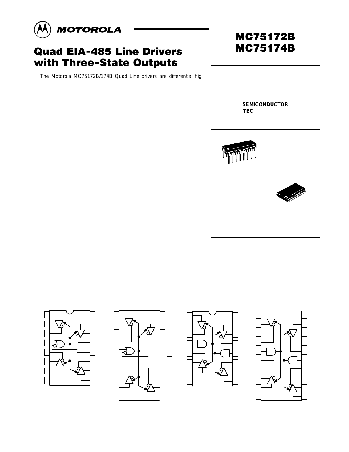
MC75172B MC75174B
1A
1Y
1Z
En
2Z
2Y
2A
Gnd
1
2
3
4
5
6
7
8
P Package
16
15
14
13
12
11
10
V
4A
4Y
4Z
En
3Z
3Y
9
3A
MOTOROLA ANALOG IC DEVICE DATA
1
1A
CC
2
1Y
3
NC
4
1Z NC
5
En
6
2Z
7
NC
8
2Y
9
2A
10 11
Gnd
DW Package
PIN CONNECTIONS
20
19
18
17
16
15
14
13
12
V
4A
4Y
4Z
En
3Z
NC
3Y
3A
CC
1A
1Y
1Z
En
12
2Z
2Y
2A
Gnd
1
2
3
4
5
6
7
8
1
1A
16
V
CC
2
1Y
15
4A
3
NC
14
4Y
4
1Z
13
4Z
En
5
En
12
12
34
2Z
11
10
9
P Package
Motorola, Inc. 1996 Rev 1
6
3Z
7
NC
3Y
2Y
8
3A
9
2A
10 11
Gnd
DW Package
20
19
18
17
16
15
14
13
12
V
4A
4Y
NC
4Z
En
34
3Z
NC
3Y
3A
CC
1
Page 2
MC75172B MC75174B
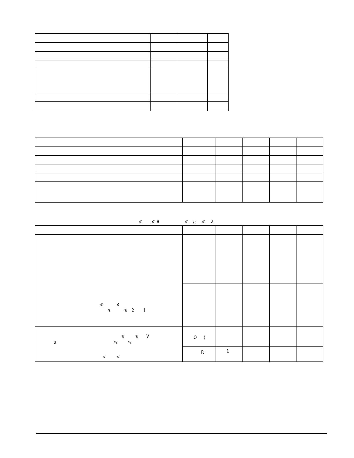
MAXIMUM RATINGS
Rating Symbol Value Unit
Power Supply Voltage V
Input Voltage (Data, Enable) V
Input Current (Data, Enable) I
Applied Output Voltage, when in 3–State Condition
(VCC = 5.0 V)
Applied Output Voltage, when VCC = 0 V V
Output Current I
Storage Temperature T
Devices should not be operated at these limits. The “Recommended Operating Conditions” table provides
for actual device operation.
CC
in
in
V
za
zb
O
stg
RECOMMENDED OPERATING CONDITIONS
Characteristic Symbol Min Typ Max Unit
Power Supply Voltage V
Input Voltage (All Inputs) V
Output Voltage in 3–State Condition, or when VCC = 0 V V
Output Current (Normal data transmission) I
Operating Ambient Temperature (see text)
EIA–485
EIA–422
All limits are not necessarily functional concurrently.
–0.5, +7.0 Vdc
+7.0 Vdc
–24 mA
–10, +14 Vdc
±14
Self–Limiting –
–65, +150 °C
CC
in
cm
O
T
A
+4.75 +5.0 +5.25 Vdc
0 – V
–7.0 – +12 Vdc
–65 – +65 mA
–40
0
–
–
CC
+85
+85
Vdc
°C
ELECTRICAL CHARACTERISTICS (–40°C
Characteristic Symbol Min Typ Max Unit
Output Voltage
Single–Ended Voltage
IO = 0
High @ IO = –33 mA
Low @ IO = +33 mA
Differential Voltage
Open Circuit (IO = 0)
RL = 54 Ω (Figure 1)
Change in Differential*, RL = 54 Ω (Figure 1)
Differential Voltage, RL = 100 Ω (Figure 1)
Change in Differential*, RL = 100 Ω (Figure 1)
Differential V oltage, –7.0 V p Vcm p 12 V (Figure 2)
Change in Differential*, –7.0 V p Vcm p12 V (Figure 2)
Offset Voltage, RL = 54 Ω (Figure 1)
Change in Offset*, RL = 54 Ω (Figure 1)
Output Current (Each Output)
Power Off Leakage, VCC = 0, –7.0 V p VO p 12 V
Leakage in 3–State Mode, –7.0 V p VO p 12 V
Short Circuit Current to Ground
Short Circuit Current, –7.0 V p VO p 12 V
*Vin switched from 0.8 to 2.0 V.
Typical values determined at 25°C ambient and 5.0 V supply.
p
TA p 85°C, 4.75 V p VCC p 5.25 V, unless otherwise noted.)
V
V
V
V
OD1
V
OD2
∆V
V
OD2A
∆V
OD2A
V
OD3
∆V
V
∆VOS
I
O(off)
I
OZ
I
OSR
I
OS
O
OH
OL
OD2
OD3
OS
0
–
–
1.5
1.5
–
–
–
1.5
–
–
–
–50
–50
–150
–250
–
4.0
1.6
3.4
2.3
5.0
2.2
5.0
–
5.0
2.9
5.0
0
0
–
–
6.0
–
–
6.0
5.0
200
–
200
5.0
200
–
200
+50
+50
+150
+250
Vdc
mVdc
Vdc
mVdc
Vdc
mVdc
Vdc
mVdc
µA
mA
2
MOTOROLA ANALOG IC DEVICE DATA
Page 3
MC75172B MC75174B
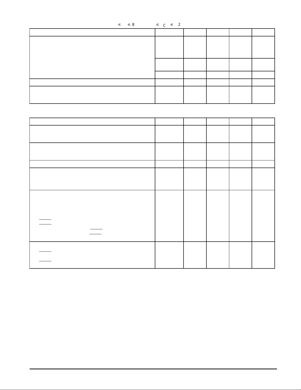
ELECTRICAL CHARACTERISTICS (–40°C
Characteristics
Inputs
Low Level Voltage (Pins 4 & 12, MC75174B only)
Low Level Voltage (All Other Pins)
High Level Voltage (All Inputs)
Current @ Vin = 2.7 V (All Inputs)
Current @ Vin = 0.5 V (All Inputs)
Clamp Voltage (All Inputs, Iin = –18 mA) V
Thermal Shutdown Junction Temperature T
Power Supply Current (Outputs Open, VCC = 5.25 V)
Outputs Enable
Outputs Disabled
TIMING CHARACTERISTICS (T
Characteristics
Propagation Delay – Input to Single–ended Output (Figure 3)
Output Low–to–High
Output High–to–Low
Propagation Delay – Input to Differential Output (Figure 4)
Input Low–to–High
Input High–to–Low
Differential Output Transition T ime (Figure 4) tdr, t
Skew Timing
t
– t
PLHD
Max – Min t
Max – Min t
Enable Timing
Single–ended Outputs (Figure 5)
Enable to Active High Output
Enable to Active Low Output
Active High to Disable (using Enable)
Active Low to Disable (using Enable)
Enable
to Active High Output (MC75172B only)
Enable
to Active Low Output (MC75172B only)
Active High to Disable (using Enable
Active Low to Disable (using Enable
Differential Outputs (Figure 6)
Enable to Active Output
Enable
to Active Output (MC75172B only)
Enable to 3–State Output
Enable
to 3–State Output (MC75172B only)
for Each Driver
PHLD
Within a Package
PLHD
Within a Package
PHLD
= 25°C, VCC = 5.0 V)
A
, MC75172B only)
, MC75172B only)
p
TAp
85°C, 4.75 V p VCC p 5.25 V, unless otherwise noted.)
Symbol Min Typ Max Unit
V
V
Symbol Min Typ Max Unit
t
PLH(D)
t
PHL(D)
t
PZH(E)
t
PZL(E)
t
PHZ(E)
t
PLZ(E)
t
PZH(E)
t
PZL(E)
t
PHZ(E)
t
PLZ(E)
t
PZD(E)
t
PZD(E)
t
PDZ(E)
t
PDZ(E)
IL(A)
IL(B)
V
I
IH
I
I
CC
t
PLH
t
PHL
t
SK1
t
SK2
t
SK3
0
0
IH
IL
IK
jts
df
2.0
–
–100
–1.5 – – Vdc
– +150 – °C
–
–
–
–
–
–
– 19 25 ns
–
–
–
–
–
–
–
–
–
–
–
–
–
–
–
–
–
–
0.2
–15
60
30
23
18
15
17
0.2
1.5
1.5
48
20
35
30
58
28
38
36
47
56
32
40
0.7
0.8
V
CC
20
–
70
40
30
30
25
25
–
–
–
60
30
45
50
70
35
50
50
–
–
–
–
Vdc
µA
mA
ns
ns
ns
ns
ns
MOTOROLA ANALOG IC DEVICE DATA
3
Page 4
V
(0.8 or 2.0 V)
in
V
in
S.G.
MC75172B MC75174B
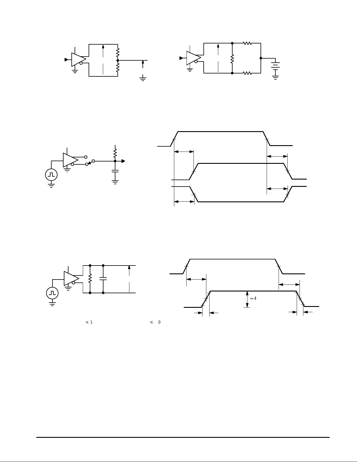
Figure 1. VDD Measurement Figure 2. Common Mode T est
V
V
in
1.5 V
t
PLH
t
PHL
CC
3.0 V
3.0 V
V
OD3
375
58
375
3.0 V
V
CC
RL/2
V
OD2,A
RL/2
V
OS
(0.8 or 2.0 V)
Figure 3. Propagation Delay , Single–Ended Outputs
V
V
CC
Y
2.3 V
27
Ω
Output
Z
15 pF
in
Output Y
Output Z
+
VCM = 12 to –7.0 V
1.5 V
t
PHL
3.0 V
t
PLH
3.0 V
0 V
V
OL
V
OH
Figure 4. Propagation Delay , Differential Outputs
V
CC
V
in
54
S.G.
NOTES: 1. S.G. set to: f p 1.0 MHz; duty cycle = 50%; tr, tf, p5.0 ns.
2.t
= t
SK1
3.t
computed by subtracting the shortest t
SK2
4.t
computed by subtracting the shortest t
SK3
PLHD
– t
PHLD
for each driver.
50 pF
V
OD
from the longest t
PLHD
from the longest t
PHLD
3.0 V
1.5 V
V
in
t
PLHD
1.5 V
V
OD
50%
[
4.6 V
–1.5 V
t
dr
of the 4 drivers within a package.
PLHD
of the 4 drivers within a package.
PHLD
1.5 V
t
PHLD
t
df
0 V
1.5 V
50%
–1.5 V
4
MOTOROLA ANALOG IC DEVICE DATA
Page 5

MC75172B MC75174B
Figure 5. Enable Timing, Single–Ended Outputs
0 or 3.0 V
V
in
3.0 V
0 or 3.0 V
V
3.0 V
in
S.G.
S.G.
V
CC
V
V
out
out
1.5 V
t
PZH(E)
1.5 V
t
PZL(E)
2.3 V
2.3 V
V
in
V
out
110
50 pF
V
CC
110
Ω
50 pF
Ω
V
CC
V
in
V
out
3.0 V
1.5 V
3.0 V
1.5 V
t
PHZ(E)
t
PLZ(E)
0 V
0 V
0.5 V
0.5 V
V
OH
V
OL
Figure 6. Enable Timing, Differential Outputs
V
CC
0 or 3.0 V
V
in
3.0 V
S.G.
NOTES: 1. S.G. set to: f p 1.0 MHz; duty cycle = 50%; tf, tf, p 5.0 ns.
2.Vin is inverted for Enable
54
measurements.
50 pF
V
V
OD
3.0 V
1.5 V
in
t
PZD(E)
V
OD
0
Disabled
1.5 V
Active
1.5 V
t
PDZ(E)
0 V
1.5 V
0
Disabled
MOTOROLA ANALOG IC DEVICE DATA
5
Page 6

MC75172B MC75174B
Figure 7. Single–Ended Output V oltage
versus Output Sink Current
2.0
1.5
1.0
, OUTPUT VOL TAGE (V)
OL
0.5
V
4.75V pVCCp
°
C
TA = 25
0
02010 30 40 50 60 70
IOL, OUTPUT CURRENT (mA)
Figure 9. Single–Ended Output V oltage
versus Output Source Current
5.0
4.0
3.0
VCC = 5.25 V
VCC = 5.00 V
VCC = 4.75 V
5.25 V
2.0
1.75
1.5
, OUTPUT VOL TAGE (V)
OL
1.25
V
1.0
–40 0–20
4.0
3.75
Figure 8. Single–Ended Output V oltage
versus T emperature
IOL = 27.8 mA
IOL = 20.0 mA
4.75 V p VCC p 5.25 V
TA, AMBIENT TEMPERATURE (
°
C)
Figure 10. Single–Ended Output
V oltage versus Temperature
IOH = –20.0 mA
IOH = –27.8 mA
85604020
, OUTPUT VOL TAGE (V)
2.0
OH
V
1.0
4.0
3.0
2.0
1.0
, DIFFERENTIAL OUTPUT VOLTAGE (V)
OD
V
0
–100–30–20 –40 –5060–60
IOH, OUTPUT CURRENT (mA)
Figure 11. Output Differential Voltage
versus Load Current
VCC = 5.25 V
VCC = 5.0 V
VCC = 4.75 V
0.8 or
2.0 V
10
I
V
O
OD
5030 40020
IO, OUTPUT CURRENT (mA)
TA = 25°C
TA = 25°C
–70
70
3.5
, OUTPUT VOL TAGE (V)
OH
V
3.25
–40 0–20 6040
TA, AMBIENT TEMPERATURE (
20
Figure 12. Output Differential Voltage
versus T emperature
4.0
3.0
IO = 20.0 mA
2.0
1.0
, DIFFERENTIAL OUTPUT VOLTAGE (V)
OD
V
0
–40
0.8 or
2.0 V
I
V
O
OD
0
TA, AMBIENT TEMPERATURE (
VCC = 4.75 V
85
°
C)
IO = 27.8 mA
VCC = 4.75 V
20 40 60–20
°
C)
85
6
MOTOROLA ANALOG IC DEVICE DATA
Page 7

MC75172B MC75174B
A)
µ
, LEAKAGE CURRENT (
I
2.0
1.0
–1.0
OZ
–2.0
5.0
0
–7.0
Figure 13. Output Leakage Current
versus Output Voltage
TA = 25°C
En = Low, En
1.0–3.0 5.0 9.0 12 –40
Vz, APPLIED OUTPUT VOLTAGE (V)
= High
Figure 15. Input Current
versus Input V oltage
A)I ,
µ
–5.0
, LEAKAGE CURRENT (
–10
OZ
I
OX
–15
–20
150
20
15
10
5.0
Figure 14. Output Leakage Current
versus T emperature
V
= +12 V
0
out
V
= 7.0 V
out
En = Low, En = High
or VCC = 0 V
0–20
TA, AMBIENT TEMPERATURE (
20
40
60
°
C)
85
Figure 16. Short Circuit Current
versus Common Mode V oltage
0
A)
µ
–5.0
–10
–15
, INPUT CURRENT (
in
I
–20
–25
–0.5 3.52.51.5
Enable
Pins
Driver
Inputs
4.75 p VCC p 5.25 V
TA = 25
Vin, INPUT VOLTAGE (V)
90
30
0
–30
°
C
4.5
, SHORT CIRCUIT CURRENT (mA)
–90
OS
I
–150
–7.0 –3.05.5 5.0 121.0
Normally Low Output
Vz, APPLIED OUTPUT VOLTAGE (V)
Normally High Output
TA = 25°C
p
VCC p 5.25 V
4.75
9.00.5
MOTOROLA ANALOG IC DEVICE DATA
7
Page 8

MC75172B MC75174B
HLHHXXHLL
LHHXXLLHH
HLXXLLHLL
LXXLLHLZH
APPLICATIONS INFORMATION
Description
The MC75172B and MC75174B are differential line drivers
designed to comply with EIA–485 Standard (April 1983) for
use in balanced digital multipoint systems containing multiple
drivers. The drivers also comply with EIA–422–A and CCITT
Recommendations V.11 and X.27. The drivers meet the
EIA–485 requirement for protection from damage in the event
that two or more drivers attempt to transmit data
simultaneoulsy on the same cable. Data rates in excess of 10
MBPS are possible, depending on the cable length and cable
characteristics. A single power supply, 5.0 V, ±5%, is required
at a nominal current of 60 mA, plus load currents.
Outputs
Each output (when active) will be a low or a high voltage,
which depends on the input state and the load current (see
Table 1, 2 and Figures 7 to 10). The graphs apply to each
driver, regardless of how many other drivers within the
package are supplying load current.
T able 1. MC75172B Truth Table
Enables Outputs
Data Input
H H X H L
T able 2. MC75174B Truth Table
Data Input Enable
H H H L
L
X L Z Z
H = Logic high, L = Logic low, X = Irrelevant, Z = High impedance
The two outputs of a driver are always complementary. A
“high” output can only source current out, while a “low” output
can only sink current (except for short circuit current – see
Figure 16).
The outputs will be in the high impedance mode when:
the Enable inputs are set according to Table 1 or 2; a)
b)
VCC is less than 1.5 V;
c)
the junction temperature exceeds the trip point of the
thermal shutdown circuit (see below). When in this
condition, the output’s source and sink capability are
shut off, and only leakage currents will flow (see
Figures 13, 14). Disabled outputs may be taken to any
voltage between –7.0 V and 12 V without damage.
EN EN Y Z
Outputs
Y Z
H
L
H
L
H
Z
H
The drivers are protected from short circuits by two
methods:
a)
Current limiting is provided at each output, in both the
source and sink direction, for shorts to any voltage
within the range of 12V to –7.0V , with respect to circuit
ground (see Figure 16). The short circuit current will flow
until the fault is removed, or until the thermal shutdown
circuit activates (see below). The current limiting circuit
has a negative temperature coefficient and requires no
resetting upon removal of the fault condition.
b)
A thermal shutdown circuit disables the outputs when
the junction temperature reaches 150°C, ±ā20°C. The
thermal shutdown circuit has a hysteresis of ≈ 12°C to
prevent oscillations. When this circuit activates, the
output stage of each driver is put into the high
impedance mode, thereby shutting off the output
currents. The remainder of the internal circuitry remains
biased. The outputs will become active once again as
the IC cools down.
Driver Inputs
The driver inputs determine the state of the outputs in
accordance with Tables 1 and 2. The driver inputs have a
nominal threshold of 1.2 V, and their voltage must be kept
within the range of 0 V to VCC for proper operation. If the
voltage is taken more than 0.5 V below ground, excessive
currents will flow, and proper operation of the drivers will be
affected. An open pin is equivalent to a logic high, but good
design practices dictate that inputs should never be left open.
The characteristics of the driver inputs are shown in Figure
15. This graph is not affected by the state of the Enable pins.
Enable Logic
Each driver’s outputs are active when the Enable inputs
(Pins 4 and 12) are true according to Tables 1 and 2.
The Enable inputs have a nominal threshold of 1.2 V and
their voltage must be kept within the range of 0 V to VCC for
proper operation. If the voltage is taken more than 0.5 V
below ground, excessive currents will flow, and proper
operation of the drivers will be affected. An open pin is
equivalent to a logic high, but good design practices dictate
that inputs should never be left open. The Enable input
characteristics are shown in Figure 15.
Operating Temperature Range
The minimum ambient operating temperature is listed as
–40°C to meet EIA–485 specifications, and 0°C to meet
EIA–422–A specifications. The higher VOD required by
EIA–422–A is the reason for the narrower temperature range.
8
MOTOROLA ANALOG IC DEVICE DATA
Page 9

MC75172B MC75174B
The maximum ambient operating temperature (applicable
to both EIA–485 and EIA–422–A) is listed as 85°C. However,
a lower ambient may be required depending on system use
(i.e. specifically how many drivers within a package are used)
and at what current levels they are operating. The maximum
power which may be dissipated within the package is
determined by:
T
Jmax–TA
+
R
q
JA
= package thermal resistance (typical
θJA
where:
PD
max
R
70°C/W for the DIP package, 85°C/W for SOIC
package);
T
= max. operating junction
Jmax
temperature, and
TA = ambient temperature.
Since the thermal shutdown feature has a trip point of
150°C, ± 20°C, T
is selected to be 130°C. The power
Jmax
dissipated within the package is calculated from:
PD
= {[(VCC – VOH) • IOH] + VOL • IOL)} each driver
= + (VCC • ICC)
where:
VCC = the supply voltage;
VOH, VOL are measured or estimated from
Figures 7 to 10;
ICC = the quiescent power supply current
(typical 60 mA).
As indicated in the equation, the first term (in brackets)
must be calculated and summed for each of the four drivers,
while the last term is common to the entire package.
Example 1:
TA = 25°C, IOL = IOH = 55 mA for each driver,
VCC = 5.0 V, DIP package. How many drivers per package
can be used?
Maximum allowable power dissipation is:
PD
max
130°C*25°C
+
70°CńW
+
1.5 W
Since the power supply current of 60 mA dissipates
300 mW, that leaves 1.2 W (1.5 W – 0.3 W) for the drivers.
From Figures 7 and 9, VOL [1.75 V , and VOH [3.85 V . The
power dissipated in each driver is:
{(5.0 – 3.85) • 0.055} + (1.75 • 0.055) = 160 mW.
Since each driver dissipates 160 mW, the four drivers per
package could be used in this application
Example 2:
TA = 85°C, IOL = 27.8 mA, IOH = 20 mA for each
driver, VCC = 5.0 V, SOIC package. How many drivers per
package can be used?
Maximum allowable power dissipation is:
130
°C
*
PD
max
+
85
°C
85°C
ń
W
+
0.53 W
Since the power supply current of 60 mA dissipates
300 mW, that leaves 230 mW (530 mW – 300 mW) for the
drivers. From Figures 8 and 10 (adjusted for VCC = 5.0 V),
VOL [1.38 V, and VOH [4.27 V. The power dissipated in
each driver is:
{(5.0 – 4.27) • 0.020} + (1.38 • 0.0278) = 53 mW
Since each driver dissipates 53 mW, the use of all four
drivers in a package would be marginal. Options include
reducing the load current, reducing the ambient temperature,
and/or providing a heat sink.
System Requirements
EIA–485 requires each driver to be capable of transmitting
data differentially to at least 32 unit loads, plus an equivalent
DC termination resistance of 60Ω, over a common mode
voltage of –7.0 to 12 V. A unit load (U.L.), as defined by
EIA–485, is shown in Figure 17.
Figure 17. Unit Load Definition
I
1.0 mA
–7.0 V
Reprinted from EIA–485, Electronic Industries Association,
Washington,DC.
–3.0 V
–0.8 mA
5.0 V
V
12 V
A load current within the shaded regions represents an
impedance of less than one U.L., while a load current of a
magnitude outside the shaded area is greater than one U.L.
A system’s total load is the sum of the unit load equivalents
of each receiver’s input current, and each disabled driver’s
output leakage current. The 60Ω termination resistance
mentioned above allows for two 120Ω terminating resistors.
Using the EIA–485 requirements (worst case limits), and
the graphs of Figures 7 and 9, it can be determined that the
maximum current an MC75172B or MC75174B driver will
source or sink is [65 mA.
System Example
An example of a typical EIA–485 system is shown in
Figure 18. In this example, it is assumed each receiver’s input
characteristics correspond to 1.0 U.L. as defined in Figure 17.
Each “off” driver, with a maximum leakage of ±50 µA over the
common mode range, presents a load of [0.06 U.L. The
total load for the active driver is therefore 8.3 unit loads, plus
the parallel combination of the two terminating resistors
(60Ω). It is up to the system software to control the driver
Enable pins to ensure that only one driver is active at any
time.
T ermination Resistors
Transmission line theory states that, in order to preserve
the shape and integrity of a waveform traveling along a cable,
the cable must be terminated in an impedance equal to its
characteristic impedance. In a system such as that depicted
in Figure 18, in which data can travel in both directions, both
physical ends of the cable must be terminated. Stubs, leading
to each receiver and driver, should be as short as possible.
Leaving off the terminations will generally result in
reflections which can have amplitudes of several volts above
VCC or below ground. These overshoots and undershoots
can disrupt the driver and/or receiver operation, create false
data, and in some cases damage components on the bus.
MOTOROLA ANALOG IC DEVICE DATA
9
Page 10

MC75172B MC75174B
Figure 18. T ypical EIA–485 System
TTL
En
TTL
D
#1
5 “off” drivers (@ 0.06 U.L. each),
+8 receivers (@ 1.0 U.L. each) = 8.3 Unit Loads
RT = 120 Ω at each end of the cable.
En
D
#6
R
T
R
T
TTL
R
TTL
#2
En
D
#2
TTLEnTTL
TTL
TTL
TTL
#3
#4
D
#3
120
Ω
Twisted
Pair
R
En
D
#4
R
R
TTL
#1
R
#6
TTL
#8
R
NOTES: 1. Terminating resistors RT must be located at the physical ends of the cable.
2.Stubs should be as short as possible.
3.Circuit ground of all drivers and receivers must be connected via a dedicated wire within the cable.
Do not rely on chassis ground or power line ground.
R
#7
TTL TTL
R
#5
TTL
En
D
#5
10
MOTOROLA ANALOG IC DEVICE DATA
Page 11

MC75172B MC75174B
Comparing System Requirements
Characteristic Symbol EIA–485 EIA–422–A V.11 and X.27
GENERATOR (DRIVER)
Output Impedance (Note 1) Z
Open Circuit Voltage
Differential
Single–Ended
Loaded Differential Voltage V
Differential Voltage Balance ∆V
Output Common Mode Range V
Offset Voltage V
Offset Voltage Balance ∆V
Short Circuit Current I
Leakage Current (VCC = 0) I
Output Rise/Fall Time (Note 2) tr, t
RECEIVER
Input Sensitivity V
Input Bias Voltage V
Input Common Mode Range V
Dynamic Input Impedance R
NOTES: 1. Compliance with V .11 and X.27 (Blue book) output impedance requires external resistors in series with the outputs of the MC75172B and MC75174B.
2.TB = Bit time.
V
V
out
OCD
OCS
OD
OD
CM
OS
OS
OS
OLK
th
bias
cm
in
Not Specified
1.5 to 6.0 V
t
6.0 V
1.5 to 5.0 V, w/54 Ω load
t
200 mV
–7.0 to +12 V Not Specified Not Specified
–1.0 t VOS t 3.0 V
t
200 mV
p
250 mA for –7.0 to
12 V
Not Specified
p
f
0.3 TB, w/54 Ω/1150 pF
load
± 200 mV ± 200 mV ± 300 mV
p
3.0 V
–7.0 to 12 V –7.0 to 7.0 V –7.0 to 7.0 V
Spec number of U.L.
t
100 Ω 50 10 100 Ω
p
6.0 V
p
6.0 V
q
2.0 V or q 0.5
V
, w/100 Ω load
OCD
p
400 mV
p
3.0 V
p
400 mV
p
150 mA to ground
p
100 µA to –0.25 V
thru 6.0 V
p
0.1 TB or p 20 ns,
w/100 Ω load
p
3.0 V
q
4 kΩ
p
6.0 V, w/3.9 kΩ, Load
p
6.0 V, w/3.9 kΩ, Load
q
2.0 V orq0.5 V
w/100 Ω load
t
400 mV
p
3.0 V
t
400 mV
p
150 mA to ground
p
100 µA to ± 0.25 V
p
0.1 TB or p 20
w/100 Ω load
p
3.0 V
q
4 kΩ
OCD
ns,
,
Additional Information
Copies of the EIA Recommendations (EIA–485 and EIA–422–A) can be obtained from the Electronics Industries Association,
Washington, D.C. (202–457–4966). Copies of the CCITT Recommendations (V.11 and X.27) can be obtained from the United
States Department of Commerce, Springfield, V A (703–487–4600).
MOTOROLA ANALOG IC DEVICE DATA
11
Page 12

MC75172B MC75174B
–A–
916
B
18
F
H
G
D
16 PL
0.25 (0.010) T
–A–
20
1
11
10
D20X
M
0.010 (0.25) B
18X
G
A
T
S
–B–
S
K
C
SEATING
–T–
PLANE
K
M
M
A
P10X
0.010 (0.25)
S
C
SEATING
–T–
PLANE
OUTLINE DIMENSIONS
P SUFFIX
PLASTIC PACKAGE
CASE 648–08
ISSUE R
L
J
DW SUFFIX
PLASTIC PACKAGE
CASE 751D–04
(SO–20L)
ISSUE E
M
M
B
J
F
M
M
R
X 45
NOTES:
1. DIMENSIONING AND TOLERANCING PER ANSI
Y14.5M, 1982.
2. CONTROLLING DIMENSION: INCH.
3. DIMENSION L TO CENTER OF LEADS WHEN
FORMED PARALLEL.
4. DIMENSION B DOES NOT INCLUDE MOLD FLASH.
5. ROUNDED CORNERS OPTIONAL.
DIM MIN MAX MIN MAX
A 0.740 0.770 18.80 19.55
B 0.250 0.270 6.35 6.85
C 0.145 0.175 3.69 4.44
D 0.015 0.021 0.39 0.53
F 0.040 0.70 1.02 1.77
G 0.100 BSC 2.54 BSC
H 0.050 BSC 1.27 BSC
J 0.008 0.015 0.21 0.38
K 0.110 0.130 2.80 3.30
L 0.295 0.305 7.50 7.74
M 0 10 0 10
S 0.020 0.040 0.51 1.01
NOTES:
1. DIMENSIONING AND TOLERANCING PER
ANSI Y14.5M, 1982.
2. CONTROLLING DIMENSION: MILLIMETER.
3. DIMENSIONS A AND B DO NOT INCLUDE
MOLD PROTRUSION.
4. MAXIMUM MOLD PROTRUSION 0.150
(0.006) PER SIDE.
5. DIMENSION D DOES NOT INCLUDE
DAMBAR PROTRUSION. ALLOWABLE
DAMBAR PROTRUSION SHALL BE 0.13
(0.005) TOTAL IN EXCESS OF D
DIMENSION AT MAXIMUM MATERIAL
CONDITION.
DIM MIN MAX MIN MAX
A 12.65 12.95 0.499 0.510
B 7.40 7.60 0.292 0.299
C 2.35 2.65 0.093 0.104
D 0.35 0.49 0.014 0.019
_
F 0.50 0.90 0.020 0.035
G 1.27 BSC 0.050 BSC
J 0.25 0.32 0.010 0.012
K 0.10 0.25 0.004 0.009
M 0 7 0 7
__
P 10.05 10.55 0.395 0.415
R 0.25 0.75 0.010 0.029
MILLIMETERSINCHES
____
INCHESMILLIMETERS
__
Motorola reserves the right to make changes without further notice to any products herein. Motorola makes no warranty , representation or guarantee regarding
the suitability of its products for any particular purpose, nor does Motorola assume any liability arising out of the application or use of any product or circuit, and
specifically disclaims any and all liability, including without limitation consequential or incidental damages. “T ypical” parameters which may be provided in Motorola
data sheets and/or specifications can and do vary in different applications and actual performance may vary over time. All operating parameters, including “Typicals”
must be validated for each customer application by customer’s technical experts. Motorola does not convey any license under its patent rights nor the rights of
others. Motorola products are not designed, intended, or authorized for use as components in systems intended for surgical implant into the body, or other
applications intended to support or sustain life, or for any other application in which the failure of the Motorola product could create a situation where personal injury
or death may occur. Should Buyer purchase or use Motorola products for any such unintended or unauthorized application, Buyer shall indemnify and hold Motorola
and its officers, employees, subsidiaries, affiliates, and distributors harmless against all claims, costs, damages, and expenses, and reasonable attorney fees
arising out of, directly or indirectly, any claim of personal injury or death associated with such unintended or unauthorized use, even if such claim alleges that Motorola
was negligent regarding the design or manufacture of the part. Motorola and are registered trademarks of Motorola, Inc. Motorola, Inc. is an Equal
Opportunity/Affirmative Action Employer.
How to reach us:
USA/EUROPE/Locations Not Listed: Motorola Literature Distribution; JAPAN: Nippon Motorola Ltd.; Tatsumi–SPD–JLDC, 6F Seibu–Butsuryu–Center,
P.O. Box 20912; Phoenix, Arizona 85036. 1–800–441–2447 or 602–303–5454 3–14–2 Tatsumi Koto–Ku, Tokyo 135, Japan. 03–81–3521–8315
MFAX: RMF AX0@email.sps.mot.com – TOUCHT ONE 602–244–6609 ASIA/PACIFIC: Motorola Semiconductors H.K. Ltd.; 8B Tai Ping Industrial Park,
INTERNET: http://Design–NET.com 51 Ting Kok Road, Tai Po, N.T., Hong Kong. 852–26629298
12
◊
MOTOROLA ANALOG IC DEVICE DATA
MC75172B/D
*MC75172B/D*
 Loading...