

Page 1
MC74VHC1G66
Advance Information
Analog Switch
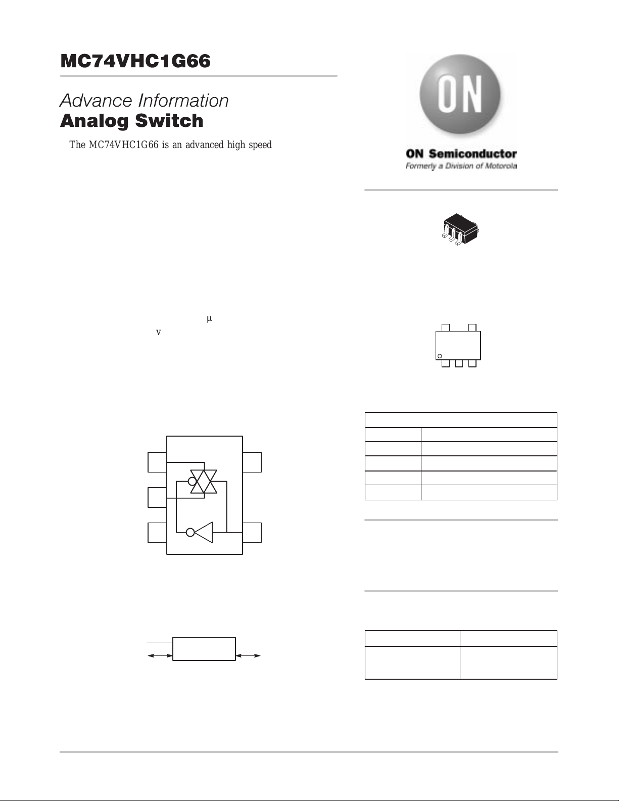
The MC74VHC1G66 is an advanced high speed CMOS bilateral
analog switch fabricated with silicon gate CMOS technology. It
achieves high speed propagation delays and low ON resistances while
maintaining CMOS low power dissipation. This bilateral switch
controls analog and digital voltages that may vary across the full
power–supply range (from VCC to GND).
The MC74VHC1G66 is compatible in function to a single gate of
the High Speed CMOS MC74VHC4066 and the metal–gate CMOS
MC14066. The device has been designed so that the ON resistances
(RON) are much lower and more linear over input voltage than RON of
the metal–gate CMOS or High Speed CMOS analog switches.
The ON/OFF control inputs are compatible with standard CMOS
outputs; with pull–up resistors, it is compatible with LSTTL outputs.
• High Speed: t
• Low Power Dissipation: I
• Diode Protection Provided on Inputs and Outputs
• Improved Linearity and Lower ON Resistance over Input Voltage
than the MC14066 or the HC4066
• Pin and Function Compatible with Other Standard Logic Families
• Latchup Performance Exceeds 300 mA
• ESD Performance: HBM > 2000 V; MM > 200 V, CDM > 1500 V
• Chip Complexity: 11 FETs or 3 Equivalent Gates
= TBD (Typ) at VCC = 5 V
PD
= 2 mA (Max) at TA = 25°C
CC
IN/OUT X
A
OUT/IN Y
2
A
V
51
CC
http://onsemi.com
SC–88A / SOT–353
DF SUFFIX
CASE 419A
MARKING DIAGRAM
d
V9
Pin 1
d = Date Code
PIN ASSIGNMENT
1
2
3 GND
4
5 VCC
IN/OUT X
OUT/IN Y
ON/OFF CONTROL
A
A
ON/OFF CONTROLGND
43
5–Lead SOT–353 Pinout (Top View)
LOGIC SYMBOL
ON/OFF CONTROL
IN/OUT X
A
This document contains information on a new product. Specifications and information
herein are subject to change without notice.
Semiconductor Components Industries, LLC, 1999
November, 1999 – Rev. 1
X 1
1
U U
1
OUT/IN Y
A
1 Publication Order Number:
ORDERING INFORMATION
See detailed ordering and shipping information in the package
dimensions section on page 7 of this data sheet.
FUNCTION TABLE
On/Off Control Input State of Analog Switch
L
H
Off
On
MC74VHC1G66/D
Page 2
MC74VHC1G66
ABSOLUTE MAXIMUM RATINGS
Characteristics Symbol Value Unit
DC Supply Voltage V
Digital Input Voltage V
Analog Output Voltage V
Digital Input Diode Current I
DC Supply Current, VCC and GND I
Power dissipation in still air, SC–88A † P
Lead temperature, 1 mm from case for 10 s T
Storage temperature T
†Derating — SC–88A Package: –3 mW/_C from 65_ to 125_C
CC
IN
IS
IK
CC
D
L
stg
RECOMMENDED OPERATING CONDITIONS
Characteristics Symbol Min Max Unit
DC Supply Voltage V
Digital Input Voltage V
Analog Input Voltage V
Static or Dynamic Voltage Across Switch VIO* 1.2 V
Operating Temperature Range T
Input Rise and Fall Time
ON/OFF Control Input VCC = 3.3V ± 0.3V
VCC = 5.0V ± 0.5V
* For voltage drops across the switch greater than 1.2V (switch on), excessive VCC current may be drawn; i.e. the current out of the switch may
contain both VCC and switch input components. The reliability of the device will be unaffected unless the Maximum Ratings are exceeded.
CC
IN
IS
tr , t
A
f
–0.5 to +7.0 V
–0.5 to VCC +0.5 V
–0.5 to VCC + 0.5 V
–20 mA
+25 mA
200 mW
260 °C
–65 to +150 °C
4.5 5.5 V
GND V
GND V
–55 +85 °C
0
0
CC
CC
100
20
V
V
ns/V
http://onsemi.com
2
Page 3
MC74VHC1G66
V
CC
Î
Î
Î
Î
Î
Î
Î
Î
Î
Î
Î
Î
Î
Î
Î
Î
Î
Î
Î
Î
Î
Î
Î
Î
Î
Î
Î
Î
Î
Î
Î
Î
Î
Î
Î
Î
Î
Î
Î
Î
Î
Î
Î
Î
Î
Î
Î
Î
Î
Î
Î
Î
Î
Î
Î
Î
C
Î
Î
Î
Î
Î
Î
Î
Î
Î
Î
Î
Î
Î
Î
Î
Î
Î
Î
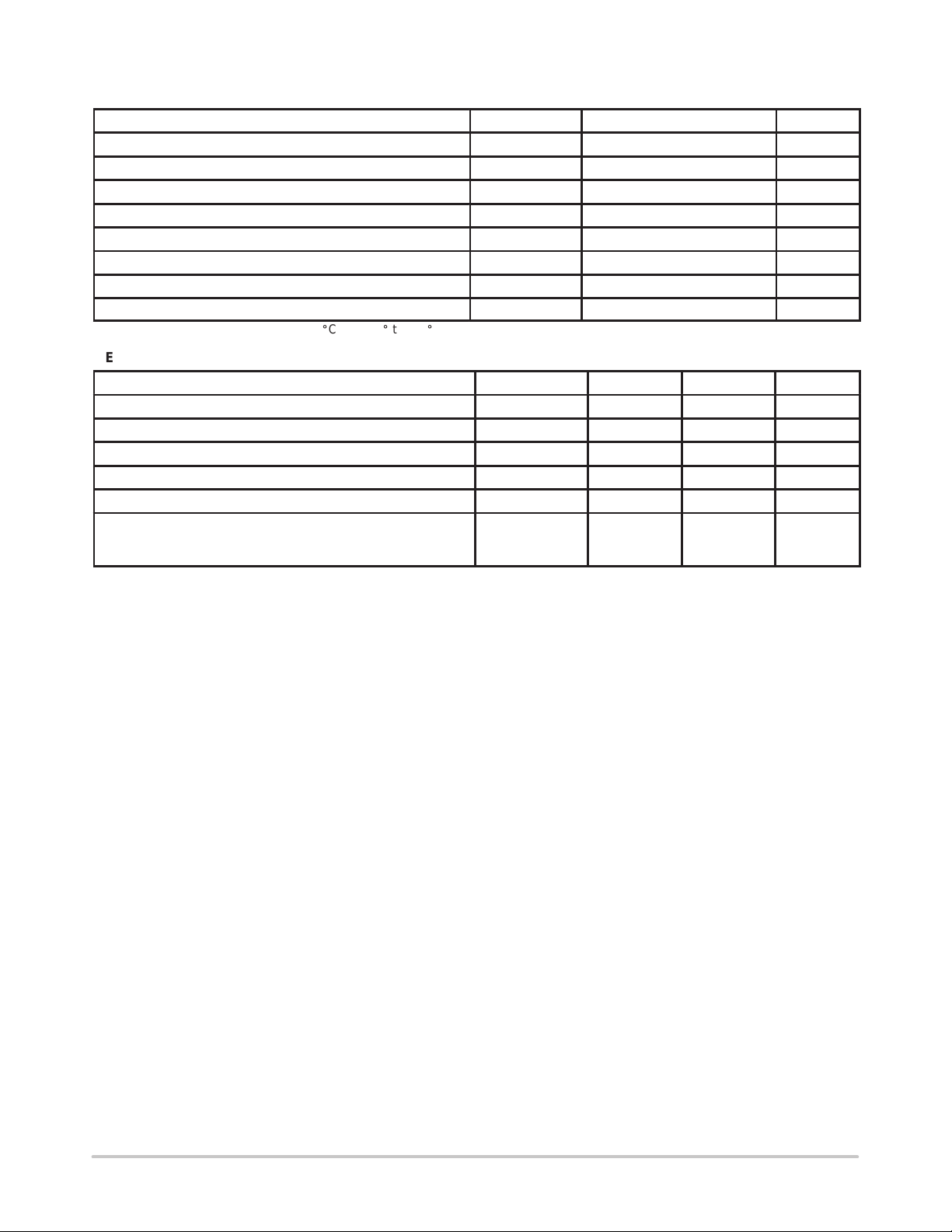
DC ELECTRICAL CHARACTERISTICS
V
CC
Symbol Parameter Test Conditions (V) Min Typ Max Min Max Min Max Unit
V
IH
Minimum High–Level
Input Voltage
ON/OFF Control Input
RON = Per Spec 2.0
3.0
4.5
5.5
V
IL
Maximum Low–Level
Input Voltage
ON/OFF Control Input
RON = Per Spec 2.0
3.0
4.5
5.5
I
IN
Maximum Input
Leakage Current
VIN = VCC or GND 0 to
5.5
ON/OFF Control Input
I
R
CC
ON
Maximum Quiescent
Supply Current
Maximum ”ON”
Resistance
VIN = VCC or GND
VIO = 0V
VIN = V
IH
VIS = VCC or GND
|IIS| ≤ 10mA (Figure 1)
Endpoints
VIN = V
IH
VIS = VCC or GND
5.5 2.0 20 40 µA
3.0
4.5
5.5
3.0
4.5
5.5
|IIS| ≤ 10mA (Figure 1)
I
OFF
Maximum Off–Channel
Leakage Current
VIN = V
IL
VIS = VCC or GND
5.5 0.1 0.5 1.0 µA
Switch Off (Figure 2)
I
ON
Maximum On–Channel
Leakage
Current
VIN = V
IH
VIS = VCC or GND
Switch On (Figure 3)
5.5 0.1 0.5 1.0 µA
TA = 25°C TA ≤ 85°C TA ≤ 125°C
1.5
2.1
3.15
3.85
1.35
1.65
0.5
0.9
1.5
2.1
3.15
3.85
0.5
0.9
1.35
1.65
±0.1 ±1.0 ±1.0 µA
30
20
15
25
12
50
30
20
50
20
8
15
70
40
35
65
26
23
1.5
2.1
3.15
3.85
0.5
0.9
1.35
1.65
100
50
45
90
40
32
V
V
W
W
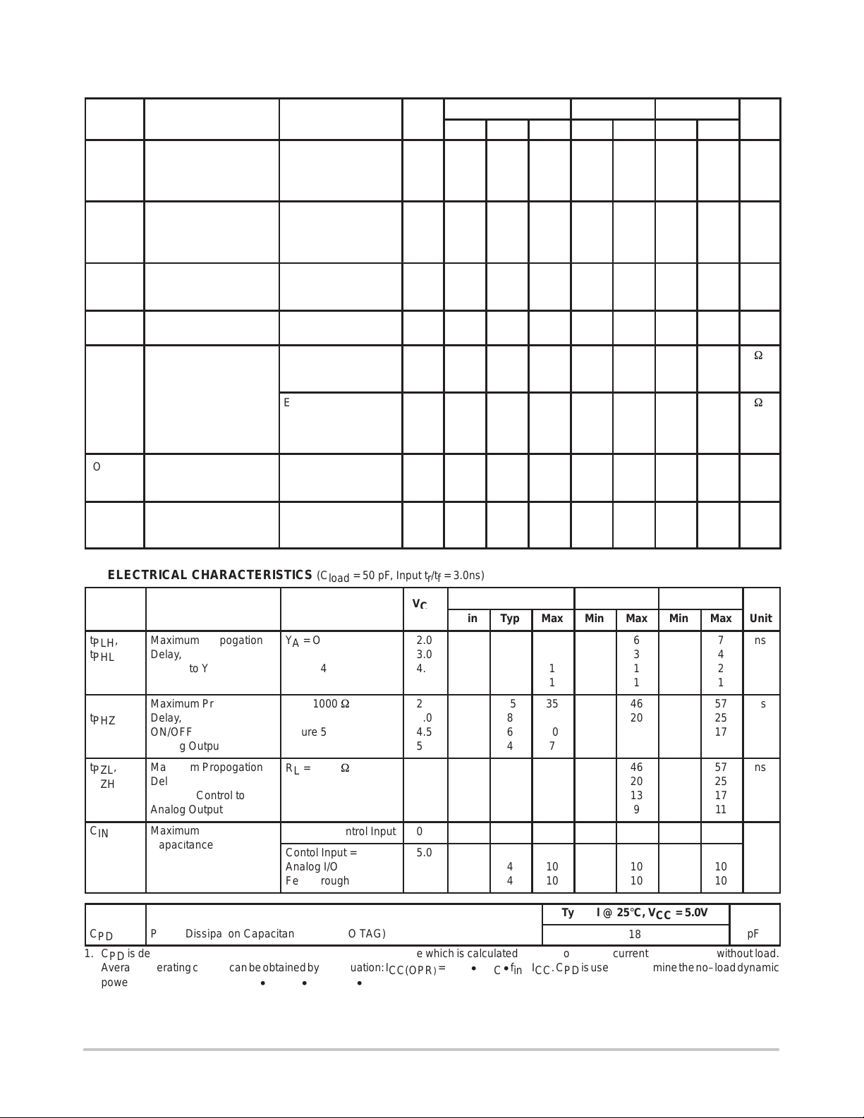
AC ELECTRICAL CHARACTERISTICS (C
Symbol
t
,
PLH
t
PHL
ÎÎ
ÎÎ
t
,
PLZ
t
PHZ
ÎÎ
t
,
PZL
ÎÎ
t
PZH
ÎÎ
C
IN
ÎÎ
ÎÎ
Parameter
Maximum Propogation
Delay,
ООООО
Input X to Y
ООООО
Maximum Propogation
Delay,
ON/OFF Control to
ООООО
Analog Output
Maximum Propogation
ООООО
Delay,
ON/OFF Control to
ООООО
Analog Output
Maximum Input
apacitance
ООООО
ООООО
Test Conditions
YA = Open
ООООО
Figure 4
ООООО
RL = 1000
Figure 5
ООООО
RL = 1000
ООООО
Figure 5
ООООО
ON/OFF Control Input
Contol Input = GND
ООООО
Analog I/O
Feedthrough
ООООО
= 50 pF, Input tr/tf = 3.0ns)
load
V
(V)
2.0
3.0
Î
4.5
5.5
Î
W
2.0
3.0
4.5
Î
5.5
W
2.0
Î
3.0
4.5
Î
5.5
0.0
5.0
Î
Î
TA = 25°C
Min
Typ
1
0
Î
Î
Î
0
0
Î
15
8
ÎÎÎ
6
4
Î
Î
15
Î
8
6
Î
4
3
Î
Î
Î
4
4
Î
Max
5
2
Î
1
1
Î
35
15
10
Î
7
35
Î
15
10
Î
7
10
Î
10
10
Î
TA ≤ 85°C
Min
Max
6
3
Î
Î
Î
1
1
Î
46
20
ÎÎÎ
13
9
Î
Î
46
Î
20
13
Î
9
10
Î
Î
Î
10
10
Î
TA ≤ 125°C
Min
Max
7
4
Î
Î
Î
2
1
Î
57
25
ÎÎÎ
17
11
Î
Î
57
Î
25
17
Î
11
10
Î
Î
Î
10
10
Î
Unit
ns
ns
ns
pF
Typical @ 25°C, VCC = 5.0V
C
PD
Power Dissipation Capacitance (Note NO T AG)
18
pF
1. CPD is defined as the value of the internal equivalent capacitance which is calculated from the operating current consumption without load.
Average operating current can be obtained by the equation: I
2
power consumption; PD = CPD V
fin + ICC VCC.
CC
CC(OPR
= CPD VCC fin + ICC. CPD is used to determine the no–load dynamic
)
http://onsemi.com
3
Page 4
MC74VHC1G66
Î
Î
Î
Î
Î
Î
Î
Î
Î
Î
Î
Î
Î
Î
Î
Î
Î
Î
Î
Î
Î
Î
Î
Î
Î
Î
Î
Î
Î
Î
Î
Î
Î
Î
Î
Î
Î
Î
Î
Î
Î
Î
Î
Î
Î
Î
Î
Î
Î
Î
Î
Î
Î
Î
Î
Î
Î
Î
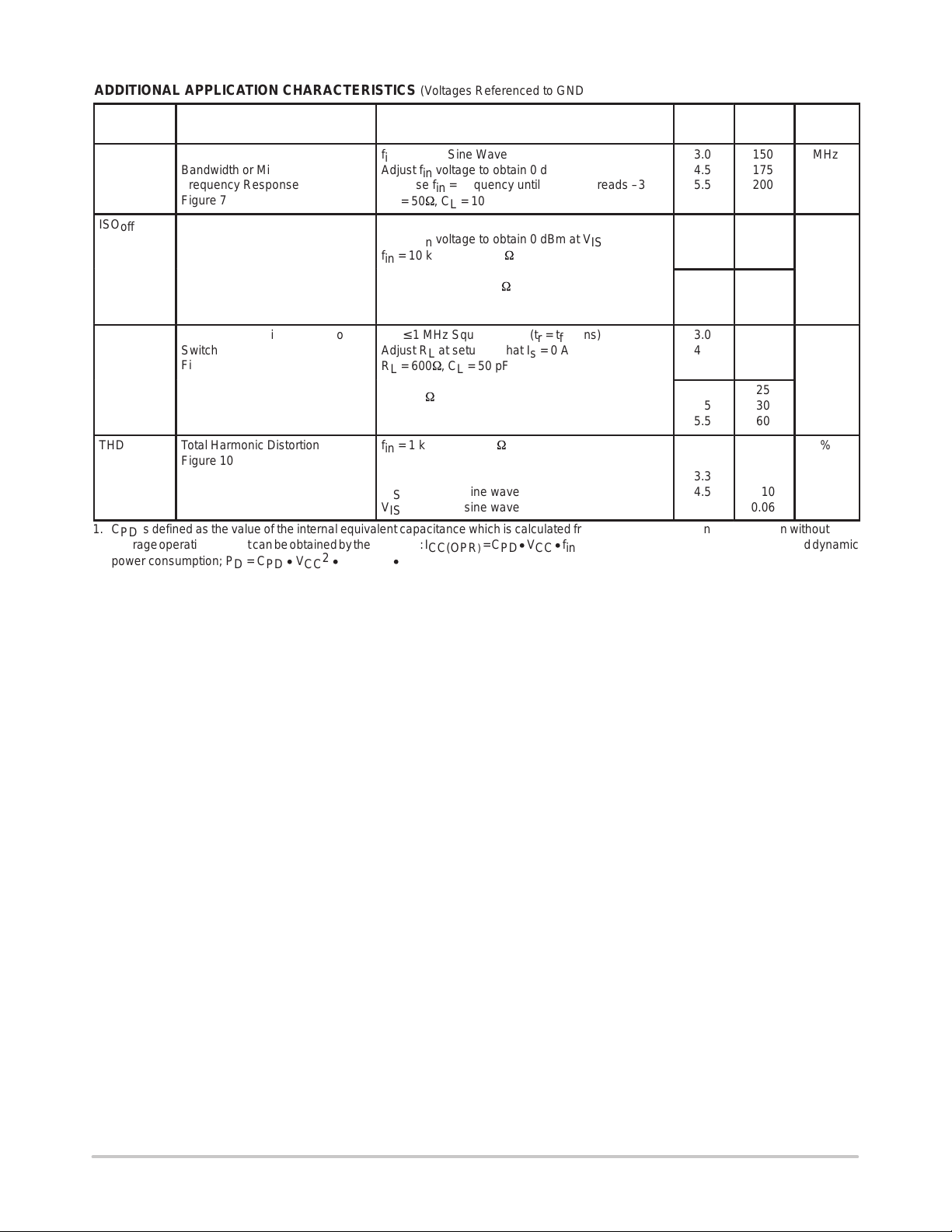
ADDITIONAL APPLICATION CHARACTERISTICS (Voltages Referenced to GND Unless Noted)
Limit
Symbol
ÎÎÎ
BW
ООООООО
Maximum On–Channel
Bandwidth or Minimum
ÎÎÎ
Frequency Response
ООООООО
Figure 7
ISO
off
ÎÎÎ
ÎÎÎ
ÎÎÎÎОООООООÎОООООООООООО
NOISE
ÎÎÎ
ÎÎÎ
ÎÎÎ
THD
ÎÎÎ
ÎÎÎ
Off–Channel Feedthrough
ООООООО
Isolation
Figure 8
ООООООО
Feedthrough Noise Control to
feed
Switch
ООООООО
Figure 9
ООООООО
ООООООО
Total Harmonic Distortion
Figure 10
ООООООО
ООООООО
Parameter
ОООООООООООО
Test Conditions
fin = 1 MHz Sine Wave
Adjust fin voltage to obtain 0 dBm at V
Increase fin = frequency until dB meter reads –3dB
ОООООООООООО
OS
RL = 50W, CL = 10 pF
fin = Sine Wave
ОООООООООООО
Adjust fin voltage to obtain 0 dBm at V
fin = 10 kHz, RL = 600W, CL = 50 pF
ОООООООООООО
IS
fin = 1.0 kHz, RL = 50W, CL = 10 pF
Vin ≤ 1 MHz Square Wave (tr = tf = 2ns)
Adjust RL at setup so that Is = 0 A
ОООООООООООО
RL = 600W, CL = 50 pF
RL = 50W, CL = 10 pF
ОООООООООООО
ОООООООООООО
fin = 1 kHz, RL = 10kW, CL = 50 pF
THD = THD
ОООООООООООО
VIS = 3.0 VPP sine wave
VIS = 4.0 VPP sine wave
ОООООООООООО
VIS = 5.0 VPP sine wave
Measured
– THD
Source
V
Î
3.0
4.5
5.5
Î
3.0
Î
4.5
5.5
Î
3.0
4.5
Î
5.5
3.0
4.5
Î
5.5
3.0
Î
4.5
5.5
Î
Î
3.3
4.5
Î
5.5
CC
1. CPD is defined as the value of the internal equivalent capacitance which is calculated from the operating current consumption without load.
Average operating current can be obtained by the equation: I
2
power consumption; PD = CPD V
fin + ICC VCC.
CC
CC(OPR
= CPD VCC fin + ICC. CPD is used to determine the no–load dynamic
)
25°C
ÎÎ
150
175
200
ÎÎ
–50
ÎÎ
–50
–50
ÎÎ
–40
–40
ÎÎ
–40
45
60
ÎÎ
130
25
ÎÎ
30
60
ÎÎ
ÎÎ
0.20
0.10
ÎÎ
0.06
Unit
Î
MHz
Î
Î
Î
Î
mV
Î
Î
Î
Î
Î
dB
PP
%
http://onsemi.com
4
Page 5

PLOTTER
MC74VHC1G66
POWER
SUPPLY
COMPUTER
+–
2
51
43
DC PARAMETER
ANALYZER
V
CC
V
CC
51
V
CC
A
2
43
Figure 1. On Resistance T est Set–Up Figure 2. Maximum Off–Channel Leakage Current
T est Set–Up
V
CC
N/C
A
2
51
43
V
CC
51
V
IH
TEST
POINT
2
43
V
CC
V
IL
V
CC
V
CC
Figure 3. Maximum On–Channel Leakage Current
T est Set–Up
Switch to Position 1 when testing t
Switch to Position 2 when testing t
V
CC
1
2
V
CC
1
2
TEST POINT
R
L
CL*
2
*Includes all probe and jig capacitance.
PLZ
PHZ
and t
and t
51
43
PZL
PZH
Figure 5. Propagation Delay Output Enable/Disable
T est Set–Up
Figure 4. Propagation Delay T est Set–Up
V
CC
V
CC
N/C
N/C
51
2
43
A
Figure 6. Power Dissipation Capacitance T est
Set–Up
http://onsemi.com
5
Page 6

MC74VHC1G66
V
OS
0.1 mF
f
in
2
dB
Meter
CL*
*Includes all probe and jig capacitance.
51
43
Figure 7. Maximum On–Channel Bandwidth
T est Set–Up
(VCC)/2
R
R
L
V
OS
CL*
L
51
2
I
S
43
*Includes all probe and jig capacitance.
V
V
CC
f
in
dB
Meter
0.1 mF
R
L
V
IS
CL*
OS
51
2
43
*Includes all probe and jig capacitance.
V
CC
Figure 8. Off–Channel Feedthrough Isolation T est
Set–Up
T o Distortion
Meter
(VCC)/2
V
CC
R
L
f
V
v
1MHz
IN
+
tf+
t
r
2ns
V
CC
GND
V
OS
CL*
in
V
IS
0.1 mF
2
*Includes all probe and jig capacitance.
V
CC
51
43
Figure 9. Feedthrough Noise, ON/OFF Control to
Analog Out, Test Set–Up
V
X
A
50%
t
PLH
Y
A
50% V
CC
50% V
CC
t
PHL
CC
V
OH
V
OL
Figure 11. Propagation Delay,
Analog In to Analog Out Waveforms
Figure 10. Total Harmonic Distortion Test Set–Up
Control
50% V
Analog Out
50% V
t
r
90%
10%
t
t
PZL
CC
CC
PZH
t
f
V
50% V
t
PLZ
t
PHZ
CC
10%
90%
CC
High
Impedance
V
OL
V
OH
High
Impedance
Figure 12. Propagation Delay , ON/OFF Control
http://onsemi.com
6
Page 7

MC74VHC1G66
DEVICE ORDERING INFORMATION
Device Nomenclature
Temp
Device Order Number
Circuit
Indicator
Range
Identifier
Technology
Device
Function
Package
Suffix
MC74VHC1G66DFT1 MC 74 VHC1G 66 DF T1
P ACKAGE DIMENSIONS
SC–88A / SOT–353
DF SUFFIX
5–LEAD PACKAGE
CASE 419A–01
ISSUE B
S
123
A
G
V
45
–B–
MM
D 5 PL
B0.2 (0.008)
N
NOTES:
1. DIMENSIONING AND TOLERANCING PER ANSI
2. CONTROLLING DIMENSION: MM.
0.5 mm (min)
Tape &
Reel
Suffix
Y14.5M, 1982.
DIMAMIN MAX MIN MAX
B 1.15 1.350.045 0.053
C 0.80 1.100.031 0.043
D 0.10 0.300.004 0.012
G 0.65 BSC0.026 BSC
H ––– 0.10–––0.004
J 0.10 0.250.004 0.010
K 0.10 0.300.004 0.012
N 0.20 REF0.008 REF
S 2.00 2.200.079 0.087
V 0.30 0.400.012 0.016
INCHES
Package
Type
SC–88A /
SOT–353
MILLIMETERS
1.80 2.200.071 0.087
Tape and Reel
Size
7–Inch/3000 Unit
J
C
H
K
0.65 mm 0.65 mm
0.4 mm (min)
1.9 mm
http://onsemi.com
7
Page 8

K
t
COVER
B
1
FOR MACHINE REFERENCE
INCLUDING DRAFT AND RADII
CONCENTRIC AROUND B
ONLY
R MIN.
K
0
SEE
NOTE 2
0
TOP
TAPE
MC74VHC1G66
D
EMBOSSMENT
USER DIRECTION OF FEED
P
SEE NOTE 2A
0
B
0
P
10 PITCHES
CUMULATIVE
TOLERANCE ON
P
0
2
TAPE
±0.2 mm
(±0.008”)
E
F
W
++ +
D
1
FOR COMPONENTS
CENTER LINES
OF CAVITY
2.0 mm × 1.2 mm
AND LARGER
*TOP COVER
TAPE THICKNESS (t1)
0.10 mm
(0.004”) MAX.
TAPE AND COMPONENTS
BENDING RADIUS
10°
MAXIMUM COMPONENT ROTATION
SHALL PASS AROUND RADIUS “R”
WITHOUT DAMAGE
TYPICAL
COMPONENT CAVITY
CENTER LINE
TYPICAL
COMPONENT
CENTER LINE
ALLOWABLE CAMBER TO BE 1 mm/100 mm NONACCUMULATIVE OVER 250
EMBOSSED
CARRIER
100 mm
(3.937”)
1 mm MAX
CAMBER (TOP VIEW)
1 mm
(0.039”) MAX
EMBOSSMENT
TAPE
250 mm
(9.843”)
mm
Figure 13. Carrier Tape Specifications
EMBOSSED CARRIER DIMENSIONS (See Notes 1 and 2)
Tape
Size
8 mm 4.35 mm
1. Metric Dimensions Govern–English are in parentheses for reference only.
2. A0, B0, and K0 are determined by component size. The clearance between the components and the cavity must be within 0.05 mm min to
B
1
Max
(0.171”)
0.50 mm max. The component cannot rotate more than 10° within the determined cavity
D D
1.5 +0.1/
–0.0 mm
(0.059
+0.004/
–0.0”)
1
1.0 mm
Min
(0.039”)
E F K P P
1.75
±0.1 mm
(0.069
±0.004”)
3.5
±0.5 mm
(1.38
±0.002”)
2.4 mm
(0.094”)
4.0
±0.10 mm
(0.157
±0.004”)
0
4.0
±0.1 mm
(0.156
±0.004”)
P
2
2.0
±0.1 mm
(0.079
±0.002”)
R T W
25 mm
(0.98”)
0.3
±0.05 mm
(0.01
+0.0038/
–0.0002”)
8.0
±0.3 mm
(0.315
±0.012”)
http://onsemi.com
8
Page 9

MC74VHC1G66
13.0 mm ±0.2 mm
1.5 mm MIN
(0.06”)
(0.512” ±0.008”)
t MAX
20.2 mm MIN
A
(0.795”)
REEL DIMENSIONS
Tape
Size
8 mm 330 mm
FULL RADIUS
Figure 14. Reel Dimensions
A Max G t Max
(13”)
DIRECTION OF FEED
8.400 mm, +1.5 mm, –0.0
(0.33”, +0.059”, –0.00)
14.4 mm
(0.56”)
50 mm MIN
(1.969”)
G
BARCODE LABEL
Figure 15. Reel Winding Direction
http://onsemi.com
9
HOLEPOCKET
Page 10

MC74VHC1G66
CAVITY
TAPE
TOP TAPE
TAPE TRAILER
(Connected to Reel Hub)
NO COMPONENTS
160 mm MIN
Figure 16. T ape Ends for Finished Goods
“T1” PIN ONE TOWARDS
SPROCKET HOLE
COMPONENTS
DIRECTION OF FEED
SC–88A/SOT–353 (5 Pin)
DEVICE
User Direction of Feed
Figure 17. Reel Configuration
TAPE LEADER
NO COMPONENTS
400 mm MIN
http://onsemi.com
10
Page 11

Notes
MC74VHC1G66
http://onsemi.com
11
Page 12

MC74VHC1G66
ON Semiconductor and are trademarks of Semiconductor Components Industries, LLC (SCILLC). SCILLC reserves the right to make changes
without further notice to any products herein. SCILLC makes no warranty , representation or guarantee regarding the suitability of its products for any particular
purpose, nor does SCILLC assume any liability arising out of the application or use of any product or circuit, and specifically disclaims any and all liability ,
including without limitation special, consequential or incidental damages. “Typical” parameters which may be provided in SCILLC data sheets and/or
specifications can and do vary in different applications and actual performance may vary over time. All operating parameters, including “Typicals” must be
validated for each customer application by customer’s technical experts. SCILLC does not convey any license under its patent rights nor the rights of others.
SCILLC products are not designed, intended, or authorized for use as components in systems intended for surgical implant into the body, or other applications
intended to support or sustain life, or for any other application in which the failure of the SCILLC product could create a situation where personal injury or
death may occur. Should Buyer purchase or use SCILLC products for any such unintended or unauthorized application, Buyer shall indemnify and hold
SCILLC and its officers, employees, subsidiaries, affiliates, and distributors harmless against all claims, costs, damages, and expenses, and reasonable
attorney fees arising out of, directly or indirectly , any claim of personal injury or death associated with such unintended or unauthorized use, even if such claim
alleges that SCILLC was negligent regarding the design or manufacture of the part. SCILLC is an Equal Opportunity/Affirmative Action Employer .
PUBLICATION ORDERING INFORMATION
USA/EUROPE Literature Fulfillment:
Literature Distribution Center for ON Semiconductor
P.O. Box 5163, Denver, Colorado 80217 USA
Phone: 303–675–2175 or 800–344–3860 Toll Free USA/Canada
Fax: 303–675–2176 or 800–344–3867 Toll Free USA/Canada
Email: ONlit@hibbertco.com
Fax Response Line*: 303–675–2167
800–344–3810 Toll Free USA/Canada
*To receive a Fax of our publications
N. America Technical Support: 800–282–9855 Toll Free USA/Canada
http://onsemi.com
ASIA/PACIFIC: LDC for ON Semiconductor – Asia Support
Phone: 303–675–2121 (Tue–Fri 9:00am to 1:00pm, Hong Kong Time)
Email: ONlit–asia@hibbertco.com
JAPAN: ON Semiconductor, Japan Customer Focus Center
4–32–1 Nishi–Gotanda, Shinagawa–ku, T okyo, Japan 141–8549
Phone: 81–3–5487–8345
Email: r14153@onsemi.com
ON Semiconductor Website: http://onsemi.com
For additional information, please contact your local Sales Representative.
MC74VHC1G66/D
12
 Loading...