

Page 1
MC74VHC1G09
2−Input AND Gate with
Open Drain Output
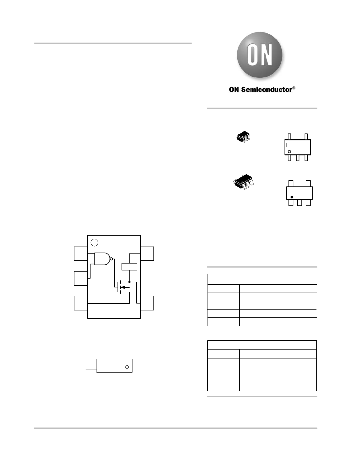
The MC74VHC1G09 is a n advanced h igh s peed C MOS 2 −input AND
gate with open drain output fabricated with silicon gate CMOS
technology . It achieves high speed operation similar to equivalent Bipol ar
Schottky TTL while maintaining CMOS low power dissipation.
The internal circuit is composed of three stages, including an open
drain output which provid es the capability to set output switching level.
This allows the MC74VHC1G09 to be used to interface 5 V circuits to
circuits of any voltage between VCC and 7 V using an external resistor
and power supply.
The MC74VHC1G09 input structure provides protection when
voltages up to 7 V are applied, regardless of the supply voltage.
Features
• High Speed: t
• Low Internal Power Dissipation: I
• Power Down Protection Provided on Inputs
• Pin and Function Compatible with Other Standard Logic Families
• Chip Complexity: FETs = 62; Equivalent Gates = 16
• Pb−Free Packages are Available
= 4.3 ns (Typ) at VCC = 5 V
PD
= 1 mA (Max) at TA = 25°C
CC
http://onsemi.com
SC−88A / SOT−353 / SC−70
DF SUFFIX
CASE 419A
TSOP−5 / SOT−23 / SC−59
DT SUFFIX
CASE 483
MARKING
DIAGRAMS
5
M
VX M G
G
1
VX M G
G
IN B
IN A
GND
1
OVT
2
3
Figure 1. Pinout (Top View)
IN A
IN B
&
Figure 2. Logic Symbol
5
4
OUT Y
V
CC
OUT Y
VX = Device Code
M = Date Code*
G = Pb−Free Package
(Note: Microdot may be in either location)
*Date Code orientation and/or position may
vary depending upon manufacturing location.
PIN ASSIGNMENT
1
2
3 GND
4
5V
IN B
IN A
OUT Y
CC
FUNCTION TABLE
Inputs Output
AB
L
L
H
H
L
H
L
H
Y
L
L
L
Z
© Semiconductor Components Industries, LLC, 2007
January, 2007 − Rev. 16
ORDERING INFORMATION
See detailed ordering and shipping information in the package
dimensions section on page 4 of this data sheet.
1 Publication Order Number:
MC74VHC1G09/D
Page 2
MC74VHC1G09
MAXIMUM RATINGS
Symbol Characteristics Value Unit
V
V
V
OUT
I
I
OK
I
OUT
I
CC
P
q
T
T
T
MSL Moisture Sensitivity Level 1
F
V
ESD
I
Latchup
Stresses exceeding Maximum Ratings may damage the device. Maximum Ratings are stress ratings only. Functional operation above the
Recommended Operating Conditions is not implied. Extended exposure to stresses above the Recommended Operating Conditions may affect
device reliability.
1. Tested to EIA/JESD22−A114−A
2. Tested to EIA/JESD22−A115−A
3. Tested to JESD22−C101−A
4. Tested to EIA/JESD78
DC Supply Voltage −0.5 to +7.0 V
CC
DC Input Voltage −0.5 to +7.0 V
IN
DC Output Voltage −0.5 to 7.0 V
Input Diode Current −20 mA
IK
Output Diode Current +20 mA
DC Output Current, per Pin +25 mA
DC Supply Current, VCC and GND +50 mA
Power dissipation in still air SC−88A, TSOP−5 200 mW
D
Thermal resistance SC−88A, TSOP−5 333 °C/W
JA
Lead temperature, 1 mm from case for 10 s 260 °C
L
Junction temperature under bias +150 °C
J
Storage temperature −65 to +150 °C
stg
Flammability Rating Oxygen Index: 28 to 34 UL 94 V−0 @ 0.125 in
R
ESD Withstand Voltage Human Body Model (Note 1)
Machine Model (Note 2)
Charged Device Model (Note 3)
> 2000
> 200
N/A
Latchup Performance Above VCC and Below GND at 125°C (Note 4) ±500 mA
V
RECOMMENDED OPERATING CONDITIONS
Symbol Characteristics Min Max Unit
V
V
V
OUT
T
tr, t
DC Supply Voltage 2.0 5.5 V
CC
DC Input Voltage 0.0 5.5 V
IN
DC Output Voltage 0.0 7.0 V
Operating Temperature Range −55 +125 °C
A
Input Rise and Fall Time VCC = 3.3 V ± 0.3 V
f
VCC = 5.0 V ± 0.5 V
0
0
100
20
Device Junction Temperature versus
Time to 0.1% Bond Failures
Junction
Temperature °C
Time, Hours Time, Years
80 1,032,200 117.8
90 419,300 47.9
100 178,700 20.4
110 79,600 9.4
120 37,000 4.2
130 17,800 2.0
140 8,900 1.0
FAILURE RATE OF PLASTIC = CERAMIC
UNTIL INTERMETALLICS OCCUR
= 130 C°
J
T
J
J
T
T
= 110 C°
= 120 C°
1
NORMALIZED FAILURE RATE
1 10 100
TIME, YEARS
C°
C°
= 80
= 90
= 100 C°
J
T
J
J
T
T
Figure 3. Failure Rate vs. Time
Junction Temperature
ns/V
1000
http://onsemi.com
2
Page 3
DC ELECTRICAL CHARACTERISTICS
l
Î
Î
Î
ÎÎ
ÎÎ
Î
Î
Î
Î
Î
Î
Î
Î
Î
Î
ÎÎ
ÎÎ
ÎÎ
ÎÎ
Î
Î
Î
Î
Î
Î
Î
Î
ÎÎ
ÎÎ
ÎÎ
Î
Î
Î
Î
Î
Î
Î
Î
Î
ÎÎ
ÎÎ
Symbol Parameter Test Conditions
V
V
V
I
I
CC
I
OFF
Minimum High−Level
IH
Input Voltage
Maximum Low−Level
IL
Input Voltage
Maximum Low−Leve
OL
Output Voltage
VIN = VIH or V
Maximum Input
IN
Leakage Current
Maximum Quiescent
Supply Current
Power Off−Output
Leakage Current
VIN = VIH or V
IOL = 50 mA
IL
IL
VIN = VIH or V
IOL = 4 mA
IL
IOL = 8 mA
VIN = 5.5 V or GND 0 to
VIN = VCC or GND 5.5 1.0 20 40
V
= 5.5 V
OUT
VIN = 5.5 V
MC74VHC1G09
V
CC
(V)
2.0
3.0
4.5
5.5
2.0
3.0
4.5
5.5
2.0
3.0
4.5
3.0
4.5
5.5
0 0.25 2.5 5
TA = 25°C TA ≤ 85°C −55 ≤ TA ≤ 125°C
Min Typ Max Min Max Min Max
1.5
2.1
3.15
3.85
1.35
1.65
0.0
0.0
0.0
0.36
0.36
0.5
0.9
0.1
0.1
0.1
1.5
2.1
3.15
3.85
1.5
2.1
3.15
3.85
0.5
0.9
1.35
1.65
0.1
0.1
0.1
0.44
0.44
±0.1 ±1.0 ±1.0
0.5
0.9
1.35
1.65
0.1
0.1
0.1
0.52
0.52
Unit
V
V
V
V
mA
mA
mA
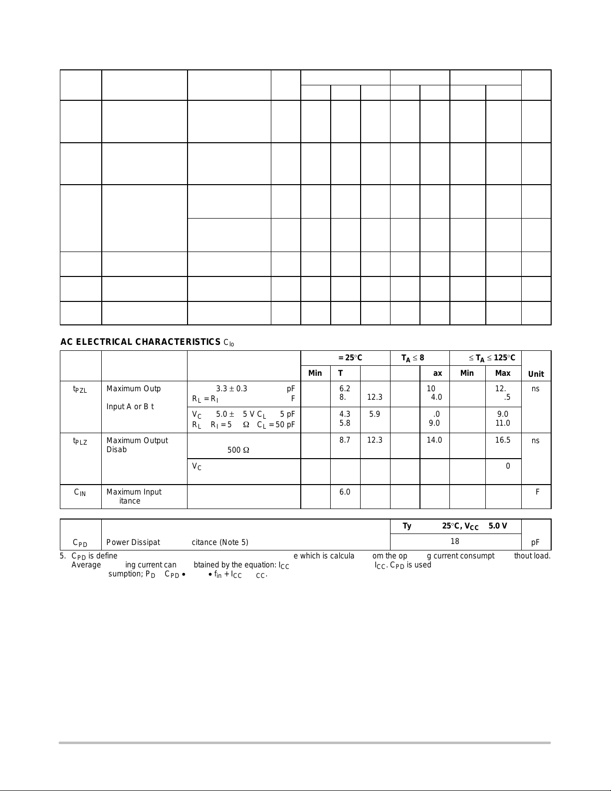
AC ELECTRICAL CHARACTERISTICS C
ÎÎ
Symbol
t
PZL
ÎÎ
ÎÎ
ÎÎ
t
PLZ
ÎÎ
ÎÎ
C
ÎÎ
ООООО
Maximum Output
ООООО
Enable Time,
Input A or B to Y
ООООО
ООООО
Maximum Output
Disable Time
ООООО
ООООО
Maximum Input Ca-
IN
pacitance
ООООО
Parameter
ОООООО
Test Conditions
VCC = 3.3 ± 0.3 V CL = 15 pF
ОООООО
RL = RI = 500 W CL = 50 pF
VCC = 5.0 ± 0.5 V CL = 15 pF
RL = RI = 500 W CL = 50 pF
ОООООО
VCC = 3.3 ± 0.3 V CL = 50 pF
RL = RI = 500 W
VCC = 5.0 ± 0.5 V CL = 50 pF
ОООООО
RL = RI = 500 W
ООООООÎÎÎÎ
= 50 pF, Input tr = t
load
= 3.0 ns
f
TA = 25°C
Min
Typ
ÎÎÎ
6.2
8.7
4.3
ÎÎÎ
5.8
8.7
ÎÎÎ
5.8
6.0
Max
8.8
Î
12.3
5.9
7.9
Î
12.3
7.9
Î
10
Î
TA ≤ 85°C
Min
Max
10.5
ÎÎÎ
14.0
7.0
ÎÎÎ
9.0
14.0
ÎÎÎ
9.0
10
ÎÎÎ
−55 ≤ TA ≤ 125°C
Min
ÎÎÎÎ
Max
12.5
16.5
9.0
ÎÎÎÎ
11.0
16.5
ÎÎÎÎ
11.0
10
ÎÎÎÎ
Unit
ns
ns
pF
Typical @ 25°C, VCC = 5.0 V
C
Power Dissipation Capacitance (Note 5)
PD
18
pF
5. CPD is defined as the value of the internal equivalent capacitance which is calculated from the operating current consumption without load.
Average operating current can be obtained by the equation: I
power consumption; PD = CPD V
2
fin + ICC VCC.
CC
= CPD VCC fin + ICC. CPD is used to determine the no−load dynamic
)
CC(OPR
http://onsemi.com
3
Page 4

MC74VHC1G09
VCC − 7 V
L
V
CC
A
OVT
R
L
B
Figure 4. Output Voltage Mismatch Application Figure 5. Switching Waveforms
A or B
50%
t
t
PLZ
PZL
Y
V
CC
50% V
CC
VOL +0.3 V
V
CC
GND
HIGH
IMPEDANCE
PULSE
GENERATOR
DUT
R
T
= 50 pF equivalent (Includes jig and probe capacitance)
C
L
R
1
C
R
L
L
VCC x 2
RL = R1 = 500 W or equivalent
MC74VHC1G09
A
B
V
CC
RT = Z
2.2 kW
of pulse generator (typically 50 W)
OUT
Figure 6. Test Circuit
1
B
A
5
2
V
CCVCC
MC74VHC1G09
R
LED
3.3 V 1.5 V
MC74VHC1G03
4
C
D
E = (A • B) + (C+D)
3
A
B
Figure 7. Complex Boolean Functions Figure 8. LED Driver Figure 9. GTL Driver
220 W
GT
ORDERING INFORMATION
Device Package Shipping
MC74VHC1G09DFT1 SC70−5 / SC−88A / SOT−353
MC74VHC1G09DFT1G SC70−5 / SC−88A / SOT−353
(Pb−Free)
MC74VHC1G09DFT2 SC70−5 / SC−88A / SOT−353
MC74VHC1G09DFT2G SC70−5 / SC−88A / SOT−353
3000/Tape & Reel
(Pb−Free)
MC74VHC1G09DTT1 SOT23−5 / TSSOP−5 / SC59−5
MC74VHC1G09DTT1G SOT23−5 / TSSOP−5 / SC59−5
(Pb−Free)
†For information on tape and reel specifications, including part orientation and tape sizes, please refer to our Tape and Reel Packaging
Specifications Brochure, BRD8011/D.
†
http://onsemi.com
4
Page 5

MC74VHC1G09
PACKAGE DIMENSIONS
SC−88A, SOT−353, SC−70
CASE 419A−02
ISSUE J
A
G
45
D 5 PL
−B−
MM
B0.2 (0.008)
S
12 3
N
NOTES:
1. DIMENSIONING AND TOLERANCING
PER ANSI Y14.5M, 1982.
2. CONTROLLING DIMENSION: INCH.
3. 419A−01 OBSOLETE. NEW STANDARD
419A−02.
4. DIMENSIONS A AND B DO NOT INCLUDE
MOLD FLASH, PROTRUSIONS, OR GATE
BURRS.
INCHES
DIMAMIN MAX MIN MAX
B 1.15 1.350.045 0.053
C 0.80 1.100.031 0.043
D 0.10 0.300.004 0.012
G 0.65 BSC0.026 BSC
H −−− 0.10−−−0.004
J 0.10 0.250.004 0.010
K 0.10 0.300.004 0.012
N 0.20 REF0.008 REF
S 2.00 2.200.079 0.087
MILLIMETERS
1.80 2.200.071 0.087
J
C
H
K
SOLDERING FOOTPRINT*
0.50
0.0197
0.65
0.025
0.65
0.025
0.40
0.0157
1.9
0.0748
SCALE 20:1
ǒ
inches
mm
*For additional information on our Pb−Free strategy and soldering
details, please download the ON Semiconductor Soldering and
Mounting Techniques Reference Manual, SOLDERRM/D.
http://onsemi.com
5
Ǔ
Page 6

MC74VHC1G09
PACKAGE DIMENSIONS
TSOP−5
CASE 483−02
ISSUE F
NOTES:
1. DIMENSIONING AND TOLERANCING PER
NOTE 5
2X
2X
T0.10
T0.20
54
123
L
G
D
0.205XC AB
M
S
B
K
DETAIL Z
A
J
DETAIL Z
C
0.05
H
SEATING
PLANE
T
ASME Y14.5M, 1994.
2. CONTROLLING DIMENSION: MILLIMETERS.
3. MAXIMUM LEAD THICKNESS INCLUDES
LEAD FINISH THICKNESS. MINIMUM LEAD
THICKNESS IS THE MINIMUM THICKNESS
OF BASE MATERIAL.
4. DIMENSIONS A AND B DO NOT INCLUDE
MOLD FLASH, PROTRUSIONS, OR GATE
BURRS.
5. OPTIONAL CONSTRUCTION: AN
ADDITIONAL TRIMMED LEAD IS ALLOWED
IN THIS LOCATION. TRIMMED LEAD NOT TO
EXTEND MORE THAN 0.2 FROM BODY.
MILLIMETERS
DIM MIN MAX
A 3.00 BSC
B 1.50 BSC
C 0.90 1.10
D 0.25 0.50
G 0.95 BSC
H 0.01 0.10
J 0.10 0.26
K 0.20 0.60
L 1.25 1.55
M 0 10
__
S 2.50 3.00
SOLDERING FOOTPRINT*
1.9
0.95
0.037
1.0
0.039
*For additional information on our Pb−Free strategy and soldering
details, please download the ON Semiconductor Soldering and
Mounting Techniques Reference Manual, SOLDERRM/D.
ON Semiconductor and are registered trademarks of Semiconductor Components Industries, LLC (SCILLC). SCILLC reserves the right to make changes without further notice
to any products herein. SCILLC makes no warranty, representation or guarantee regarding the suitability of its products for any particular purpose, nor does SCILLC assume any liability
arising out of the application or use of any product or circuit, and specifically disclaims any and all liability, including without limitation special, consequential or incidental damages.
“Typical” parameters which may be provided in SCILLC data sheets and/or specifications can and do vary in different applications and actual performance may vary over time. All
operating parameters, including “Typicals” must be validated for each customer application by customer’s technical experts. SCILLC does not convey any license under its patent rights
nor the rights of others. SCILLC products are not designed, intended, or authorized for use as components in systems intended for surgical implant into the body, or other applications
intended to support or sustain life, or for any other application in which the failure of the SCILLC product could create a situation where personal injury or death may occur. Should
Buyer purchase or use SCILLC products for any such unintended or unauthorized application, Buyer shall indemnify and hold SCILLC and its officers, employees, subsidiaries, affiliates,
and distributors harmless against all claims, costs, damages, and expenses, and reasonable attorney fees arising out of, directly or indirectly, any claim of personal injury or death
associated with such unintended or unauthorized use, even if such claim alleges that SCILLC was negligent regarding the design or manufacture of the part. SCILLC is an Equal
Opportunity/Affirmative Action Employer. This literature is subject to all applicable copyright laws and is not for resale in any manner.
0.074
0.028
0.7
2.4
0.094
SCALE 10:1
ǒ
inches
mm
Ǔ
PUBLICATION ORDERING INFORMATION
LITERATURE FULFILLMENT:
Literature Distribution Center for ON Semiconductor
P.O. Box 5163, Denver, Colorado 80217 USA
Phone: 303−675−2175 or 800−344−3860 Toll Free USA/Canada
Fax: 303−675−2176 or 800−344−3867 Toll Free USA/Canada
Email: orderlit@onsemi.com
N. American Technical Support: 800−282−9855 Toll Free
USA/Canada
Europe, Middle East and Africa Technical Support:
Phone: 421 33 790 2910
Japan Customer Focus Center
Phone: 81−3−5773−3850
http://onsemi.com
6
ON Semiconductor Website: www.onsemi.com
Order Literature: http://www.onsemi.com/orderlit
For additional information, please contact your local
Sales Representative
MC74VHC1G09/D
Page 7

 Loading...