

Page 1
SEMICONDUCTOR TECHNICAL DATA
# # #&
" !$
%" "" #"#"! &!"!
The 74LVXC3245 is a 24–pin dual–supply, octal configurable voltage
interface transceiver especially well suited for PCMCIA and other real
time configurable I/O applications. The V
level; the A port is a dedicated 3V port. The V
supply level. The B port is configured to track the V
level on the V
V
will configure the I/O pins at a 3V level. The A port interfaces with a
CCB
3V host system and the B port to the card slots. This device will allow the
V
voltage source pin and I/O pins on the B port to float when OE
CCB
High. This feature is necessary to buffer data to and from a PCMCIA
socket that permits PCMCIA cards to be inserted and removed during
normal operation. The Transmit/Receive (T/R
direction of data flow. T ransmit (active–High) enables data from the A port
to B port. Receive (active–Low) enables data from the B port to the A port.
pin will configure the I/O pins at a 5V level and a 3V
CCB
• Bidirectional Interface Between 3V and 3V/5V Buses
• Control Inputs Compatible with TTL Level
• Outputs Source/Sink Up to 24mA
• Guaranteed Simultaneous Switching Noise Level and Dynamic
Threshold Performance
• Available in SOIC and TSSOP Packages
• Flexible V
• Allows B Port and V
Operating Range
CCB
CCB
to Float Simultaneously When OE Is High
• Functionally Compatible with the 74 Series 245
pin accepts a 3V supply
CCA
pin accepts a 3V–to–5V
CCB
supply level. A 5V
CCB
) input determines the
is
LVX
LOW–VOLTAGE CMOS
DW SUFFIX
24–LEAD PLASTIC WIDE SOIC PACKAGE
CASE 751E–04
DT SUFFIX
24–LEAD PLASTIC TSSOP PACKAGE
CASE 948H–01
V
NC OE
CCB
2324 22 21 20 19 18
21 34567
V
T/R
CCA
This document contains information on a new product. Specifications and information herein are subject to
change without notice.
7/97
Motorola, Inc. 1997
B0 B1 B2 B3 B4 B5 B6
16
17
9
8
A0 A1 A2 A3 A4 A5 A6 A7
Figure 1. 24–Lead Pinout (Top View)
1
15
10
B7 GND
14
13
11
12
GND GND
PIN NAMES
Pins
OE
T/R
A0–A7
B0–B7
REV 1
Function
Output Enable Input
Transmit/Receive Input
Side A 3–State Inputs or 3–State
Outputs
Side B 3–State Inputs or 3–State
Outputs
Page 2
MC74LVXC3245
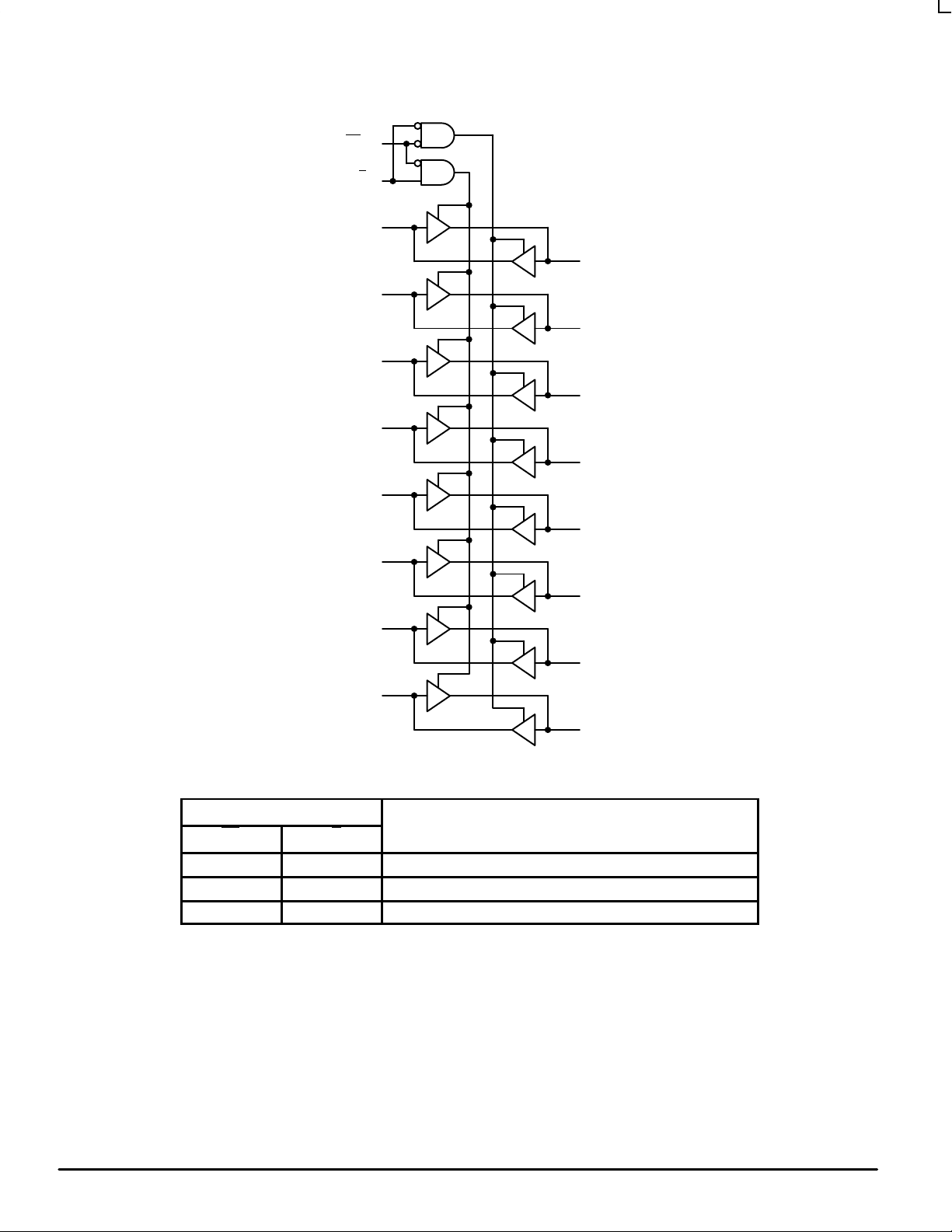
OPERATING MODE
OE
T/R 2
22
A0
A1
A2
A3
A4
A5
A6
A7
10
3
21
B0
4
20
B1
5
19
B2
6
18
B3
7
17
B4
8
16
B5
9
15
B6
14
B7
Figure 2. Logic Diagram
INPUTS
OE T/R
L L B Data to A Bus
L H A Data to B Bus
H X Z
H = High Voltage Level; L = Low V oltage Level; Z = High Impedance State; X = High or Low Voltage Level
and Transitions are Acceptable; For ICC reasons, Do Not Float Inputs
MOTOROLA LVX Data — Low–Voltage CMOS Logic
2
Non–Inverting
BR1492 — Rev 0
Page 3
MC74LVXC3245
ABSOLUTE MAXIMUM RATINGS*
Symbol Parameter Value Condition Unit
V
, V
CCA
CCB
V
I
V
I/O
I
IK
I
OK
I
O
ICC, I
GND
T
STG
* Absolute maximum continuous ratings are those values beyond which damage to the device may occur. Exposure to these conditions or conditions
beyond those indicated may adversely affect device reliability. Functional operation under absolute–maximum–rated conditions is not implied.
RECOMMENDED OPERATING CONDITIONS
Symbol Parameter Min Max Unit
V
, V
CCA
CCB
V
I
V
I/O
T
A
∆t/∆V Minimum Input Edge Rate
DC Supply Voltage –0.5 to +7.0 V
DC Input Voltage OE, T/R –0.5 to V
DC Input/Output Voltage An –0.5 to V
Bn –0.5 to V
DC Input Diode Current OE, T/R ±20 VI < GND mA
DC Output Diode Current ±50 VO < GND; VO > V
DC Output Source/Sink Current ±50 mA
DC Supply Current Per Output Pin
Storage Temperature Range –65 to +150 °C
DC Latchup Source/Sink Current ±300 mA
Supply Voltage (V
Input Voltage OE, T/R 0 V
Input/Output Voltage An
Operating Free–Air Temperature –40 +85 °C
VIN from 30% to 70% of VCC; VCC at 3.0V , 4.5V, 5.5V
CCA
≤ V
CCB
Maximum Current
)V
V
CCA
CCB
Bn
+0.5 V
CCA
+0.5 V
CCA
+0.5 V
CCB
±50
±200
2.7
3.0
0
0
0 8 ns/V
V
V
3.6
5.5
CCA
CCA
CCB
CC
mA
mA
V
V
V
DC ELECTRICAL CHARACTERISTICS
Symbol Parameter Condition V
V
V
V
V
V
V
IHA
IHB
ILA
ILB
OHA
OHB
Minimum HIGH Level
Input Voltage
Maximum LOW Level
Input Voltage
Minimum HIGH Level
Output Voltage
An
OE
T/R
Bn
An
OE
T/R
Bn
V
≤ 0.1V
OUT
or
≥ VCC – 0.1V
V
≤ 0.1V
OUT
or
≥ VCC – 0.1V
I
= –100µA
OUT
IOH = –12mA
IOH = –24mA
IOH = –12mA
IOH = –24mA
I
= –100µA
OUT
IOH = –12mA
IOH = –24mA
IOH = –24mA
CCAVCCB
2.7
3.0
3.6
2.7
3.0
3.6
2.7
3.0
3.6
2.7
3.0
3.6
3.0
3.0
3.0
2.7
2.7
3.0
3.0
3.0
3.0
3.0
3.6
5.5
3.0
3.6
5.5
3.0
3.6
5.5
3.0
3.6
5.5
3.0
3.0
3.0
3.0
4.5
3.0
3.0
3.0
4.5
TA = 25°C TA = –40 to +85°C
Typ Guaranteed Limits Unit
2.99
2.85
2.65
2.50
2.30
2.99
2.85
2.65
4.25
2.0
2.0
2.0
2.00
2.00
3.85
0.8
0.8
0.8
0.80
0.80
1.65
2.90
2.56
2.35
2.30
2.10
2.90
2.56
2.35
3.86
2.0
2.0
2.0
2.00
2.00
3.85
0.8
0.8
0.8
0.80
0.80
1.65
2.90
2.46
2.25
2.20
2.00
2.90
2.46
2.25
3.76
V
V
V
V
V
V
LVX Data — Low–Voltage CMOS Logic
BR1492 — Rev 0
3 MOTOROLA
Page 4

MC74LVXC3245
DC ELECTRICAL CHARACTERISTICS
TA = –40 to +85°CTA = 25°C
Symbol UnitGuaranteed LimitsTypV
V
OLA
V
OLB
I
IN
I
OZA
I
OZB
∆I
CC
I
CCA1
I
CCA2
I
CCB
V
OLPA
V
OLPB
V
OLVA
V
OLVB
V
IHDA
V
IHDB
V
ILDA
V
ILDB
1. Worst case package.
2. Max number of outputs defined as (n). Data inputs are driven 0V to VCC level; one output at GND.
3. Max number of data inputs (n) switching. (n–1) inputs switching 0V to VCC level. Input under test switching: VCC level to threshold (V
to threshold (V
Maximum LOW Level
Output Voltage
Max Input Leakage
Current
Max 3–State Output
Leakage
Max 3–State Output
Leakage
Maximum ICC/Input Bn VI=V
Quiescent V
Current as B Port
Floats
Quiescent V
Current
Quiescent V
Current
Quiet Output Max
Dynamic V
Quiet Output Min
Dynamic V
Min HIGH Level
Dynamic Input Voltage
Max LOW Level
Dynamic Input Voltage
ILD
Supply
CCA
Supply
CCA
Supply
CCB
OL
OL
), f = 1MHz.
OE,
T/R
An
Bn
All
Inputs
ConditionParameter
I
= 100µA
OUT
IOL = 24mA
IOL = 12mA
IOL = 24mA
I
= 100µA
OUT
IOL = 24mA
IOL = 24mA
VI = V
VI = VIH, V
VO = V
VI = VIH, V
VO = V
VI=VCC–0.6V 3.6 3.6 0.35 0.5
An=V
V
An=V
Bn=V
An=V
Bn=V
Notes NO TAG,
Notes NO TAG,
Notes NO TAG,
Notes NO TAG,
Notes NO TAG,
Notes NO TAG,
Notes NO TAG,
Notes NO TAG,
, GND
CCA
= V
OE
CCA
, GND
CCA
= V
OE
CCA
, GND
CCB
–2.1V 3.6 5.5 1.0 1.35 1.5 mA
CCB
or GND
CCA
Bn=Open,
=V
OE
CCA
=V
T/R
CCA
=Open
CCB
or GND
CCA
or GND,
CCB
=GND,
OE
=GND
T/R
or GND
CCA
or GND,
CCB
=GND,
OE
=V
T/R
CCA
NO TAG
NO TAG
NO TAG
NO TAG
NO TAG
NO TAG
NO TAG
NO TAG
V
CCA
3.0
3.0
2.7
2.7
3.0
3.0
3.0
3.6
3.6
IL
IL
,
,
3.6
3.6
3.6
3.6
3.6 Open 5 50
3.6
3.6
3.6
3.6
3.3
3.3
3.3
3.3
3.3
3.3
3.3
3.3
3.3
3.3
3.3
3.3
3.3
3.3
3.3
3.3
CCB
3.0
3.0
3.0
4.5
3.0
3.0
4.5
3.6
5.5
3.6
5.5
3.6
5.5
3.6
5.5
3.6
5.5
3.3
5.0
3.3
5.0
3.3
5.0
3.3
5.0
3.3
5.0
3.3
5.0
3.3
5.0
3.3
5.0
0.002
0.21
0.11
0.22
0.002
0.21
0.18
0.10
0.36
0.36
0.42
0.10
0.36
0.36
±0.1
±0.1
±0.5
±0.5
±0.5
±0.5
5
5
5
8
0.8
0.8
0.8
1.5
–0.8
–0.8
–0.8
–1.2
2.0
2.0
2.0
3.5
0.8
0.8
0.8
1.5
0.10
0.44
0.44
0.50
0.10
0.44
0.44
±1.0
±1.0
±5.0
±5.0
±5.0
±5.0
50
50
50
80
IHD
V
V
µA
µA
µA
mA
µA
µA
µA
V
V
V
V
V
V
V
V
), 0V
MOTOROLA LVX Data — Low–Voltage CMOS Logic
4
BR1492 — Rev 0
Page 5

MC74LVXC3245
AC ELECTRICAL CHARACTERISTICS
TA = –40 to +85°C; CL = 50pF
V
= 2.7–3.6V
CCA
V
= 4.5–5.5V
CCB
Symbol Parameter Min
t
PHL
t
PLH
t
PHL
t
PLH
t
PZL
t
PZH
t
PZL
t
PZH
t
PHZ
t
PLZ
t
PHZ
t
PLZ
t
OSHL
t
OSLH
4. Typical values at V
5. Typical values at V
6. Skew is defined as the absolute value of the difference between the actual propagation delay for any two separate outputs of the same device.
The specification applies to any outputs switching in the same direction, either HIGH–to–LOW (t
guaranteed by design.
Propagation Delay A to B 1.0
Propagation Delay B to A 1.0
Output Enable Time OE to B 1.0
Output Enable Time OE to A 1.0
Output Disable Time OE to B 1.0
Output Disable Time OE to A 1.0
Output to Output Skew, Data to Output
(Note NO TAG)
CCA
CCA
= 3.3V, V
= 3.3V, V
= 5.0V at 25°C.
CCB
= 3.3V at 25°C.
CCB
1.0
1.0
1.0
1.0
1.0
1.0
Typ
(Note 4.)
4.8
3.9
3.8
4.3
4.7
4.8
5.9
5.4
4.0
3.8
4.6
3.1
1.0 1.5 1.0 1.5
Max Min
8.5
7.0
7.0
8.0
8.5
9.0
10.0
9.5
8.5
8.0
10.0
7.0
V
CCA
V
CCB
(Note 5.)
1.0
1.0
1.0
1.0
1.0
1.0
1.0
1.0
1.0
1.0
1.0
1.0
) or LOW–to–HIGH (t
OSHL
= 2.7–3.6V
= 3.0–3.6V
Typ
5.5
5.2
4.4
5.1
6.0
6.1
6.4
5.8
6.3
4.5
5.2
3.4
Max Unit
9.0
8.5
7.5
8.0
9.5
10.0
10.5
9.5
10.0
8.5
10.0
7.0
OSLH
ns
ns
ns
ns
ns
ns
ns
); parameter
CAPACITIVE CHARACTERISTICS
Symbol Parameter Condition Typical Unit
C
IN
C
I/O
C
PD
Input Capacitance V
Input/Output Capacitance V
Power Dissipation Capacitance A→B
(Measured at 10MHz) B→A
CCA
CCA
= 3.3V; V
= 3.3V; V
V
= 5.0V
CCB
V
= 3.3V
CCA
= 5.0V 4.5 pF
CCB
= 5.0V 10 pF
CCB
50
40
pF
LVX Data — Low–Voltage CMOS Logic
BR1492 — Rev 0
5 MOTOROLA
Page 6

MC74LVXC3245
ISA BUS (IEEE P996)
SD(0:15)
PCMCIA 2.0
JEIDA 4.1
COMPATIBLE
CONTROLLER
SD(0:15)
POWER
SWITCHES
SLOT 0
SLOT 1
5V
V
CC
V
CCA
LVXC3245
LVXC3245
3V
V
CC
LVXC3245
V
CCB
SLOT 0
SLOT 1
Figure 3. Block Diagram
Configurable I/O Application for PCMCIA Cards
The 74LVXC3245 is a dual–supply device well suited for
PCMCIA configurable I/O applications. The LVXC3245
consumes less than 1mW of quiescent power in all modes of
operation, making it ideal for low power notebook designs.
The LVXC3245 meets all PCMCIA I/O voltage requirements
at 5V and 3.3V operation. By tying the V
pin to the card
CCB
LVXC3245
OPTIONAL
voltage supply , the PCMCIA card will always have rail–to–rail
output swings, maximizing the reliability of the interface.
The V
pin must always be tied to a 3.3V power supply .
CCA
This voltage connection provides internal references needed
to account for variations in V
. When connected as in the
CCB
figure above, the LVXC3245 meets all the voltage and
current requirements of the ISA bus standard (IEEE P996).
MOTOROLA LVX Data — Low–Voltage CMOS Logic
6
BR1492 — Rev 0
Page 7

An, Bn
Bn, An
OE, T/R
An, Bn
50% V
CC
t
PLH
50% V
CC
WAVEFORM 1 – PROPAGATION DELAYS
tR = tF = 2.5ns, 10% to 90%; f = 1MHz; tW = 500ns
50% V
CC
t
PZH
50% V
CC
t
PHZ
50% V
50% V
CC
t
PHL
50% V
CC
CC
V
CC
0V
V
OH
V
OL
V
CC
0V
V
CC
VOH – 0.3V
≈
0V
MC74LVXC3245
PULSE
GENERATOR
An, Bn
t
PZL
50% V
WAVEFORM 2 – OUTPUT ENABLE AND DISABLE TIMES
tR = tF = 2.5ns, 10% to 90%; f = 1MHz; tW = 500ns
CC
t
PLZ
Figure 4. AC Waveforms
V
CC
DUT
R
T
TEST SWITCH
t
, t
, t
PLH
PHL
t
, t
PZL
PLZ
CL = 50pF or equivalent (Includes jig and probe capacitance)
RL = R1 = 500Ω or equivalent
RT = Z
OUT
, t
PZH
PHZ
of pulse generator (typically 50Ω)
≈
V
CC
VOL + 0.3V
GND
2xV
CC
R
1
C
R
L
Open
2xV
L
CC
OPEN
LVX Data — Low–Voltage CMOS Logic
BR1492 — Rev 0
Figure 5. T est Circuit
7 MOTOROLA
Page 8

MC74LVXC3245
U0.15 (0.006) T
U0.15 (0.006) T
–T–
S
L
S
0.10 (0.004)
SEATING
PLANE
2X L/2
PIN 1
IDENT.
D
OUTLINE DIMENSIONS
DT SUFFIX
PLASTIC TSSOP PACKAGE
CASE 948H–01
ISSUE O
24X REFK
0.10 (0.004) V
24
1
M
A
–V–
C
G
S
U
T
S
NOTES:
1 DIMENSIONING AND TOLERANCING PER ANSI
13
B
–U–
12
H
–W–
Y14.5M, 1982.
2 CONTROLLING DIMENSION: MILLIMETER.
3 DIMENSION A DOES NOT INCLUDE MOLD FLASH,
PROTRUSIONS OR GATE BURRS. MOLD FLASH
OR GATE BURRS SHALL NOT EXCEED 0.15
(0.006) PER SIDE.
4 DIMENSION B DOES NOT INCLUDE INTERLEAD
FLASH OR PROTRUSION. INTERLEAD FLASH OR
PROTRUSION SHALL NOT EXCEED
0.25 (0.010) PER SIDE.
5 DIMENSION K DOES NOT INCLUDE DAMBAR
PROTRUSION. ALLOWABLE DAMBAR
PROTRUSION SHALL BE 0.08 (0.003) TOTAL IN
EXCESS OF THE K DIMENSION AT MAXIMUM
MATERIAL CONDITION.
6 TERMINAL NUMBERS ARE SHOWN FOR
REFERENCE ONLY.
7 DIMENSION A AND B ARE TO BE DETERMINED
AT DATUM PLANE –W–.
DIM MIN MAX MIN MAX
A 7.70 7.90 0.303 0.311
B 4.30 4.50 0.169 0.177
C ––– 1.20 ––– 0.047
D 0.05 0.15 0.002 0.006
F 0.50 0.75 0.020 0.030
G 0.65 BSC 0.026 BSC
H 0.27 0.37 0.011 0.015
J 0.09 0.20 0.004 0.008
J1 0.09 0.16 0.004 0.006
K 0.19 0.30 0.007 0.012
K1 0.19 0.25 0.007 0.010
L 6.40 BSC 0.252 BSC
M 0 8 0 8
____
INCHESMILLIMETERS
DETAIL E
K
N
K1
J1
SECTION N–N
J
N
F
DETAIL E
0.25 (0.010)
M
MOTOROLA LVX Data — Low–Voltage CMOS Logic
8
BR1492 — Rev 0
Page 9

OUTLINE DIMENSIONS
PLASTIC SOIC PACKAGE
CASE 751E–04
–A
–
24 13
–B
P 12 PL
–
112
D 24 PL
0.010 (0.25) A B
M
S S
T
C
–T
–
SEATING
PLANE
G 22 PL
K
0.010 (0.25)
DW SUFFIX
ISSUE E
M M
J
F
M
B
R X 45°
MC74LVXC3245
NOTES:
1. DIMENSIONING AND TOLERANCING PER
ANSI Y14.5M, 1982.
2. CONTROLLING DIMENSION: MILLIMETER.
3. DIMENSIONS A AND B DO NOT INCLUDE
MOLD PROTRUSION.
4. MAXIMUM MOLD PROTRUSION 0.15
(0.006) PER SIDE.
5. DIMENSION D DOES NOT INCLUDE
DAMBAR PROTRUSION. ALLOWABLE
DAMBAR PROTRUSION SHALL BE 0.13
(0.005) TOTAL IN EXCESS OF D
DIMENSION AT MAXIMUM MATERIAL
CONDITION.
MILLIMETERS INCHES
MIN MINMAX MAX
DIM
A
B
C
D
F
G
J
K
M
P
R
15.54
7.60
2.65
0.49
0.90
0.32
0.29
8
10.55
0.75
0.601
0.292
0.093
0.014
0.016
0.009
0.005
0
°
°
0.395
0.010
15.25
7.40
2.35
0.35
0.41
1.27 BSC 0.050 BSC
0.23
0.13
0
°
10.05
0.25
0.612
0.299
0.104
0.019
0.035
0.013
0.011
8
°
0.415
0.029
Motorola reserves the right to make changes without further notice to any products herein. Motorola makes no warranty , representation or guarantee regarding
the suitability of its products for any particular purpose, nor does Motorola assume any liability arising out of the application or use of any product or circuit, and
specifically disclaims any and all liability, including without limitation consequential or incidental damages. “T ypical” parameters which may be provided in Motorola
data sheets and/or specifications can and do vary in different applications and actual performance may vary over time. All operating parameters, including “Typicals”
must be validated for each customer application by customer’s technical experts. Motorola does not convey any license under its patent rights nor the rights of
others. Motorola products are not designed, intended, or authorized for use as components in systems intended for surgical implant into the body, or other
applications intended to support or sustain life, or for any other application in which the failure of the Motorola product could create a situation where personal injury
or death may occur. Should Buyer purchase or use Motorola products for any such unintended or unauthorized application, Buyer shall indemnify and hold Motorola
and its officers, employees, subsidiaries, affiliates, and distributors harmless against all claims, costs, damages, and expenses, and reasonable attorney fees
arising out of, directly or indirectly, any claim of personal injury or death associated with such unintended or unauthorized use, even if such claim alleges that
Motorola was negligent regarding the design or manufacture of the part. Motorola and are registered trademarks of Motorola, Inc. Motorola, Inc. is an Equal
Opportunity/Affirmative Action Employer.
Mfax is a trademark of Motorola, Inc.
How to reach us:
USA/EUROPE/Locations Not Listed: Motorola Literature Distribution; JAPAN: Nippon Motorola Ltd.: SPD, Strategic Planning Office, 4–32–1,
P.O. Box 5405, Denver, Colorado 80217. 303–675–2140 or 1–800–441–2447 Nishi–Gotanda, Shinagawa–ku, Tokyo 141, Japan. 81–3–5487–8488
Mfax: RMFAX0@email.sps.mot.com – TOUCHT ONE 602–244–6609 ASIA/PACIFIC: Motorola Semiconductors H.K. Ltd.; 8B Tai Ping Industrial Park,
– US & Canada ONLY 1–800–774–1848 51 Ting Kok Road, Tai Po, N.T., Hong Kong. 852–26629298
INTERNET: http://motorola.com/sps
LVX Data — Low–Voltage CMOS Logic
◊
9 MOTOROLA
MC74LVXC3245/D
BR1492 — Rev 0
 Loading...