

Page 1
SEMICONDUCTOR TECHNICAL DATA
1
REV 0
Motorola, Inc. 1997
6/97
"
!
The MC74LVX373 is an advanced high speed CMOS octal latch with
3–state outputs. The inputs tolerate voltages up to 7V, allowing the
interface of 5V systems to 3V systems.
This 8–bit D–type latch is controlled by a latch enable input and an
output enable input. When the output enable input is high, the eight
outputs are in a high impedance state.
• High Speed: t
PD
= 5.8ns (Typ) at VCC = 3.3V
• Low Power Dissipation: I
CC
= 4µA (Max) at TA = 25°C
• Power Down Protection Provided on Inputs
• Balanced Propagation Delays
• Low Noise: V
OLP
= 0.8V (Max)
• Pin and Function Compatible with Other Standard Logic Families
• Latchup Performance Exceeds 300mA
• ESD Performance: HBM > 2000V; Machine Model > 200V
Figure 1. 20–Lead Pinout (Top View)
1920 18 17 16 15 14
21 34567
V
CC
13
8
12
9
11
10
O7 D7 D6 O6 O5 D5 D4 O4 LE
OE
O0 D0 D1 O1 O2 D2 D3 O3 GND
LVX
LOW–VOLTAGE CMOS
DW SUFFIX
20–LEAD SOIC PACKAGE
CASE 751D–04
DT SUFFIX
20–LEAD TSSOP PACKAGE
CASE 948E–02
M SUFFIX
20–LEAD SOIC EIAJ PACKAGE
CASE 967–01
PIN NAMES
Function
Output Enable Input
Latch Enable Input
Data Inputs
3–State Latch Outputs
Pins
OE
LE
D0–D7
O0–O7
Page 2
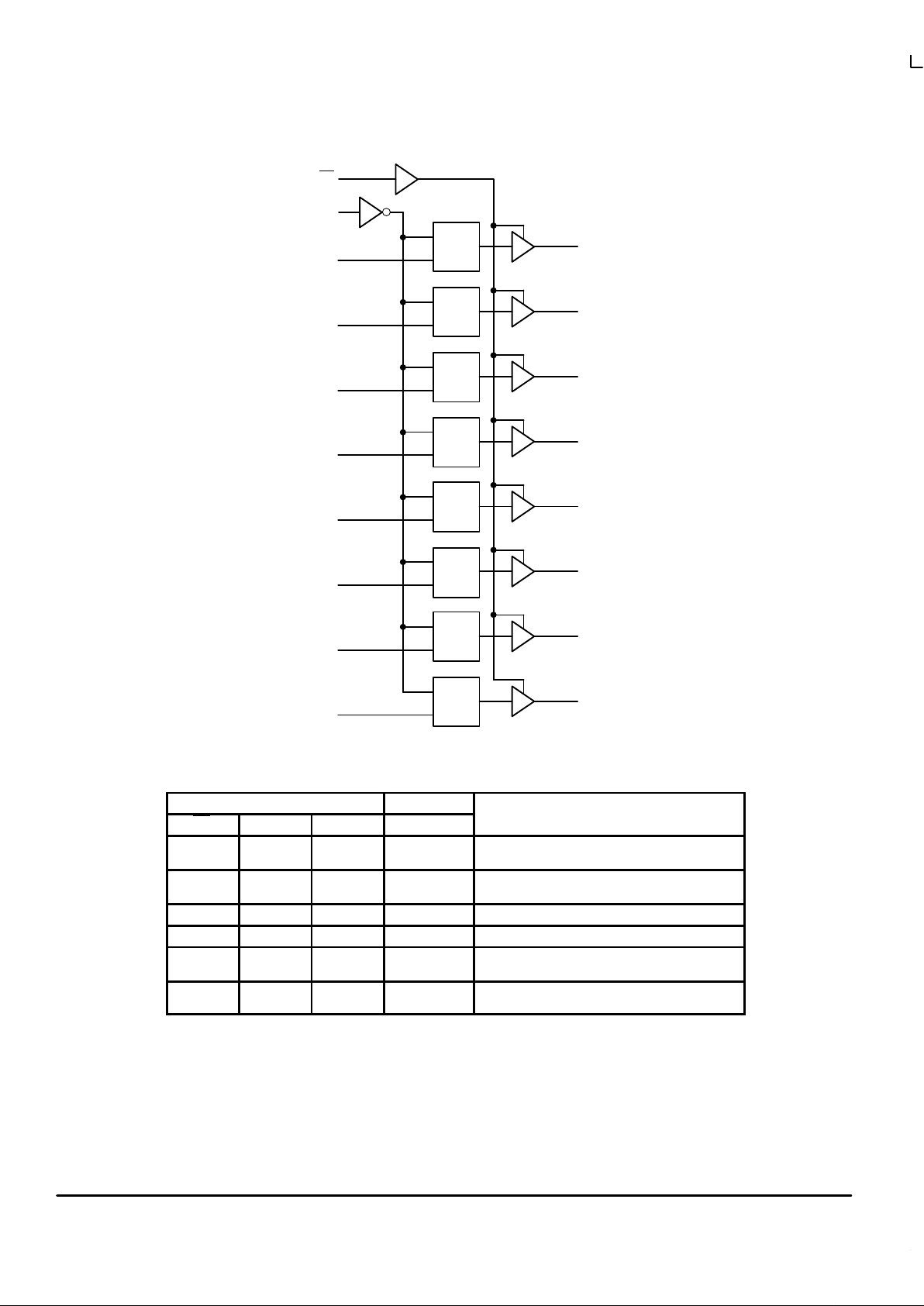
MC74LVX373
MOTOROLA LCX DATA
BR1339 — REV 3
2
O0
D0
O1
D1
O2
D2
O3
D3
O4
D4
O5
D5
O6
D6
O7
D7
Figure 2. Logic Diagram
nLE
Q
D
nLE
Q
D
nLE
Q
D
nLE
Q
D
nLE
Q
D
nLE
Q
D
nLE
Q
D
nLE
Q
D
LE
OE
3
4
7
8
13
14
17
18
2
5
6
9
12
15
16
19
11
1
INPUTS OUTPUTS
OE LE Dn On OPERATING MODE
L
L
H
H
H
L
H
L
Transparent (Latch Disabled); Read Latch
L
L
L
L
h
l
H
L
Latched (Latch Enabled) Read Latch
L L X NC Hold; Read Latch
H L X Z Hold; Disabled Outputs
H
H
H
H
H
L
Z
Z
Transparent (Latch Disabled); Disabled Outputs
H
H
L
L
h
l
Z
Z
Latched (Latch Enabled); Disabled Outputs
H = High Voltage Level; h = High Voltage Level One Setup Time Prior to the Latch Enable High–to–Low
Transition; L = Low V oltage Level; l = Low Voltage Level One Setup Time Prior to the Latch Enable High–to–Low
Transition; NC = No Change, State Prior to the Latch Enable High–to–Low T ransition; X = High or Low V oltage
Level or Transitions are Acceptable; Z = High Impedance State; For ICC Reasons DO NOT FLOAT Inputs
Page 3
MC74LVX373
LCX DATA
BR1339 — REV 3
3 MOTOROLA
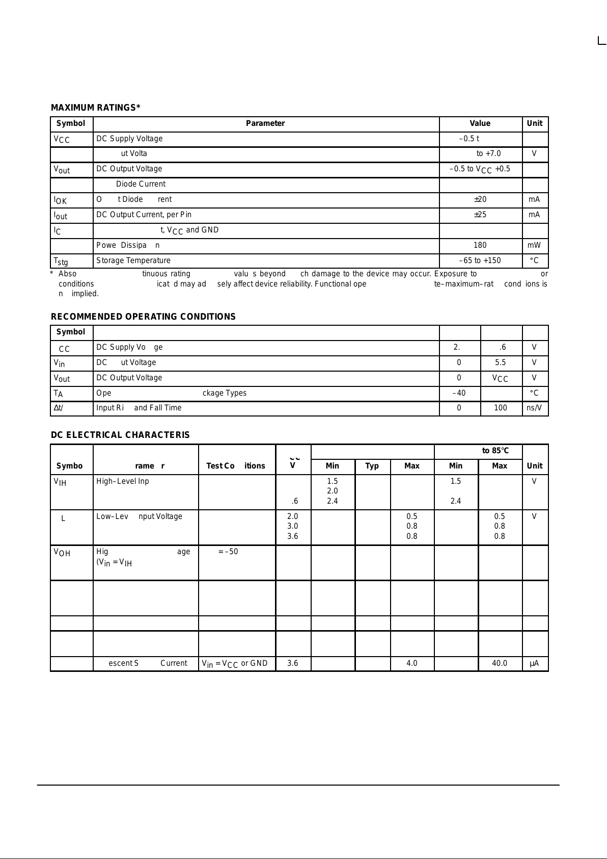
MAXIMUM RATINGS*
Symbol
Parameter
Value
Unit
V
CC
DC Supply Voltage
–0.5 to +7.0
V
V
in
DC Input Voltage
–0.5 to +7.0
V
V
out
DC Output Voltage
–0.5 to VCC +0.5
V
I
IK
Input Diode Current
–20
mA
I
OK
Output Diode Current
±20
mA
I
out
DC Output Current, per Pin
±25
mA
I
CC
DC Supply Current, VCC and GND Pins
±75
mA
P
D
Power Dissipation
180
mW
T
stg
Storage Temperature
–65 to +150
_
C
* Absolute maximum continuous ratings are those values beyond which damage to the device may occur. Exposure to these conditions or
conditions beyond those indicated may adversely affect device reliability. Functional operation under absolute–maximum–rated conditions is
not implied.
RECOMMENDED OPERATING CONDITIONS
Symbol
Parameter
Min
Max
Unit
V
CC
DC Supply Voltage
2.0
3.6
V
V
in
DC Input Voltage
0
5.5
V
V
out
DC Output Voltage
0
V
CC
V
T
A
Operating Temperature, All Package Types
–40
+85
_
C
∆t/∆V
Input Rise and Fall Time
0
100
ns/V
DC ELECTRICAL CHARACTERISTICS
ОООООО
V
TA = 25°C
TA = – 40 to 85°C
Symbol
Parameter
ОООООО
Test Conditions
V
CC
V
Min
Typ
Max
Min
Max
Unit
ÎÎ
Î
V
IH
ОООООО
Î
High–Level Input Voltage
ОООООО
ОООООÎÎ
Î
2.0
3.0
3.6
ÎÎ
Î
1.5
2.0
2.4
ÎÎÎÎÎÎÎ
Î
1.5
2.0
2.4
ÎÎÎÎ
V
ÎÎ
Î
V
IL
ОООООО
Î
Low–Level Input Voltage
ОООООО
ОООООÎÎ
Î
2.0
3.0
3.6
ÎÎÎÎÎÎÎ
Î
0.5
0.8
0.8
ÎÎÎÎÎ
Î
0.5
0.8
0.8
Î
V
ÎÎ
Î
ÎÎ
Î
V
OH
ОООООО
Î
ОООООО
Î
High–Level Output Voltage
(Vin = VIH or VIL)
ОООООО
ООООО
Î
ООООО
Î
IOH = –50µA
IOH = –50µA
IOH = –4mA
Î
Î
Î
Î
2.0
3.0
3.0
ÎÎ
Î
ÎÎ
Î
1.9
2.9
2.58
Î
Î
Î
Î
2.0
3.0
ÎÎ
Î
ÎÎ
Î
ÎÎ
Î
ÎÎ
Î
1.9
2.9
2.48
ÎÎ
Î
ÎÎ
Î
Î
Î
V
ÎÎ
Î
V
OL
ОООООО
Î
Low–Level Output Voltage
(Vin = VIH or VIL)
ОООООО
ООООО
Î
IOL = 50µA
IOL = 50µA
IOL = 4mA
Î
Î
2.0
3.0
3.0
ÎÎÎÎ
Î
0.0
0.0
ÎÎ
Î
0.1
0.1
0.36
ÎÎÎÎÎ
Î
0.1
0.1
0.44
Î
V
I
in
Input Leakage Current
ОООООО
Vin = 5.5V or GND
3.6
±0.1
±1.0
µA
ÎÎ
Î
I
OZ
ОООООО
Î
Maximum Three–State
Leakage Current
ОООООО
ООООО
Î
Vin = VIL or V
IH
V
out
= VCC or GND
Î
Î
3.6
ÎÎÎÎÎÎÎ
Î
±0.25
ÎÎÎÎÎ
Î
±2.5
Î
µA
I
CC
Quiescent Supply Current
ОООООО
Vin = VCC or GND
3.6
4.0
40.0
µA
Page 4

MC74LVX373
MOTOROLA LCX DATA
BR1339 — REV 3
4
AC ELECTRICAL CHARACTERISTICS (Input t
r
= tf = 3.0ns)
TA = 25°C
TA = – 40 to 85°C
Symbol
Parameter
Test Conditions
Min
Typ
Max
Min
Max
Unit
ÎÎ
Î
t
PLH
,
t
PHL
ОООООО
Î
Propagation Delay
D to O
ООООООО
Î
VCC = 2.7V CL = 15pF
CL = 50pF
ÎÎÎÎ
Î
7.5
10.0
ÎÎ
Î
14.5
18.0
Î
Î
1.0
1.0
ÎÎ
Î
17.5
21.0
ns
ÎÎÎООООООÎООООООО
Î
VCC = 3.3 ± 0.3V CL = 15pF
CL = 50pF
ÎÎÎÎ
Î
5.8
8.3
ÎÎ
Î
9.3
12.8
Î
Î
1.0
1.0
ÎÎ
Î
11.0
14.5
ÎÎ
Î
t
PLH
,
t
PHL
ОООООО
Î
Propagation Delay
LE to O
ООООООО
Î
VCC = 2.7V CL = 15pF
CL = 50pF
ÎÎÎÎ
Î
7.7
10.2
ÎÎ
Î
15.0
18.5
Î
Î
1.0
1.0
ÎÎ
Î
18.5
22.0
ns
ÎÎÎООООООÎООООООО
Î
VCC = 3.3 ± 0.3V CL = 15pF
CL = 50pF
ÎÎÎÎ
Î
6.0
8.5
ÎÎ
Î
9.7
13.2
Î
Î
1.0
1.0
ÎÎ
Î
11.5
15.0
ÎÎ
Î
t
PZL
,
t
PZH
ОООООО
Î
Output Enable Time
OE
to O
ООООООО
Î
VCC = 2.7V CL = 15pF
RL = 1kΩ CL = 50pF
ÎÎÎÎ
Î
7.7
10.2
ÎÎ
Î
15.0
18.5
Î
Î
1.0
1.0
ÎÎ
Î
18.5
22.0
ns
VCC = 3.3 ± 0.3V CL = 15pF
RL = 1kΩ CL = 50pF
6.0
8.5
9.7
13.2
1.0
1.0
11.5
15.0
ÎÎ
Î
t
PLZ
,
t
PHZ
ОООООО
Î
Output Disable Time
OE
to O
ООООООО
Î
VCC = 2.7V CL = 50pF
RL = 1kΩ
ÎÎÎÎ
Î
9.8
ÎÎ
Î
18.0
Î
Î
1.0
ÎÎ
Î
21.0
ns
ÎÎÎООООООÎООООООО
Î
VCC = 3.3 ± 0.3V CL = 50pF
RL = 1kΩ
ÎÎÎÎ
Î
8.2
ÎÎ
Î
12.8
Î
Î
1.0
ÎÎ
Î
14.5
t
OSHL
t
OSLH
Output–to–Output Skew
(Note 1.)
VCC = 2.7V CL = 50pF
VCC = 3.3 ±0.3V CL = 50pF
1.5
1.5
1.5
1.5
ns
1. Skew is defined as the absolute value of the difference between the actual propagation delay for any two separate outputs of the same device.
The specification applies to any outputs switching in the same direction, either HIGH–to–LOW (t
OSHL
) or LOW–to–HIGH (t
OSLH
); parameter
guaranteed by design.
CAPACITIVE CHARACTERISTICS
TA = 25°C
TA = – 40 to 85°C
Symbol
Parameter
Min
Typ
Max
Min
Max
Unit
C
in
Input Capacitance
4
10
10
pF
C
out
Maximum Three–State Output Capacitance
6
pF
C
PD
Power Dissipation Capacitance (Note 2.)
27
pF
2. CPD is defined as the value of the internal equivalent capacitance which is calculated from the operating current consumption without load.
Average operating current can be obtained by the equation: I
CC(OPR
)
= CPD VCC fin + ICC/8 (per latch). CPD is used to determine the no–load
dynamic power consumption; PD = CPD V
CC
2
fin + ICC VCC.
NOISE CHARACTERISTICS (Input t
r
= tf = 3.0ns, CL = 50pF, VCC = 3.3V , Measured in SOIC Package)
TA = 25°C
Symbol Characteristic
Typ Max
Unit
V
OLP
Quiet Output Maximum Dynamic V
OL
0.5 0.8 V
V
OLV
Quiet Output Minimum Dynamic V
OL
–0.5 –0.8 V
V
IHD
Minimum High Level Dynamic Input Voltage 2.0 V
V
ILD
Maximum Low Level Dynamic Input Voltage 0.8 V
Page 5

MC74LVX373
LCX DATA
BR1339 — REV 3
5 MOTOROLA
TIMING REQUIREMENTS (Input t
r
= tf = 3.0ns)
TA = 25°C
TA = – 40
to 85°C
Symbol Parameter Test Conditions
Typ Limit Limit
Unit
t
w(h)
Minimum Pulse Width, LE VCC = 2.7V
VCC = 3.3 ±0.3V
6.5
5.0
7.5
5.0
ns
t
su
Minimum Setup Time, D to LE VCC = 2.7V
VCC = 3.3 ±0.3V
6.0
4.0
6.0
4.0
ns
t
h
Minimum Hold Time, D to LE VCC = 2.7V
VCC = 3.3 ±0.3V
1.0
1.0
1.0
1.0
ns
V
CC
GND
D
O
50%
50% VCC
t
PLH
t
PHL
V
CC
GND
50%
LE
t
PLH
t
PHL
O
t
w
50% VCC
Figure 3. Figure 4.
50%
50% VCC
50% VCC
O
t
PZL
t
PLZ
t
PZHtPHZ
VOL +0.3V
VOL –0.3V
V
CC
GND
HIGH
IMPEDANCE
HIGH
IMPEDANCE
O
OE
50%
D
LE
V
CC
V
CC
GND
GND
VALID
t
h
t
su
50%
Figure 5. Figure 6.
SWITCHING W AVEFORMS
*Includes all probe and jig capacitance
CL*
TEST POINT
DEVICE
UNDER
TEST
OUTPUT
*Includes all probe and jig capacitance
CL*
TEST POINT
DEVICE
UNDER
TEST
OUTPUT
CONNECT TO VCC WHEN
TESTING t
PLZ
AND t
PZL
.
CONNECT TO GND WHEN
TESTING t
PHZ
AND t
PZH
.
1 k
Ω
TEST CIRCUITS
Figure 7. Propagation Delay Test Circuit Figure 8. Three–State Test Circuit
Page 6

MC74LVX373
MOTOROLA LCX DATA
BR1339 — REV 3
6
OUTLINE DIMENSIONS
DW SUFFIX
PLASTIC SOIC PACKAGE
CASE 751D–04
ISSUE E
NOTES:
1. DIMENSIONING AND TOLERANCING PER
ANSI Y14.5M, 1982.
2. CONTROLLING DIMENSION: MILLIMETER.
3. DIMENSIONS A AND B DO NOT INCLUDE
MOLD PROTRUSION.
4. MAXIMUM MOLD PROTRUSION 0.150
(0.006) PER SIDE.
5. DIMENSION D DOES NOT INCLUDE
DAMBAR PROTRUSION. ALLOWABLE
DAMBAR PROTRUSION SHALL BE 0.13
(0.005) TOTAL IN EXCESS OF D DIMENSION
AT MAXIMUM MATERIAL CONDITION.
–A–
–B–
20
1
11
10
S
A
M
0.010 (0.25) B
S
T
D20X
M
B
M
0.010 (0.25)
P10X
J
F
G
18X
K
C
–T–
SEATING
PLANE
M
R
X 45
_
DIM MIN MAX MIN MAX
INCHESMILLIMETERS
A 12.65 12.95 0.499 0.510
B 7.40 7.60 0.292 0.299
C 2.35 2.65 0.093 0.104
D 0.35 0.49 0.014 0.019
F 0.50 0.90 0.020 0.035
G 1.27 BSC 0.050 BSC
J 0.25 0.32 0.010 0.012
K 0.10 0.25 0.004 0.009
M 0 7 0 7
P 10.05 10.55 0.395 0.415
R 0.25 0.75 0.010 0.029
__
__
DT SUFFIX
PLASTIC TSSOP PACKAGE
CASE 948E–02
ISSUE A
DIMAMIN MAX MIN MAX
INCHES
6.60 0.260
MILLIMETERS
B 4.30 4.50 0.169 0.177
C 1.20 0.047
D 0.05 0.15 0.002 0.006
F 0.50 0.75 0.020 0.030
G 0.65 BSC 0.026 BSC
H 0.27 0.37 0.011 0.015
J 0.09 0.20 0.004 0.008
J1 0.09 0.16 0.004 0.006
K 0.19 0.30 0.007 0.012
K1 0.19 0.25 0.007 0.010
L 6.40 BSC 0.252 BSC
M 0 8 0 8
____
NOTES:
1. DIMENSIONING AND TOLERANCING PER ANSI
Y14.5M, 1982.
2. CONTROLLING DIMENSION: MILLIMETER.
3. DIMENSION A DOES NOT INCLUDE MOLD FLASH,
PROTRUSIONS OR GATE BURRS. MOLD FLASH
OR GATE BURRS SHALL NOT EXCEED 0.15
(0.006) PER SIDE.
4. DIMENSION B DOES NOT INCLUDE INTERLEAD
FLASH OR PROTRUSION. INTERLEAD FLASH OR
PROTRUSION SHALL NOT EXCEED 0.25 (0.010)
PER SIDE.
5. DIMENSION K DOES NOT INCLUDE DAMBAR
PROTRUSION. ALLOWABLE DAMBAR
PROTRUSION SHALL BE 0.08 (0.003) TOTAL IN
EXCESS OF THE K DIMENSION AT MAXIMUM
MATERIAL CONDITION.
6. TERMINAL NUMBERS ARE SHOWN FOR
REFERENCE ONLY.
7. DIMENSION A AND B ARE TO BE DETERMINED
AT DATUM PLANE –W–.
110
1120
PIN 1
IDENT
A
B
–T–
0.100 (0.004)
C
D
G
H
SECTION N–N
K
K1
JJ1
N
N
M
F
–W–
SEATING
PLANE
–V–
–U–
S
U
M
0.10 (0.004) V
S
T
20X REFK
L
L/2
2X
S
U0.15 (0.006) T
DETAIL E
0.25 (0.010)
DETAIL E
6.40 0.252
––– –––
S
U0.15 (0.006) T
Page 7

MC74LVX373
LCX DATA
BR1339 — REV 3
7 MOTOROLA
OUTLINE DIMENSIONS
M SUFFIX
PLASTIC SOIC EIAJ PACKAGE
CASE 967–01
ISSUE O
DIM MIN MAX MIN MAX
INCHES
––– 2.05 ––– 0.081
MILLIMETERS
0.05 0.20 0.002 0.008
0.35 0.50 0.014 0.020
0.18 0.27 0.007 0.011
12.35 12.80 0.486 0.504
5.10 5.45 0.201 0.215
1.27 BSC 0.050 BSC
7.40 8.20 0.291 0.323
0.50 0.85 0.020 0.033
1.10 1.50 0.043 0.059
0
0.70 0.90 0.028 0.035
––– 0.81 ––– 0.032
A
1
H
E
Q
1
L
E
_
10
_
0
_
10
_
NOTES:
1 DIMENSIONING AND TOLERANCING PER ANSI
Y14.5M, 1982.
2 CONTROLLING DIMENSION: MILLIMETER.
3 DIMENSIONS D AND E DO NOT INCLUDE MOLD
FLASH OR PROTRUSIONS AND ARE MEASURED
AT THE PARTING LINE. MOLD FLASH OR
PROTRUSIONS SHALL NOT EXCEED 0.15 (0.006)
PER SIDE.
4 TERMINAL NUMBERS ARE SHOWN FOR
REFERENCE ONLY.
5 THE LEAD WIDTH DIMENSION (b) DOES NOT
INCLUDE DAMBAR PROTRUSION. ALLOWABLE
DAMBAR PROTRUSION SHALL BE 0.08 (0.003)
TOTAL IN EXCESS OF THE LEAD WIDTH
DIMENSION AT MAXIMUM MA TERIAL CONDITION.
DAMBAR CANNOT BE LOCATED ON THE LOWER
RADIUS OR THE FOOT. MINIMUM SPACE
BETWEEN PROTRUSIONS AND ADJACENT LEAD
TO BE 0.46 ( 0.018).
H
E
A
1
L
E
Q
1
_
c
A
Z
D
E
20
110
11
b
M
0.13 (0.005)
e
0.10 (0.004)
VIEW P
DETAIL P
M
L
A
b
c
D
E
e
L
M
Z
Motorola reserves the right to make changes without further notice to any products herein. Motorola makes no warranty , representation or guarantee regarding
the suitability of its products for any particular purpose, nor does Motorola assume any liability arising out of the application or use of any product or circuit, and
specifically disclaims any and all liability, including without limitation consequential or incidental damages. “T ypical” parameters which may be provided in Motorola
data sheets and/or specifications can and do vary in different applications and actual performance may vary over time. All operating parameters, including “Typicals”
must be validated for each customer application by customer’s technical experts. Motorola does not convey any license under its patent rights nor the rights of
others. Motorola products are not designed, intended, or authorized for use as components in systems intended for surgical implant into the body, or other
applications intended to support or sustain life, or for any other application in which the failure of the Motorola product could create a situation where personal injury
or death may occur. Should Buyer purchase or use Motorola products for any such unintended or unauthorized application, Buyer shall indemnify and hold Motorola
and its officers, employees, subsidiaries, affiliates, and distributors harmless against all claims, costs, damages, and expenses, and reasonable attorney fees
arising out of, directly or indirectly, any claim of personal injury or death associated with such unintended or unauthorized use, even if such claim alleges that
Motorola was negligent regarding the design or manufacture of the part. Motorola and are registered trademarks of Motorola, Inc. Motorola, Inc. is an Equal
Opportunity/Affirmative Action Employer.
MC74LVX373/D
◊
Mfax is a trademark of Motorola, Inc.
How to reach us:
USA/EUROPE/Locations Not Listed: Motorola Literature Distribution; JAPAN: Nippon Motorola Ltd.: SPD, Strategic Planning Office, 4–32–1,
P.O. Box 5405, Denver, Colorado 80217. 303–675–2140 or 1–800–441–2447 Nishi–Gotanda, Shinagawa–ku, Tokyo 141, Japan. 81–3–5487–8488
Mfax: RMFAX0@email.sps.mot.com – TOUCHTONE 602–244–6609 ASIA/PACIFIC: Motorola Semiconductors H.K. Ltd.; 8B Tai Ping Industrial Park,
– US & Canada ONLY 1–800–774–1848 51 Ting Kok Road, Tai Po, N.T., Hong Kong. 852–26629298
INTERNET: http://motorola.com/sps
 Loading...