

Page 1
SEMICONDUCTOR TECHNICAL DATA
The MC74LVQ74 is a high performance, dual D–type flip–flop with
asynchronous clear and set inputs and complementary (O, O
operates from a 2.7 to 3.6V supply. High impedance TTL compatible
inputs significantly reduce current loading to input drivers while TTL
compatible outputs offer improved switching noise performance.
The MC74L VQ74 consists of 2 edge–triggered flip–flops with individual
D–type inputs. The flip–flop will store the state of individual D inputs, that
meet the setup and hold time requirements, on the LOW–to–HIGH Clock
(CP) transition.
) outputs. It
LVQ
LOW–VOLTAGE CMOS
DUAL D–TYPE FLIP–FLOP
• Designed for 2.7 to 3.6V V
Noise Applications
Operation – Ideal for Low Power/Low
CC
• Guaranteed Simultaneous Switching Noise Level and Dynamic
Threshold Performance
• Guaranteed Skew Specifications
• Guaranteed Incident Wave Switching into 75Ω
• Low Static Supply Current (10µA) Substantially Reduces System Power
Requirements
• Latchup Performance Exceeds 500mA
• ESD Performance: Human Body Model >2000V
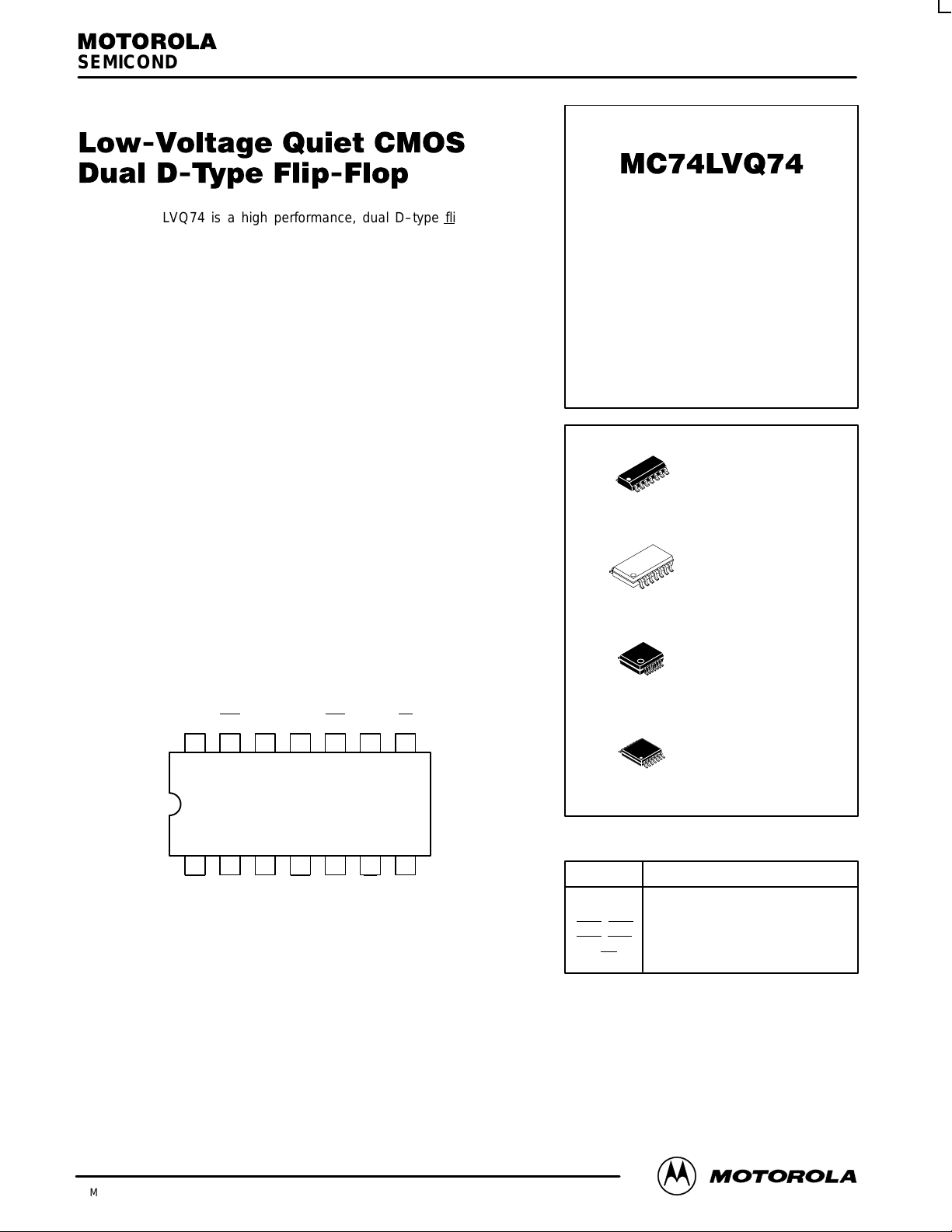
Pinout: 14–Lead (Top View)
VCCCD2
CD1 D1 CP1 SD1 O1 O1 GND
D2 CP2 SD2 O2 O2
1314 12 11 10 9 8
21 34567
14
14
14
14
PIN NAMES
Pins
CP1, CP2
D1, D2
CD1
, CD2
SD1, SD2
On, On
1
1
1
1
Function
Clock Pulse Inputs
Data Inputs
Direct Clear Inputs
Direct Set Inputs
Outputs
D SUFFIX
PLASTIC SOIC
CASE 751A–03
M SUFFIX
PLASTIC SOIC EIAJ
CASE 965–01
SD SUFFIX
PLASTIC SSOP
CASE 940A–03
DT SUFFIX
PLASTIC TSSOP
CASE 948G–01
8/97
Motorola, Inc. 1997
1
REV 1
Page 2
MC74LVQ74
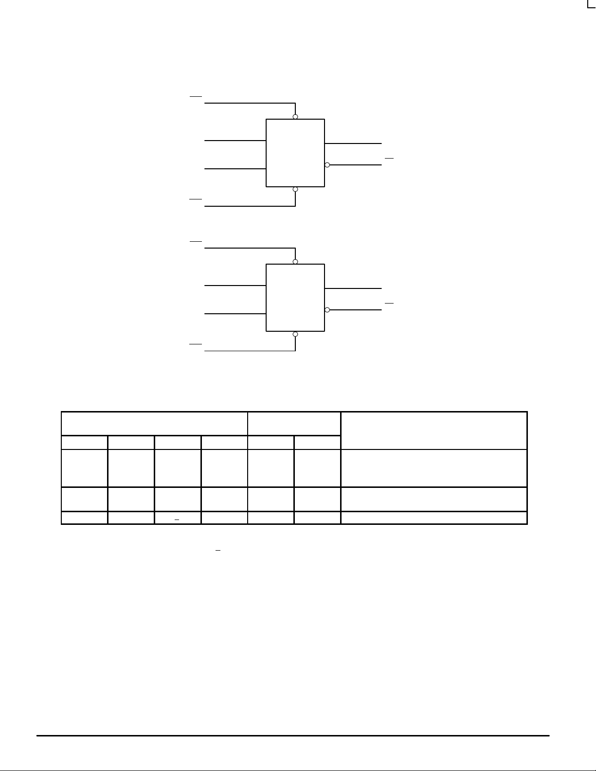
LOGIC DIAGRAM
SD1
CP1 CP
CD1
SD2
CP2 CP
CD2
4
2
D1 D
3
1
10
12
D2 D
11
13
SD
CD
SD
CD
5
Q
Q
Q
Q
O1
6
O1
9
O2
8
O2
INPUTS OUTPUTS
SDn CDn CPn Dn On On
L
H
L L X X H H Undetermined
H
H
H H ↑ X NC NC Hold
H = High Voltage Level; h = High V oltage Level One Setup T ime Prior to the Low–to–High Clock Transition; L = Low Voltage Level; l = Low
Voltage Level One Setup T ime Prior to the Low–to–High Clock T ransition; NC = No Change; X = High or Low Voltage Level or Transitions
are Acceptable; ↑ = Low–to–High Transition; ↑
H
L
H
H
X
X
↑
↑
X
X
h
l
= Not a Low–to–High Transition; For ICC Reasons DO NOT FLOAT Inputs
H
L
H
L
L
H
L
H
OPERATING MODE
Asynchronous Set
Asynchronous Clear
Load and Read Register
MOTOROLA LVQ DATA
2
BR1478
Page 3
MC74LVQ74
ABSOLUTE MAXIMUM RATINGS*
Symbol Parameter Value Condition Unit
V
CC
V
I
V
O
I
IK
I
OK
I
O
I
CC
I
GND
T
STG
* Absolute maximum continuous ratings are those values beyond which damage to the device may occur. Exposure to these conditions or
conditions beyond those indicated may adversely affect device reliability. Functional operation under absolute–maximum–rated conditions is
not implied.
DC Supply Voltage –0.5 to +7.0 V
DC Input Voltage –0.5 ≤ VI ≤ VCC + 0.5V V
DC Output Voltage –0.5 ≤ VO ≤ VCC + 0.5 Output in HIGH or LOW State V
DC Input Diode Current –20 VI = –0.5V mA
+20 VI = VCC + 0.5V mA
DC Output Diode Current –20 VO = –0.5V mA
+20 VI = VCC + 0.5V mA
DC Output Source/Sink Current ±50 mA
DC Supply Current ±200 mA
DC Ground Current ±200 mA
Storage Temperature Range –65 to +150 °C
RECOMMENDED OPERATING CONDITIONS
Symbol Parameter Min Typ Max Unit
V
CC
V
I
V
O
T
A
∆V/∆t Input Transition Rise or Fall Rate, VIN from 0.8V to 2.0V, VCC = 3.0V 0 125 mV/ns
Supply Voltage 2.0 3.3 3.6 V
Input Voltage 0 V
Output Voltage 0 V
Operating Free–Air Temperature –40 +85 °C
CC
CC
V
V
DC ELECTRICAL CHARACTERISTICS
TA = –40°C to +85°C
Symbol Characteristic Condition Min Max Unit
V
IH
V
IL
V
OH
V
OL
I
I
I
OLD
I
OHD
I
CC
1. These values of VI are used to test DC electrical characteristics only. Functional test should use VIH ≥ 2.4V , VIL ≤ 0.5V.
2. Incident wave switching on transmission lines with impedances as low as 75Ω for commercial temperature range is guaranteed. Maximum test
duration is 2ms, one output loaded at a time.
HIGH Level Input Voltage (Note 1) 2.7V ≤ VCC ≤ 3.6V,
LOW Level Input Voltage (Note 1) 2.7V ≤ VCC ≤ 3.6V,
HIGH Level Output Voltage 2.7V ≤ VCC ≤ 3.6V; IOH = –50µA VCC– 0.1 V
LOW Level Output Voltage 2.7V ≤ VCC ≤ 3.6V; IOL = 50µA 0.1 V
Input Leakage Current 2.7V ≤ VCC ≤3.6V; VI= VCC, GND ±1.0 µA
Minimum Dynamic Output Current (Note 2) VCC = 3.6V; V
Quiescent Supply Current 2.7V ≤ VCC ≤3.6V; VI = VCC, GND 10 µA
VO = 0.1V or VCC – 0.1V
VO = 0.1V or VCC – 0.1V
VCC = 2.7V; IOH = –12mA 2.2
VCC = 3.0V; IOH = –12mA 2.48
2.7V ≤ VCC ≤ 3.6V; IOL= 12mA 0.4
= 0.8V Max 36 mA
OLD
VCC = 3.6V; V
= 2.0V Min –25 mA
OHD
2.0 V
0.8 V
LCX DATA
BR1478
3 MOTOROLA
Page 4

MC74LVQ74
DYNAMIC SWITCHING CHARACTERISTICS (VCC = 3.3V)
TA = +25°C
Symbol Characteristic Condition Min Typ Max Unit
V
OLP
V
OLV
V
IHD
V
ILD
1. Number of outputs defined as “n”. Measured with “n–1” outputs switching from HIGH–to–LOW. The remaining output is measured in the
LOW state.
2. Number of data inputs is defined as “n” switching, “n–1” inputs switching 0V to 3.3V.
AC CHARACTERISTICS (tR = tF = 2.5ns; CL = 50pF; RL = 500Ω)
Symbol Parameter Min Typ Max Min Typ Max Min Max Max Unit
f
max
t
PLH
t
PHL
t
PLH
t
PHL
t
OSHL
t
OSLH
1. Skew is defined as the absolute value of the difference between the actual propagation delay for any two separate outputs of the same device.
The specification applies to any outputs switching in the same direction, either HIGH–to–LOW (t
guaranteed by design.
Dynamic LOW Peak Voltage (Note 1) CL = 50pF, VIH = 3.3V, VIL = 0V 0.6 1.0 V
Dynamic LOW Valley Voltage (Note 1) CL = 50pF, VIH = 3.3V, VIL = 0V –0.5 –1.0 V
High Level Dynamic Input Voltage
(Note 2)
Low Level Dynamic Input Voltage
(Note 2)
Maximum Clock Frequency 100 125 55 100 95 MHz
Propagation Delay
CPn to On or On
Propagation Delay
or CDn to On or On
SDn
Output–to–Output Skew
(Note 1)
Input–Under–Test Switching 0V to Threshold,
Input–Under–Test Switching 3.3V to Threshold,
TA = +25°C TA = –40°C to +85°C
VCC = 3.0V to 3.6V VCC = 2.7V VCC = 3.0V to 3.6V VCC = 2.7V
4.5
8.0
6.5
6.5
7.0
1.0
1.0
13.5
12.5
12.0
12.0
1.5
1.5
3.5
3.5
4.0
f=1MHz
f=1MHz
4.5
3.5
4.0
4.0
9.5
7.5
7.5
8.0
1.0
1.0
Limits
17.5
15.0
14.5
15.5
1.5
1.5
4.0
3.5
3.5
3.5
) or LOW–to–HIGH (t
OSHL
1.5 2.0 V
1.5 0.8 V
16.0
14.5
13.0
13.5
1.5
1.5
20.0
18.0
18.0
18.0
1.5
1.5
OSLH
); parameter
ns
ns
ns
AC OPERATING REQUIREMENTS (tR = tF = 2.5ns; CL = 50pF; RL = 500Ω)
Limits
TA = +25°C TA = –40°C to +85°C
VCC = 3.0V to 3.6V VCC = 2.7V VCC = 3.0V to 3.6V VCC = 2.7V
Symbol Parameter Min Min Min Min Unit
t
t
t
t
t
s
h
w
w
rec
Setup TIme, HIGH or LOW Dn to CPn 4.0 5.0 4.5 6.5 ns
Hold TIme, HIGH or LOW Dn to CPn 0.5 0.5 0.5 0.5 ns
SDn or CDn Pulse Width, LOW 5.5 7.0 7.0 10.0 ns
CPn Pulse Width HIGH or LOW 5.5 7.0 7.0 10.0 ns
Recovery Time SDn or CDn to CPn 0.0 0.0 0.0 0.0 ns
CAPACITIVE CHARACTERISTICS
Symbol Parameter Condition Typical Unit
C
PD
C
IN
MOTOROLA LVQ DATA
Power Dissipation Capacitance 10MHz, VCC = 3.3V, VI = 0V or V
Input Capacitance VCC = Open, VI = 0V or V
4
CC
CC
25 pF
4.5 pF
BR1478
Page 5

Dn
CPn
On,
On
MC74LVQ74
V
CC
50% V
CC
50% V
CC
t
PLH
50% V
t
, t
h
f
max
PHL
t
CC
t
s
50% V
CC
0V
V
0V
V
V
CC
OH
OL
w
SDn
CDn
On
On
WAVEFORM 1 – PROPAGATION DELAYS, SETUP AND HOLD TIMES
tR = tF = 2.5ns, 10% to 90%; f = 1MHz; tW = 500ns
50% V
CC
50% V
CC
t
PLH
50% V
CC
50% V
t
PHL
WAVEFORM 2 – PROPAGATION DELAYS
tR = tF = 2.5ns, 10% to 90%; f = 1MHz; tW = 500ns
CC
t
PHL
t
PLH
50% V
50% V
CC
CC
V
0V
V
0V
V
V
CC
CC
OL
OH
LCX DATA
BR1478
SDn
, CDn
CPn
t
50% V
CC
tR = tF = 2.5ns from 10% to 90%; f = 1MHz; tw = 500ns
w
t
rec
WAVEFORM 3 – RECOVERY TIME
Figure 1. AC Waveforms
5 MOTOROLA
50% V
CC
50% V
CC
V
0V
V
0V
CC
CC
Page 6

MC74LVQ74
SDn
, CDn, CPn
CPn
50% V
CC
t
w
t
CC
w
≤
0.8V, VOH ≥ 2.0V
50% V
WAVEFORM 4 – PULSE WIDTH
tR = tF = 2.5ns (or fast as required) from 10% to 90%;
Output requirements: VOL
50% V
50% V
Figure 1. AC Waveforms (continued)
V
CC
CC
CC
V
0V
V
0V
CC
CC
PULSE
GENERATOR
CL = 50pF or equivalent (Includes jig and probe capacitance)
RL = R1 = 500Ω or equivalent
RT = Z
of pulse generator (typically 50Ω)
OUT
DUT
R
T
Figure 2. T est Circuit
C
R
L
L
MOTOROLA LVQ DATA
6
BR1478
Page 7

SEATING
PLANE
MC74LVQ74
OUTLINE DIMENSIONS
D SUFFIX
PLASTIC SOIC PACKAGE
CASE 751A–03
ISSUE F
NOTES:
–A
–
814
–B–P 7 PL
M M
1
G
D 14 PL
0.25 (0.010) T B A
7
X 45°
C
R
K
M
S S
B0.25 (0.010)
M
J
1. DIMENSIONING AND TOLERANCING PER ANSI
Y14.5M, 1982.
2. CONTROLLING DIMENSION: MILLIMETER.
3. DIMENSIONS A AND B DO NOT INCLUDE
MOLD PROTRUSION.
4. MAXIMUM MOLD PROTRUSION 0.15 (0.006)
PER SIDE.
5. DIMENSION D DOES NOT INCLUDE DAMBAR
PROTRUSION. ALLOWABLE DAMBAR
PROTRUSION SHALL BE 0.127 (0.005) TOTAL
IN EXCESS OF THE D DIMENSION AT
MAXIMUM MATERIAL CONDITION.
F
MILLIMETERS INCHES
MIN MINMAX MAX
DIM
A
B
C
D
F
G
J
K
M
P
R
8.75
8.55
4.00
3.80
1.75
1.35
0.49
0.35
1.25
0.40
1.27 BSC 0.050 BSC
0.25
0.19
0.25
0.10
7
0
°
°
5.80
6.20
0.25
0.50
0.337
0.150
0.054
0.014
0.016
0.008
0.004
0.228
0.010
0.344
0.157
0.068
0.019
0.049
0.009
0.009
7
0
°
°
0.244
0.019
14 8
1
Z
D
e
b
0.13 (0.005)
M
HEE
7
A
A
1
0.10 (0.004)
VIEW P
PLASTIC SOIC EIAJ PACKAGE
M SUFFIX
CASE 965–01
ISSUE O
L
E
Q
1
_
M
L
DETAIL P
c
NOTES:
1 DIMENSIONING AND TOLERANCING PER ANSI
Y14.5M, 1982.
2 CONTROLLING DIMENSION: MILLIMETER.
3 DIMENSIONS D AND E DO NOT INCLUDE MOLD
FLASH OR PROTRUSIONS AND ARE MEASURED
AT THE PARTING LINE. MOLD FLASH OR
PROTRUSIONS SHALL NOT EXCEED 0.15 (0.006)
PER SIDE.
4 TERMINAL NUMBERS ARE SHOWN FOR
REFERENCE ONLY.
5 THE LEAD WIDTH DIMENSION (b) DOES NOT
INCLUDE DAMBAR PROTRUSION. ALLOWABLE
DAMBAR PROTRUSION SHALL BE 0.08 (0.003)
TOTAL IN EXCESS OF THE LEAD WIDTH
DIMENSION AT MAXIMUM MATERIAL CONDITION.
DAMBAR CANNOT BE LOCATED ON THE LOWER
RADIUS OR THE FOOT. MINIMUM SPACE
BETWEEN PROTRUSIONS AND ADJACENT LEAD
TO BE 0.46 ( 0.018).
10
_
INCHES
0
_
10
_
MILLIMETERS
DIM MIN MAX MIN MAX
A
--- 2.05 --- 0.081
A
0.05 0.20 0.002 0.008
1
b
0.35 0.50 0.014 0.020
c
0.18 0.27 0.007 0.011
D
9.90 10.50 0.390 0.413
E
5.10 5.45 0.201 0.215
e
1.27 BSC 0.050 BSC
H
7.40 8.20 0.291 0.323
E
L
0.50 0.85 0.020 0.033
L
1.10 1.50 0.043 0.059
E
M
0
_
Q
0.70 0.90 0.028 0.035
1
Z
--- 1.42 --- 0.056
LCX DATA
BR1478
7 MOTOROLA
Page 8

MC74LVQ74
0.076 (0.003)
SEATING
–T–
PLANE
L/2
L
PIN 1
IDENT
0.20 (0.008) T
C
D
K14X REF
0.12 (0.005) V
14 8
A
–V–
M
U
G
OUTLINE DIMENSIONS
SD SUFFIX
PLASTIC SSOP PACKAGE
CASE 940A–03
ISSUE B
M
S
U
T
S
0.25 (0.010)
N
M
B
N
F
71
–U–
S
J
DETAIL E
K
J1
K1
SECTION N–N
–W–
H
DETAIL E
NOTES:
6 DIMENSIONING AND TOLERANCING PER ANSI
Y14.5M, 1982.
7 CONTROLLING DIMENSION: MILLIMETER.
8 DIMENSION A DOES NOT INCLUDE MOLD FLASH,
PROTRUSIONS OR GATE BURRS. MOLD FLASH
OR GATE BURRS SHALL NOT EXCEED 0.15
(0.006) PER SIDE.
9 DIMENSION B DOES NOT INCLUDE INTERLEAD
FLASH OR PROTRUSION. INTERLEAD FLASH OR
PROTRUSION SHALL NOT EXCEED 0.15 (0.006)
PER SIDE.
10 DIMENSION K DOES NOT INCLUDE DAMBAR
PROTRUSION/INTRUSION. ALLOWABLE DAMBAR
PROTRUSION SHALL BE 0.13 (0.005) TOTAL IN
EXCESS OF K DIMENSION AT MAXIMUM
MATERIAL CONDITION. DAMBAR INTRUSION
SHALL NOT REDUCE DIMENSION K BY MORE
THAN 0.07 (0.002) AT LEAST MATERIAL
CONDITION.
11 TERMINAL NUMBERS ARE SHOWN FOR
REFERENCE ONLY.
12 DIMENSION A AND B ARE TO BE DETERMINED
AT DATUM PLANE –W–.
MILLIMETERS
DIMAMIN MAX MIN MAX
6.07 6.33 0.238 0.249
B 5.20 5.38 0.205 0.212
C 1.73 1.99 0.068 0.078
D 0.05 0.21 0.002 0.008
F 0.63 0.95 0.024 0.037
G 0.65 BSC 0.026 BSC
H 1.08 1.22 0.042 0.048
J 0.09 0.20 0.003 0.008
J1 0.09 0.16 0.003 0.006
K 0.25 0.38 0.010 0.015
K1 0.25 0.33 0.010 0.013
L 7.65 7.90 0.301 0.311
M 0 8 0 8
____
INCHES
0.10 (0.004)
SEATING
–T–
PLANE
PLASTIC TSSOP PACKAGE
DT SUFFIX
CASE 948G–01
ISSUE O
S
U
T
S
N
0.25 (0.010)
U0.15 (0.006) T
S
2X L/2
14X REFK
0.10 (0.004) V
14
M
8
M
L
PIN 1
IDENT.
1
S
U0.15 (0.006) T
A
–V–
B
–U–
N
F
7
DETAIL E
K
K1
J
J1
SECTION N–N
C
D
G
H
DETAIL E
NOTES:
1 DIMENSIONING AND TOLERANCING PER ANSI
Y14.5M, 1982.
2 CONTROLLING DIMENSION: MILLIMETER.
3 DIMENSION A DOES NOT INCLUDE MOLD FLASH,
PROTRUSIONS OR GATE BURRS. MOLD FLASH
OR GATE BURRS SHALL NOT EXCEED 0.15
(0.006) PER SIDE.
4 DIMENSION B DOES NOT INCLUDE INTERLEAD
FLASH OR PROTRUSION. INTERLEAD FLASH OR
PROTRUSION SHALL NOT EXCEED
0.25 (0.010) PER SIDE.
5 DIMENSION K DOES NOT INCLUDE DAMBAR
PROTRUSION. ALLOWABLE DAMBAR
PROTRUSION SHALL BE 0.08 (0.003) TOTAL IN
EXCESS OF THE K DIMENSION AT MAXIMUM
MATERIAL CONDITION.
6 TERMINAL NUMBERS ARE SHOWN FOR
REFERENCE ONLY.
7 DIMENSION A AND B ARE TO BE DETERMINED
AT DATUM PLANE –W–.
INCHESMILLIMETERS
–W–
DIM MIN MAX MIN MAX
A 4.90 5.10 0.193 0.200
B 4.30 4.50 0.169 0.177
C ––– 1.20 ––– 0.047
D 0.05 0.15 0.002 0.006
F 0.50 0.75 0.020 0.030
G 0.65 BSC 0.026 BSC
H 0.50 0.60 0.020 0.024
J 0.09 0.20 0.004 0.008
J1 0.09 0.16 0.004 0.006
K 0.19 0.30 0.007 0.012
K1 0.19 0.25 0.007 0.010
L 6.40 BSC 0.252 BSC
M 0 8 0 8
____
MOTOROLA LVQ DATA
8
BR1478
Page 9

MC74LVQ74
Motorola reserves the right to make changes without further notice to any products herein. Motorola makes no warranty , representation or guarantee regarding
the suitability of its products for any particular purpose, nor does Motorola assume any liability arising out of the application or use of any product or circuit, and
specifically disclaims any and all liability, including without limitation consequential or incidental damages. “T ypical” parameters which may be provided in Motorola
data sheets and/or specifications can and do vary in different applications and actual performance may vary over time. All operating parameters, including “Typicals”
must be validated for each customer application by customer’s technical experts. Motorola does not convey any license under its patent rights nor the rights of
others. Motorola products are not designed, intended, or authorized for use as components in systems intended for surgical implant into the body, or other
applications intended to support or sustain life, or for any other application in which the failure of the Motorola product could create a situation where personal injury
or death may occur. Should Buyer purchase or use Motorola products for any such unintended or unauthorized application, Buyer shall indemnify and hold Motorola
and its officers, employees, subsidiaries, affiliates, and distributors harmless against all claims, costs, damages, and expenses, and reasonable attorney fees
arising out of, directly or indirectly, any claim of personal injury or death associated with such unintended or unauthorized use, even if such claim alleges that
Motorola was negligent regarding the design or manufacture of the part. Motorola and are registered trademarks of Motorola, Inc. Motorola, Inc. is an Equal
Opportunity/Affirmative Action Employer.
How to reach us:
USA/EUROPE/Locations Not Listed: Motorola Literature Distribution; JAPAN: Nippon Motorola Ltd.: SPD, Strategic Planning Office, 4–32–1,
P.O. Box 5405, Denver, Colorado 80217. 1–303–675–2140 or 1–800–441–2447 Nishi–Gotanda, Shinagawa–ku, Tokyo 141, Japan. 81–3–5487–8488
Customer Focus Center: 1–800–521–6274
Mfax: RMFAX0@email.sps.mot.com – TOUCHTONE 1–602–244–6609 ASIA/PACIFIC: Motorola Semiconductors H.K. Ltd.; 8B Tai Ping Industrial Park,
Moto rola Fax Back System – US & Canada ONLY 1–800–774–1848 51 Ting Kok Road, Tai Po, N.T., Hong Kong. 852–26629298
HOME PAGE: http://motorola.com/sps/
– http://sps.motorola.com/mfax/
◊
LCX DATA
9 MOTOROLA
Mfax is a trademark of Motorola, Inc.
MC74LVQ74/D
BR1478
 Loading...