

Page 1
SEMICONDUCTOR TECHNICAL DATA
&-&$* *$
")*( (%)",( "*!
+$ +*'+* % $&#
%$)
"*! &$(%* %'+*) % +*'+*)
** &%%,(*"%
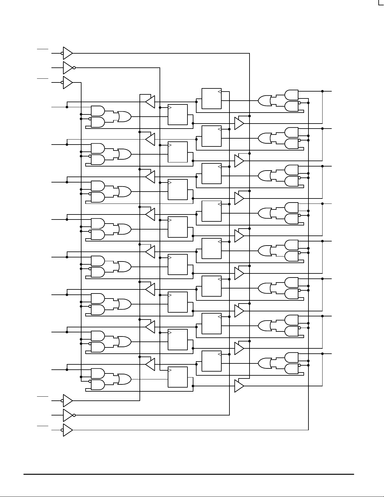
The MC74LCX2952 is a high performance, non–inverting octal
registered transceiver operating from a 2.7 to 3.6V supply. High
impedance TTL compatible inputs significantly reduce current loading to
input drivers while TTL compatible outputs offer improved switching noise
performance. A VI specification of 5.5V allows MC74LCX2952 inputs to
be safely driven from 5V devices. The MC74LCX2952 is suitable for
memory address driving and all TTL level bus oriented transceiver
applications.
Two 8–bit back to back registers store data from either of two
bidirectional buses. Data applied to the inputs is entered and stored on
the rising edge of the Clock (CAB, CBA) provided that the Clock Enable
(CEAB
, CEBA) is Low. The data is then presented at the 3–state output
buffers, but is only accessible when the Output Enable (OEAB
Low. The operation of the MC74LCX2952 is symmetrical — A inputs to B
outputs occurs in the same manner as B inputs to A outputs.
, OEBA) is
LOW–VOLTAGE CMOS
OCTAL REGISTERED
TRANSCEIVER
DW SUFFIX
24–LEAD PLASTIC SOIC WIDE PACKAGE
CASE 751E–04
• Designed for 2.7 to 3.6V V
Operation
CC
• 5V Tolerant — Interface Capability With 5V TTL Logic
• Supports Live Insertion and Withdrawal
• I
Specification Guarantees High Impedance When VCC = 0V
OFF
• LVTTL Compatible
• LVCMOS Compatible
• 24mA Balanced Output Sink and Source Capability
• Near Zero Static Supply Current in All Three Logic States (10µA)
Substantially Reduces System Power Requirements
• Latchup Performance Exceeds 500mA
• ESD Performance: Human Body Model >2000V; Machine Model >200V
V
A7 A6 A5 A4 A3 A2 A1 A0 OEBA
CC
2324 22 21 20 19 18
21 34567
B7 B6 B5 B4 B3 B2 B1 B0 OEAB CAB
Figure 1. 24–Lead Pinout (Top View)
17
16
9
8
15
10
CEAB GND
CBA CEBA
14
13
11
12
24–LEAD PLASTIC SSOP PACKAGE
24–LEAD PLASTIC TSSOP PACKAGE
PIN NAMES
Pins
A0–A7
B0–B7
CAB, CBA
CEAB
, CEBA
OEAB, OEBA
SD SUFFIX
CASE 940D–03
DT SUFFIX
CASE 948H–01
Function
Side A Inputs/Outputs
Side B Inputs/Outputs
Clock Pulse Inputs
Clock Enable Inputs
Output Enable Inputs
3/97
Motorola, Inc. 1997
1
REV 1
Page 2
MC74LCX2952
9
OEAB
10
CAB
11
CEAB
16
A0
17
A1
18
A2
19
A3
20
A4
21
A5
22
A6
23
A7
8
C
Q
C
Q
D
C
Q
D
C
Q
D
C
Q
D
C
Q
D
C
Q
D
C
Q
D
C
Q
D
D
C
Q
D
C
Q
D
C
Q
D
C
Q
D
C
Q
D
C
Q
D
C
Q
D
B0
7
B1
6
B2
5
B3
4
B4
3
B5
2
B6
1
B7
15
OEBA
14
CBA
13
CEBA
Figure 2. Logic Diagram
MOTOROLA LCX DATA
2
BR1339 — REV 3
Page 3
MC74LCX2952
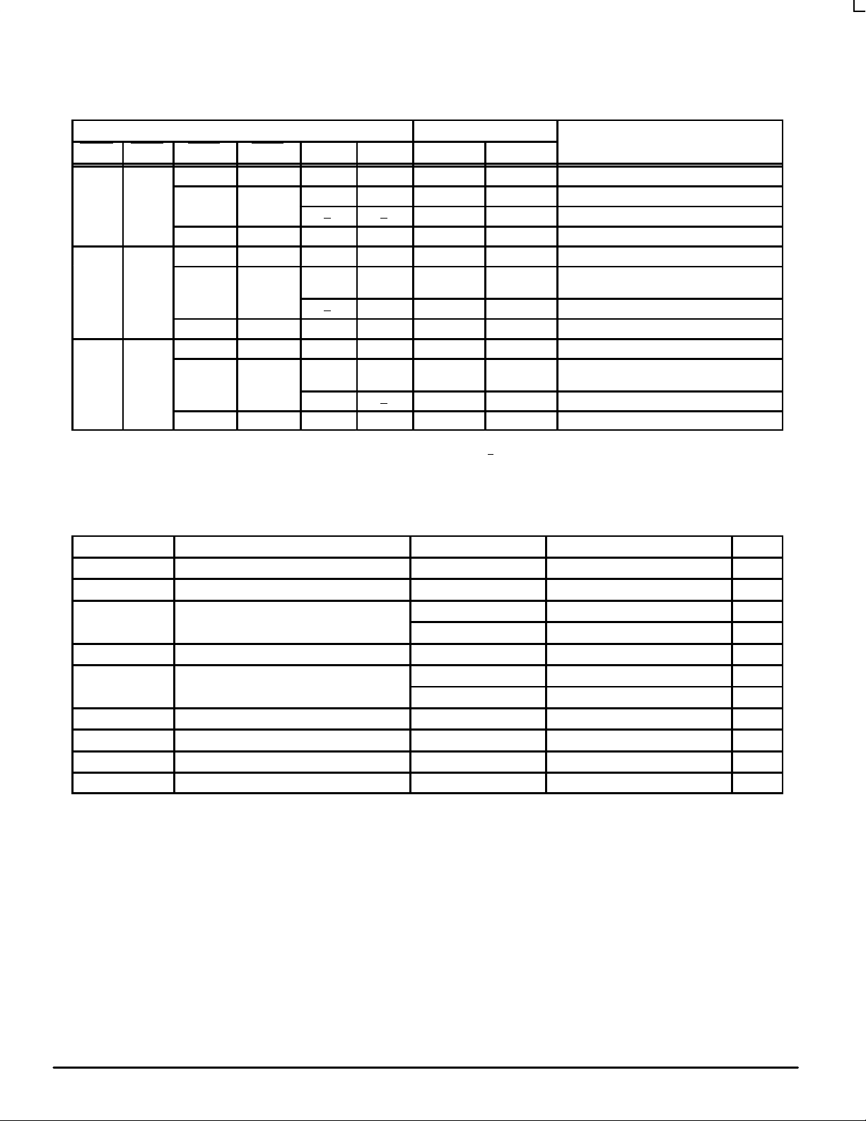
O
FUNCTION TABLE
Inputs
OEAB OEBA CEAB CEBA CAB CBA An Bn
H H Input Input
l l ↑ ↑ X X Load Register; Disable Outputs
↑ ↑ X X Hold; Disable Outputs
h h X X X X Hold; Disable Outputs
L H Input Output
l X ↑ X l
↑ X X QA Hold; Read B Output
h X X X X QA Hold; Read B Output
H L Output Input
X l X ↑ L
X ↑ QB X Hold; Read A Output
X h X X QB X Hold; Read A Output
H = High Voltage Level; h = High Voltage Level One Setup Time Prior to the Low–to–High Clock Transition; L = Low Voltage Level; l = Low Voltage Level One Setup
Time Prior to the Low–to–High Clock T ransition; X = Don’t Care; ↑ = Low–to–High Clock Transition; ↑
QB = B input storage register; * = The clocks are not internally gated with either the Output Enables or the Source Inputs. Therefore, data at the A or B ports may be
clocked into the storage registers, at any time. For ICC reasons, Do Not Float Inputs.
Data Ports
h
H
perating Mode
L
H
l
h
= NOT Low–to–High Clock Transition; QA = A input storage register;
Load A to B Register; Read B Output
Load B to A Register; Read A Output
ABSOLUTE MAXIMUM RATINGS*
Symbol Parameter Value Condition Unit
V
CC
V
I
V
O
I
IK
I
OK
I
O
I
CC
I
GND
T
STG
* Absolute maximum continuous ratings are those values beyond which damage to the device may occur. Exposure to these conditions or
conditions beyond those indicated may adversely affect device reliability. Functional operation under absolute–maximum–rated conditions is
not implied.
1. Output in HIGH or LOW State. IO absolute maximum rating must be observed.
DC Supply Voltage –0.5 to +7.0 V
DC Input Voltage –0.5 ≤ VI ≤ +7.0 V
DC Output Voltage –0.5 ≤ VO ≤ +7.0 Output in 3–State V
–0.5 ≤ VO ≤ VCC + 0.5 Note 1. V
DC Input Diode Current –50 VI < GND mA
DC Output Diode Current –50 VO < GND mA
+50 VO > V
DC Output Source/Sink Current ±50 mA
DC Supply Current Per Supply Pin ±100 mA
DC Ground Current Per Ground Pin ±100 mA
Storage Temperature Range –65 to +150 °C
CC
mA
LCX DATA
BR1339 — REV 3
3 MOTOROLA
Page 4

MC74LCX2952
RECOMMENDED OPERATING CONDITIONS
Symbol Parameter Min Typ Max Unit
V
CC
V
I
V
O
I
OH
I
OL
I
OH
I
OL
T
A
∆t/∆V Input Transition Rise or Fall Rate, VIN from 0.8V to 2.0V ,
DC ELECTRICAL CHARACTERISTICS
Symbol Characteristic Condition Min Max Unit
V
IH
V
IL
V
OH
V
OL
I
I
I
OZ
I
OFF
I
CC
∆I
CC
2. These values of VI are used to test DC electrical characteristics only.
HIGH Level Input Voltage (Note 2.) 2.7V ≤ VCC ≤ 3.6V 2.0 V
LOW Level Input Voltage (Note 2.) 2.7V ≤ VCC ≤ 3.6V 0.8 V
HIGH Level Output Voltage 2.7V ≤ VCC ≤ 3.6V; IOH = –100µA VCC– 0.2 V
LOW Level Output Voltage 2.7V ≤ VCC ≤ 3.6V; IOL = 100µA 0.2 V
Input Leakage Current 2.7V ≤ VCC ≤ 3.6V; 0V ≤ VI ≤ 5.5V ±5.0 µA
3–State Output Current 2.7 ≤ VCC ≤ 3.6V; 0V ≤ VO ≤ 5.5V;
Power–Off Leakage Current VCC = 0V; VI or VO = 5.5V 10 µA
Quiescent Supply Current
Increase in ICC per Input 2.7 ≤ VCC ≤ 3.6V; VIH = VCC – 0.6V 500 µA
Supply Voltage Operating
Data Retention Only
Input Voltage 0 5.5 V
Output Voltage (HIGH or LOW State)
(3–State)
HIGH Level Output Current, VCC = 3.0V – 3.6V –24 mA
LOW Level Output Current, VCC = 3.0V – 3.6V 24 mA
HIGH Level Output Current, VCC = 2.7V – 3.0V –12 mA
LOW Level Output Current, VCC = 2.7V – 3.0V 12 mA
Operating Free–Air Temperature –40 +85 °C
VCC = 3.0V
VCC = 2.7V; IOH = –12mA 2.2
VCC = 3.0V; IOH = –18mA 2.4
VCC = 3.0V; IOH = –24mA 2.2
VCC = 2.7V; IOL= 12mA 0.4
VCC = 3.0V; IOL = 16mA 0.4
VCC = 3.0V; IOL = 24mA 0.55
VI = VIH or V
2.7 ≤ VCC ≤ 3.6V; VI = GND or V
2.7 ≤ VCC ≤ 3.6V; 3.6 ≤ VI or VO ≤ 5.5V ±10 µA
2.0
1.5
0
0
0 10 ns/V
IL
CC
3.3
3.3
TA = –40°C to +85°C
3.6
3.6
V
CC
5.5
±5.0 µA
10 µA
V
V
MOTOROLA LCX DATA
4
BR1339 — REV 3
Page 5

MC74LCX2952
AC CHARACTERISTICS (Note 3.; tR = tF = 2.5ns; CL = 50pF; RL = 500Ω)
Limits
TA = –40°C to +85°C
VCC = 3.0V to 3.6V VCC = 2.7V
Symbol Parameter Waveform Min Max Min Max Unit
f
max
t
PLH
t
PHL
t
PZH
t
PZL
t
PHZ
t
PLZ
t
s
t
h
t
s
t
h
t
w
t
OSHL
t
OSLH
3. These AC parameters are preliminary and may be modified prior to release. The maximum AC limits are design targets. Actual performance
will be specified upon completion of characterization.
4. Skew is defined as the absolute value of the difference between the actual propagation delay for any two separate outputs of the same device.
The specification applies to any outputs switching in the same direction, either HIGH–to–LOW (t
guaranteed by design.
Clock Pulse Frequency 3 150 MHz
Propagation Delay
Clock to Output
Output Enable Time to
High and Low Level
Output Disable Time From
High and Low Level
Setup Time, HIGH to LOW Data to Clock 3 2.5 2.5 ns
Hold Time, HIGH to LOW Data to Clock 3 1.5 1.5 ns
Setup Time, HIGH to LOW CExx to Clock 3 2.5 2.5 ns
Hold Time, HIGH to LOW CExx to Clock 3 1.5 1.5 ns
Clock Pulse Width, HIGH or LOW 3 3.3 3.3 ns
Output–to–Output Skew
(Note 4.)
1 1.5
1.5
2 1.5
1.5
2 1.5
1.5
8.0
8.0
8.0
8.0
6.0
6.0
1.0
1.0
) or LOW–to–HIGH (t
OSHL
1.5
1.5
1.5
1.5
1.5
1.5
9.0
9.0
9.0
9.0
7.0
7.0
OSLH
ns
ns
ns
ns
); parameter
DYNAMIC SWITCHING CHARACTERISTICS
TA = +25°C
Symbol Characteristic Condition Min Typ Max Unit
V
OLP
V
OLV
5. Number of outputs defined as “n”. Measured with “n–1” outputs switching from HIGH–to–LOW or LOW–to–HIGH. The remaining output is
measured in the LOW state.
Dynamic LOW Peak Voltage (Note 5.) VCC = 3.3V, CL = 50pF, VIH = 3.3V, VIL = 0V 0.8 V
Dynamic LOW Valley Voltage (Note 5.) VCC = 3.3V, CL = 50pF, VIH = 3.3V, VIL = 0V 0.8 V
CAPACITIVE CHARACTERISTICS
Symbol Parameter Condition Typical Unit
C
IN
C
I/O
C
PD
Input Capacitance VCC = 3.3V, VI = 0V or V
Input/Output Capacitance VCC = 3.3V, VI = 0V or V
Power Dissipation Capacitance 10MHz, VCC = 3.3V, VI = 0V or V
CC
CC
CC
7 pF
8 pF
25 pF
LCX DATA
BR1339 — REV 3
5 MOTOROLA
Page 6

MC74LCX2952
CAB,
CBA
Bn, An
1.5V
t
, t
PLH
PHL
1.5V
WAVEFORM 1 – Cxx to An/Bn PROPAGATION DELAYS
tR = tF = 2.5ns, 10% to 90%; f = 1MHz; tW = 500ns
2.7V
0V
V
OH
V
OL
OEAB
OEBA
An, Bn
Bn, An
,
1.5V1.5V
t
PZH
1.5V
t
PZL
1.5V
WAVEFORM 2 – OExx to An/Bn OUTPUT ENABLE AND DISABLE TIMES
An, Bn,
CEAB
,
CEBA
CAB,
CBA
tR = tF = 2.5ns, 10% to 90%; f = 1MHz; tW = 500ns
t
s
1.5V 1.5V
t
PHZ
t
PLZ
1.5V
t
h
t
w
f
max
2.7V
0V
VOH – 0.3V
VOL + 0.3V
2.7V
0V
2.7V
0V
≈
0V
≈
3V
WAVEFORM 3 – Cxx MINIMUM PULSE WIDTH, An/Bn/CExx
SETUP AND HOLD TIMES
tR = tF = 2.5ns, 10% to 90%; f = 1MHz; tW = 500ns except when noted
to Cxx
Figure 3. AC Waveforms
MOTOROLA LCX DATA
6
BR1339 — REV 3
Page 7

NEGATIVE
PULSE
1.5V
MC74LCX2952
t
w
1.5V
PULSE
GENERATOR
POSITIVE
PULSE
1.5V
t
w
WAVEFORM 4 – INPUT PULSE DEFINITION
tR = tF = 2.5ns, 10% to 90% of 0V to 2.7V
1.5V
Figure 4. AC Waveforms (continued)
V
CC
DUT
R
T
TEST SWITCH
t
, t
PLH
PHL
t
, t
PZL
PLZ
Open Collector/Drain t
t
, t
PZH
PHZ
CL = 50pF or equivalent (Includes jig and probe capacitance)
RL = R1 = 500Ω or equivalent
RT = Z
of pulse generator (typically 50Ω)
OUT
PLH
and t
PHL
C
L
Open
GND
R
6V
6V
6V
R
1
L
OPEN
GND
LCX DATA
BR1339 — REV 3
Figure 5. T est Circuit
7 MOTOROLA
Page 8

MC74LCX2952
24 13
112
D 24 PL
–T
–
SEATING
PLANE
–A
–
0.010 (0.25) A B
M
S S
T
G 22 PL
OUTLINE DIMENSIONS
DW SUFFIX
PLASTIC SOIC PACKAGE
CASE 751E–04
ISSUE E
–B
P 12 PL
–
C
K
0.010 (0.25)
J
F
M
M M
B
R X 45°
NOTES:
1. DIMENSIONING AND TOLERANCING PER
ANSI Y14.5M, 1982.
2. CONTROLLING DIMENSION: MILLIMETER.
3. DIMENSIONS A AND B DO NOT INCLUDE
MOLD PROTRUSION.
4. MAXIMUM MOLD PROTRUSION 0.15
(0.006) PER SIDE.
5. DIMENSION D DOES NOT INCLUDE
DAMBAR PROTRUSION. ALLOWABLE
DAMBAR PROTRUSION SHALL BE 0.13
(0.005) TOTAL IN EXCESS OF D
DIMENSION AT MAXIMUM MATERIAL
CONDITION.
MILLIMETERS INCHES
MIN MINMAX MAX
DIM
G
M
A
B
C
D
F
J
K
P
R
15.54
7.60
2.65
0.49
0.90
0.32
0.29
8
10.55
0.75
0.601
0.292
0.093
0.014
0.016
0.009
0.005
0
°
°
0.395
0.010
15.25
7.40
2.35
0.35
0.41
1.27 BSC 0.050 BSC
0.23
0.13
0
°
10.05
0.25
0.612
0.299
0.104
0.019
0.035
0.013
0.011
8
°
0.415
0.029
0.076 (0.003)
SEATING
–T–
PLANE
L/2
L
PIN 1
IDENT
0.20 (0.008) T
C
D
K24X REF
0.12 (0.005) V
24 13
A
–V–
M
S
U
G
H
SD SUFFIX
PLASTIC SSOP PACKAGE
CASE 940D–03
ISSUE B
M
121
S
U
T
S
J
B
SECTION N–N
–U–
N
N
DETAIL E
DETAIL E
K
K1
0.25 (0.010)
M
F
J1
–W–
NOTES:
1 DIMENSIONING AND TOLERANCING PER ANSI
Y14.5M, 1982.
2 CONTROLLING DIMENSION: MILLIMETER.
3 DIMENSION A DOES NOT INCLUDE MOLD FLASH,
PROTRUSIONS OR GATE BURRS. MOLD FLASH
OR GATE BURRS SHALL NOT EXCEED 0.15
(0.006) PER SIDE.
4 DIMENSION B DOES NOT INCLUDE INTERLEAD
FLASH OR PROTRUSION. INTERLEAD FLASH OR
PROTRUSION SHALL NOT EXCEED 0.15 (0.006)
PER SIDE.
5 DIMENSION K DOES NOT INCLUDE DAMBAR
PROTRUSION/INTRUSION. ALLOWABLE DAMBAR
PROTRUSION SHALL BE 0.13 (0.005) TOTAL IN
EXCESS OF K DIMENSION AT MAXIMUM
MATERIAL CONDITION. DAMBAR INTRUSION
SHALL NOT REDUCE DIMENSION K BY MORE
THAN 0.07 (0.002) AT LEAST MATERIAL
CONDITION.
6 TERMINAL NUMBERS ARE SHOWN FOR
REFERENCE ONLY.
7 DIMENSION A AND B ARE TO BE DETERMINED
AT DATUM PLANE –W–.
MILLIMETERS
DIMAMIN MAX MIN MAX
8.07 8.33 0.317 0.328
B 5.20 5.38 0.205 0.212
C 1.73 1.99 0.068 0.078
D 0.05 0.21 0.002 0.008
F 0.63 0.95 0.024 0.037
G 0.65 BSC 0.026 BSC
H 0.44 0.60 0.017 0.024
J 0.09 0.20 0.003 0.008
J1 0.09 0.16 0.003 0.006
K 0.25 0.38 0.010 0.015
K1 0.25 0.33 0.010 0.013
L 7.65 7.90 0.301 0.311
M 0 8 0 8
____
INCHES
MOTOROLA LCX DATA
8
BR1339 — REV 3
Page 9

S
U0.15 (0.006) T
S
U0.15 (0.006) T
0.10 (0.004)
SEATING
–T–
PLANE
MC74LCX2952
OUTLINE DIMENSIONS
DT SUFFIX
PLASTIC TSSOP PACKAGE
CASE 948H–01
ISSUE O
24X REFK
M
2X L/2
0.10 (0.004) V
24
L
PIN 1
IDENT.
1
A
–V–
C
D
G
S
U
T
S
NOTES:
1 DIMENSIONING AND TOLERANCING PER ANSI
13
B
–U–
12
H
–W–
Y14.5M, 1982.
2 CONTROLLING DIMENSION: MILLIMETER.
3 DIMENSION A DOES NOT INCLUDE MOLD FLASH,
PROTRUSIONS OR GATE BURRS. MOLD FLASH
OR GATE BURRS SHALL NOT EXCEED 0.15
(0.006) PER SIDE.
4 DIMENSION B DOES NOT INCLUDE INTERLEAD
FLASH OR PROTRUSION. INTERLEAD FLASH OR
PROTRUSION SHALL NOT EXCEED
0.25 (0.010) PER SIDE.
5 DIMENSION K DOES NOT INCLUDE DAMBAR
PROTRUSION. ALLOWABLE DAMBAR
PROTRUSION SHALL BE 0.08 (0.003) TOTAL IN
EXCESS OF THE K DIMENSION AT MAXIMUM
MATERIAL CONDITION.
6 TERMINAL NUMBERS ARE SHOWN FOR
REFERENCE ONLY.
7 DIMENSION A AND B ARE TO BE DETERMINED
AT DATUM PLANE –W–.
DIM MIN MAX MIN MAX
A 7.70 7.90 0.303 0.311
B 4.30 4.50 0.169 0.177
C ––– 1.20 ––– 0.047
D 0.05 0.15 0.002 0.006
F 0.50 0.75 0.020 0.030
G 0.65 BSC 0.026 BSC
H 0.27 0.37 0.011 0.015
J 0.09 0.20 0.004 0.008
J1 0.09 0.16 0.004 0.006
K 0.19 0.30 0.007 0.012
K1 0.19 0.25 0.007 0.010
L 6.40 BSC 0.252 BSC
M 0 8 0 8
____
INCHESMILLIMETERS
DETAIL E
K
N
K1
J1
SECTION N–N
J
N
F
DETAIL E
0.25 (0.010)
M
LCX DATA
BR1339 — REV 3
9 MOTOROLA
Page 10

MC74LCX2952
Motorola reserves the right to make changes without further notice to any products herein. Motorola makes no warranty , representation or guarantee regarding
the suitability of its products for any particular purpose, nor does Motorola assume any liability arising out of the application or use of any product or circuit, and
specifically disclaims any and all liability, including without limitation consequential or incidental damages. “T ypical” parameters which may be provided in Motorola
data sheets and/or specifications can and do vary in different applications and actual performance may vary over time. All operating parameters, including “Typicals”
must be validated for each customer application by customer’s technical experts. Motorola does not convey any license under its patent rights nor the rights of
others. Motorola products are not designed, intended, or authorized for use as components in systems intended for surgical implant into the body, or other
applications intended to support or sustain life, or for any other application in which the failure of the Motorola product could create a situation where personal injury
or death may occur. Should Buyer purchase or use Motorola products for any such unintended or unauthorized application, Buyer shall indemnify and hold Motorola
and its officers, employees, subsidiaries, affiliates, and distributors harmless against all claims, costs, damages, and expenses, and reasonable attorney fees
arising out of, directly or indirectly, any claim of personal injury or death associated with such unintended or unauthorized use, even if such claim alleges that
Motorola was negligent regarding the design or manufacture of the part. Motorola and are registered trademarks of Motorola, Inc. Motorola, Inc. is an Equal
Opportunity/Affirmative Action Employer.
How to reach us:
USA/EUROPE/Locations Not Listed: Motorola Literature Distribution; JAP AN: Nippon Motorola Ltd.; Tatsumi–SPD–JLDC, 6F Seibu–Butsuryu–Center,
P.O. Box 5405, Denver, Colorado 80217. 303–675–2140 or 1–800–441–2447 3–14–2 T atsumi Koto–Ku, Tokyo 135, Japan. 81–3–3521–8315
Mfax: RMFAX0@email.sps.mot.com – TOUCHTONE 602–244–6609 ASIA/PACIFIC: Motorola Semiconductors H.K. Ltd.; 8B Tai Ping Industrial Park,
INTERNET: http://www.mot.com/SPS/
– US & Canada ONLY 1–800–774–1848 51 Ting Kok Road, Tai Po, N.T., Hong Kong. 852–26629298
◊
MOTOROLA LCX DATA
10
Mfax is a trademark of Motorola, Inc.
MC74LCX2952/D
BR1339 — REV 3
 Loading...