

Page 1
SEMICONDUCTOR TECHNICAL DATA
1
REV 6
Motorola, Inc. 1995
10/95
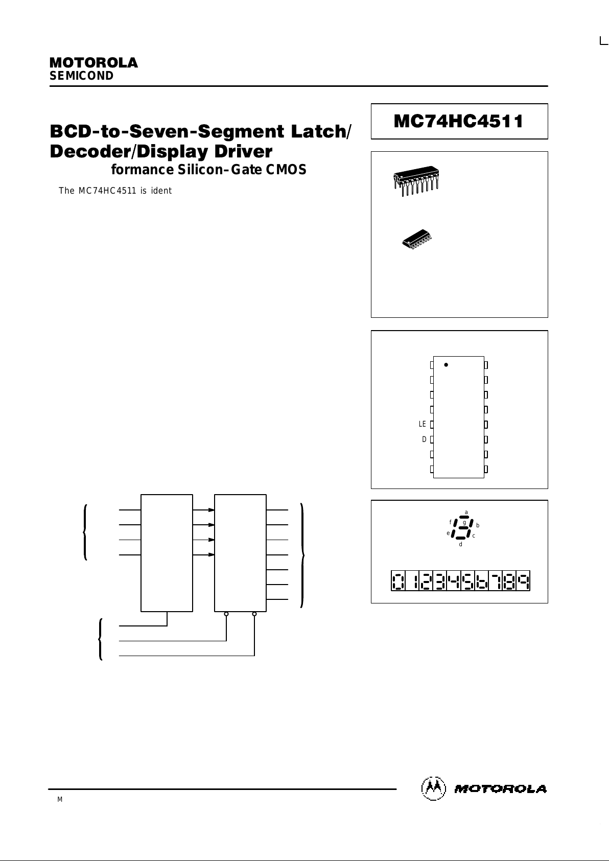
!"! !
# "
High–Performance Silicon–Gate CMOS
The MC74HC4511 is identical in pinout t o the MC14511 metal–gate
CMOS d ecoder/driver. The device inputs are c ompatible with standard
CMOS outputs; with pullup resistors, they are compatible with LSTTL
outputs.
The HC4511 provides the functions of a 4–bit storage latch, a BCD–to–
seven–segment decoder, and a display driver. It can be used either directly
or indirectly with seven–segment light–emitting diode (LED), incandescent,
fluorescent, g as discharge, or liquid–crystal readouts. Lamp test (LT),
blanking (BI), and latch enable (LE) inputs are used to test the display , to turn
off or pulse modulate the brightness of the display , and to store a BCD code,
respectively.
• Latch Storage of BCD Inputs
• Blanking Input
• Lamp Test Input
• Output Drive Capability: 10 LSTTL Loads
• Outputs Directly Interface to CMOS, NMOS, and TTL
• Operating Voltage Range: 2 to 6 V
• Low Input Current: 1 µA
• High Noise Immunity Characteristic of CMOS Devices
• In Compliance with the Requirements Defined by JEDEC Standard
No. 7A
• Chip Complexity: 264 FETs or 66 Equivalent Gates
LOGIC DIAGRAM
4–BIT
TRANSPARENT
LATCH
DECODER
AND
OUTPUT
CONTROL
7
1
2
6
13
12
11
10
9
15
14
D (MSB)
C
B
A (LSB) a
b
c
d
e
f
g
5
4
3
LT
BI
LE
PIN 16 = V
CC
PIN 8 = GND
BCD
INPUTS
CONTROL
INPUTS
SEVEN–
SEGMENT
DISPLAY–
DRIVER
OUTPUTS
PIN ASSIGNMENT
13
14
15
16
9
10
11
125
4
3
2
1
8
7
6
b
a
g
f
V
CC
e
d
c
BI
LT
C
B
GND
A
D
LE
a
b
c
d
e
f g
DISPLAY
D SUFFIX
SOIC PACKAGE
CASE 751B–05
N SUFFIX
PLASTIC PACKAGE
CASE 648–08
1
16
1
16
ORDERING INFORMATION
MC74HCXXXXN
MC74HCXXXXD
Plastic
SOIC
Page 2
MC74HC4511
MOTOROLA High–Speed CMOS Logic Data
DL129 — Rev 6
2
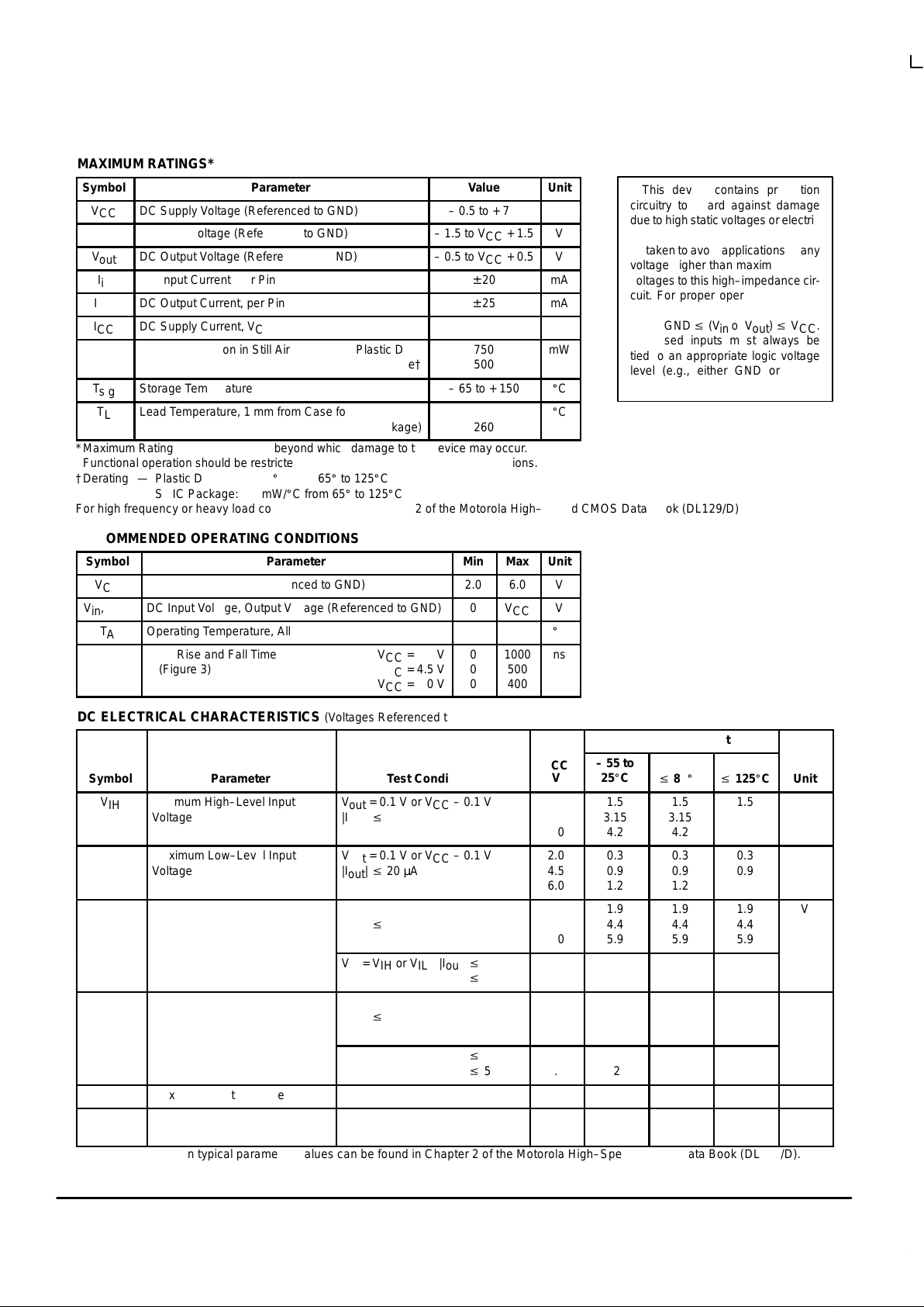
MAXIMUM RATINGS*
Symbol
Parameter
Value
Unit
V
CC
DC Supply Voltage (Referenced to GND)
– 0.5 to + 7.0
V
V
in
DC Input Voltage (Referenced to GND)
– 1.5 to VCC + 1.5
V
V
out
DC Output Voltage (Referenced to GND)
– 0.5 to VCC + 0.5
V
I
in
DC Input Current, per Pin
± 20
mA
I
out
DC Output Current, per Pin
± 25
mA
I
CC
DC Supply Current, VCC and GND Pins
± 70
mA
P
D
Power Dissipation in Still Air Plastic DIP†
SOIC Package†
750
500
mW
T
stg
Storage Temperature
– 65 to + 150
_
C
T
L
Lead Temperature, 1 mm from Case for 10 Seconds
(Plastic DIP or SOIC Package)
260
_
C
*Maximum Ratings are those values beyond which damage to the device may occur.
Functional operation should be restricted to the Recommended Operating Conditions.
†Derating — Plastic DIP: – 10 mW/_C from 65_ to 125_C
SOIC Package: – 7 mW/_C from 65_ to 125_C
For high frequency or heavy load considerations, see Chapter 2 of the Motorola High–Speed CMOS Data Book (DL129/D).
RECOMMENDED OPERATING CONDITIONS
Symbol
Parameter
Min
Max
Unit
V
CC
DC Supply Voltage (Referenced to GND)
2.0
6.0
V
Vin, V
out
DC Input Voltage, Output Voltage (Referenced to GND)
0
V
CC
V
T
A
Operating Temperature, All Package Types
– 55
+ 125
_
C
tr, t
f
Input Rise and Fall Time VCC = 2.0 V
(Figure 3) VCC = 4.5 V
VCC = 6.0 V
0
0
0
1000
500
400
ns
DC ELECTRICAL CHARACTERISTICS (Voltages Referenced to GND)
Guaranteed Limit
Symbol
Parameter
Test Conditions
V
CC
V
– 55 to
25_C
v
85_Cv 125_C
Unit
V
IH
Minimum High–Level Input
Voltage
V
out
= 0.1 V or VCC – 0.1 V
|I
out
| v 20 µA
2.0
4.5
6.0
1.5
3.15
4.2
1.5
3.15
4.2
1.5
3.15
4.2
V
V
IL
Maximum Low–Level Input
Voltage
V
out
= 0.1 V or VCC – 0.1 V
|I
out
| v 20 µA
2.0
4.5
6.0
0.3
0.9
1.2
0.3
0.9
1.2
0.3
0.9
1.2
V
V
OH
Minimum High–Level Output
Voltage
Vin = VIH or V
IL
|I
out
| v 20 µA
2.0
4.5
6.0
1.9
4.4
5.9
1.9
4.4
5.9
1.9
4.4
5.9
V
Vin = VIH or VIL|I
out
| v 6.0 mA
|I
out
| v 7.8 mA
4.5
6.0
3.98
5.48
3.84
5.34
3.70
5.20
V
OL
Maximum Low–Level Output
Voltage
Vin = VIH or V
IL
|I
out
| v 20 µA
2.0
4.5
6.0
0.1
0.1
0.1
0.1
0.1
0.1
0.1
0.1
0.1
V
Vin = VIH or VIL|I
out
| v 4.0 mA
|I
out
| v 5.2 mA
4.5
6.0
0.26
0.26
0.33
0.33
0.40
0.40
I
in
Maximum Input Leakage Current
Vin = VCC or GND
6.0
± 0.1
± 1.0
± 1.0
µA
I
CC
Maximum Quiescent Supply
Current (per Package)
Vin = VCC or GND
I
out
= 0 µA
6.0
8
80
160
µA
NOTE: Information on typical parametric values can be found in Chapter 2 of the Motorola High–Speed CMOS Data Book (DL129/D).
This device contains protection
circuitry to guard against damage
due to high static voltages or electric
fields. However, precautions must
be taken to avoid applications of any
voltage higher than maximum rated
voltages to this high–impedance circuit. For proper operation, Vin and
V
out
should be constrained to the
range GND v (Vin or V
out
) v VCC.
Unused inputs must always be
tied to an appropriate logic voltage
level (e.g., either GND or VCC).
Unused outputs must be left open.
Page 3
MC74HC4511
High–Speed CMOS Logic Data
DL129 — Rev 6
3 MOTOROLA
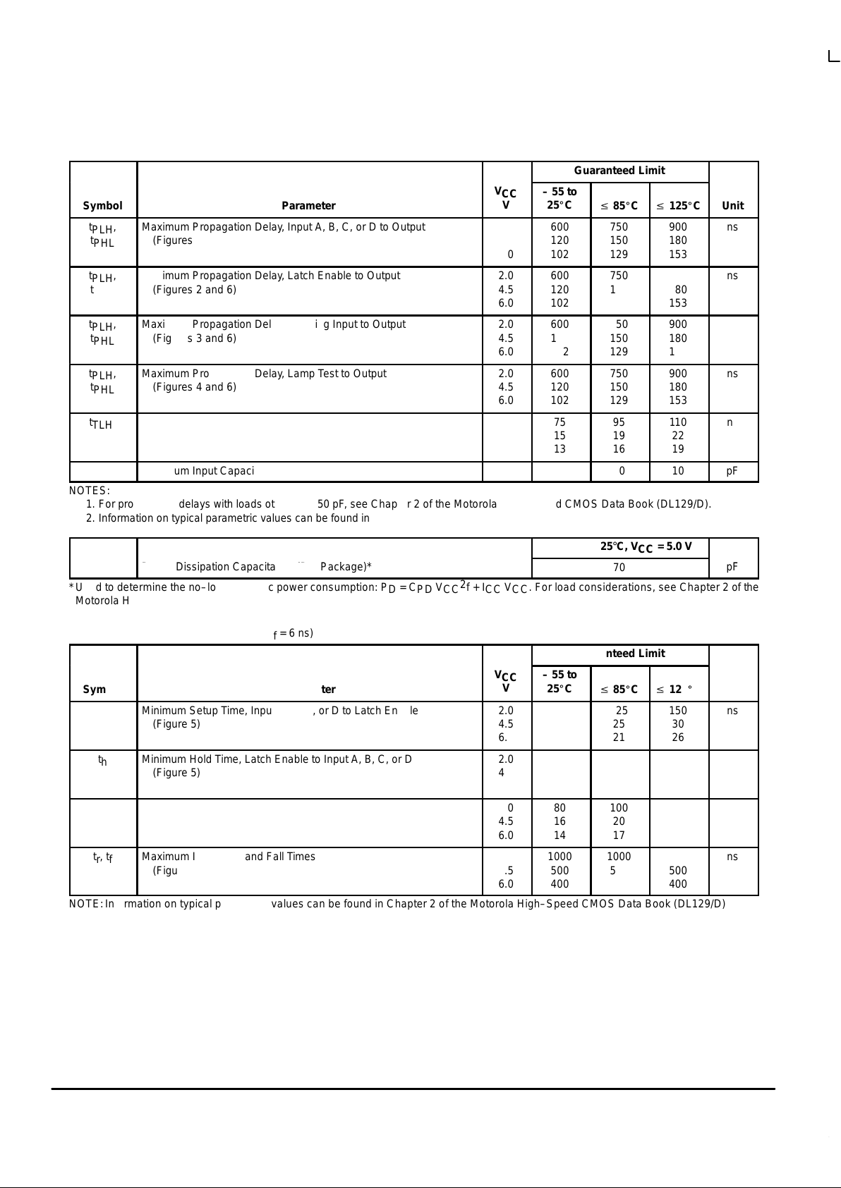
AC ELECTRICAL CHARACTERISTICS (C
L
= 50 pF, Input tr = tf = 6 ns)
Guaranteed Limit
Symbol
Parameter
V
CC
V
– 55 to
25_C
v
85_Cv 125_C
Unit
t
PLH
,
t
PHL
Maximum Propagation Delay, Input A, B, C, or D to Output
(Figures 1 and 6)
2.0
4.5
6.0
600
120
102
750
150
129
900
180
153
ns
t
PLH
,
t
PHL
Maximum Propagation Delay, Latch Enable to Output
(Figures 2 and 6)
2.0
4.5
6.0
600
120
102
750
150
129
900
180
153
ns
t
PLH
,
t
PHL
Maximum Propagation Delay, Blanking Input to Output
(Figures 3 and 6)
2.0
4.5
6.0
600
120
102
750
150
129
900
180
153
ns
t
PLH
,
t
PHL
Maximum Propagation Delay, Lamp Test to Output
(Figures 4 and 6)
2.0
4.5
6.0
600
120
102
750
150
129
900
180
153
ns
t
TLH
,
t
THL
Maximum Output Transition Time, Any Output
(Figures 3 and 6)
2.0
4.5
6.0
75
15
13
95
19
16
110
22
19
ns
C
in
Maximum Input Capacitance
—
10
10
10
pF
NOTES:
1. For propagation delays with loads other than 50 pF, see Chapter 2 of the Motorola High–Speed CMOS Data Book (DL129/D).
2. Information on typical parametric values can be found in Chapter 2 of the Motorola High–Speed CMOS Data Book (DL129/D).
Typical @ 25°C, VCC = 5.0 V
C
PD
Power Dissipation Capacitance (Per Package)*
70
pF
*Used to determine the no–load dynamic power consumption: PD = CPD V
CC
2
f + ICC VCC. For load considerations, see Chapter 2 of the
Motorola High–Speed CMOS Data Book (DL129/D).
TIMING REQUIREMENTS (Input t
r
= tf = 6 ns)
Guaranteed Limit
Symbol
Parameter
V
CC
V
– 55 to
25_C
v
85_Cv 125_C
Unit
t
su
Minimum Setup Time, Input A, B, C, or D to Latch Enable
(Figure 5)
2.0
4.5
6.0
100
20
17
125
25
21
150
30
26
ns
t
h
Minimum Hold Time, Latch Enable to Input A, B, C, or D
(Figure 5)
2.0
4.5
6.0
0
0
0
0
0
0
0
0
0
ns
t
w
Minimum Pulse Width, Latch Enable
(Figure 2)
2.0
4.5
6.0
80
16
14
100
20
17
120
24
20
ns
tr, t
f
Maximum Input Rise and Fall Times
(Figure 3)
2.0
4.5
6.0
1000
500
400
1000
500
400
1000
500
400
ns
NOTE: Information on typical parametric values can be found in Chapter 2 of the Motorola High–Speed CMOS Data Book (DL129/D).
Page 4

MC74HC4511
MOTOROLA High–Speed CMOS Logic Data
DL129 — Rev 6
4
SWITCHING WAVEFORMS
Figure 1.
50%
t
PHL
t
PLH
V
CC
GND
Figure 2.
Figure 3. Figure 4.
VALID VALID
50%
V
CC
GND
t
PHL
50%
t
PLH
50%
50%
t
w
*Includes all probe and jig capacitance
Figure 5.
CL*
TEST POINT
DEVICE
UNDER
TEST
OUTPUT
INPUT
A, B, C, OR D
ANY
OPUTPUT
ANY
OPUTPUT
INPUT LE
Figure 6. Test Circuit
t
THL
t
TLH
V
CC
GND
t
r
t
PHL
t
PLH
90%
50%
10%
90%
50%
10%
t
f
ANY
OPUTPUT
INPUT BI
t
r
t
f
t
PHL
t
PLH
t
THL
t
TLH
10%
50%
V
CC
GND
10%
50%
90%
90%
ANY
OPUTPUT
INPUT LT
50%
50%
V
CC
GND
VALID
t
su
t
h
INPUT
A, B, C, OR D
INPUT LE
V
CC
GND
Page 5

MC74HC4511
High–Speed CMOS Logic Data
DL129 — Rev 6
5 MOTOROLA
FUNCTION TABLE
Inputs Outputs
LE BI LT D C B A a b c d e f g Display
X X L X X X X H H H H H H H 8
X L H X X X X L L L L L L L Blank
L H H L L L L H H H H H H L 0
L H H L L L H L H H L L L L 1
L H H L L H L H H L H H L H 2
L H H L L H H H H H H L L H 3
L H H L H L L L H H L L H H 4
L H H L H L H H L H H L H H 5
L H H L H H L L L H H H H H 6
L H H L H H H H H H L L L L 7
L H H H L L L H H H H H H H 8
L H H H L L H H H H L L H H 9
L H H H L H L L L L L L L L Blank
L H H H L H H L L L L L L L Blank
L H H H H L L L L L L L L L Blank
L H H H H L H L L L L L L L Blank
L H H H H H L L L L L L L L Blank
L H H H H H H L L L L L L L Blank
H H H X X X X * *
*= Depends upon the BCD code previously applied while LE was at a low level.
PIN DESCRIPTIONS
INPUTS
A, B, C, D (Pins 7, 1, 2, 6)
BCD inputs. A (pin 7) is the least significant bit and D (pin
6) is the most significant bit. Hexadecimal code A–F at these
inputs causes the outputs to assume a low level, offering an
alternate method of blanking the display.
OUTPUTS
a, b, c, d, e, f, g (Pins 13, 12, 11, 10, 9, 15, 14)
Decoded, buffered seven–segment display–driver outputs. These outputs, unlike the MC14511, have CMOS drivers, which produce typical CMOS o utput voltage l evels.
These outputs are connected to various displays as shown in
Figure 7.
CONTROL INPUTS
BI (Pin 4)
Active–low display blanking input. A low level on this input
will cause all outputs to be held low, thereby blanking the display. LT is the only input that overrides the BI input.
LT (Pin 3)
Active–low lamp test. A low level on this input causes all
outputs to assume a high level. This input allows the user to
test all segments of a display with a single control input. This
input is independent of all other inputs.
LE (Pin 5)
Latch enable input. This input controls the 4–bit transparent latch. A high level on this input latches the code present
at the A, B, C and D inputs, a low level allows the code to be
transmitted through the latch to the decoder.
Page 6

MC74HC4511
MOTOROLA High–Speed CMOS Logic Data
DL129 — Rev 6
6
OUTPUT CHARACTERISTIC CURVES (VCC = 5 V)
–25
–20
–15
–10
–5
0
5 4 3 2 1 0
VO, OUTPUT VOLTAGE (VOLTS)
SOURCE CURRENT
I
O
, OUTPUT SOURCE CURRENT (mA)
*The expected minimum curves are not guarantees, but are design aids.
25
20
15
10
5
0
0 1 2 3 4 5
VO, OUTPUT VOLTAGE (VOLTS)
SINK CURRENT
I
O
, OUTPUT SINK CURRENT (mA)
TA = 25°C
TA = 85°CTA = 85°C
TA = 125°CTA = 125°C
EXPECTED MINIMUM*
TYPICAL
TA = 25
°
C
TYPICAL
TA = 25
°
C
TA = 25°C
TA = 85°C
TA = 125°C
TA = 25°C
EXPECTED MINIMUM*
Page 7

MC74HC4511
High–Speed CMOS Logic Data
DL129 — Rev 6
7 MOTOROLA
EXPANDED LOGIC DIAGRAM
a
13
LE
5
b
12
c
11
A
B
7
1
d
10
e
9
f
15
C
2
g
14
D
6
DATA A
LE A
DATA B
LE B
DATA C
LE C
DATA D
LE D
BI LI
4 3
Page 8

MC74HC4511
MOTOROLA High–Speed CMOS Logic Data
DL129 — Rev 6
8
Figure 7. Connections to Various Display Readouts
Liquid–Crystal Display (LCD) Readout Incandescent Readout
Gas Discharge Readout
LED Readout
TYPICAL VALUES
RS = 1 M
Ω
RT = 100 k
Ω
CT = 0.01 µF
R
S
R
T
C
T
HCU04 HCU04
OUTPUT
HC4511
HC86 ONE OF SEVEN
SEGMENTS
COMMON
BACKPLANE
OUTPUT
HC4511
COMMON
CATHODE LED
OUTPUT
HC4511
COMMON
ANODE LED
V
CC
HC04
OUTPUT
HC4511
OUTPUT
HC4511
APPROPRIATE
VOLTAGE
APPROPRIATE
VOLTAGE
Page 9

MC74HC4511
High–Speed CMOS Logic Data
DL129 — Rev 6
9 MOTOROLA
OUTLINE DIMENSIONS
N SUFFIX
PLASTIC PACKAGE
CASE 648–08
ISSUE R
MIN MINMAX MAX
INCHES MILLIMETERS
DIM
A
B
C
D
F
G
H
J
K
L
M
S
18.80
6.35
3.69
0.39
1.02
0.21
2.80
7.50
0
°
0.51
19.55
6.85
4.44
0.53
1.77
0.38
3.30
7.74
10
°
1.01
0.740
0.250
0.145
0.015
0.040
0.008
0.110
0.295
0
°
0.020
0.770
0.270
0.175
0.021
0.070
0.015
0.130
0.305
10
°
0.040
NOTES:
1. DIMENSIONING AND TOLERANCING PER ANSI
Y14.5M, 1982.
2. CONTROLLING DIMENSION: INCH.
3. DIMENSION L TO CENTER OF LEADS WHEN
FORMED PARALLEL.
4. DIMENSION B DOES NOT INCLUDE MOLD FLASH.
5. ROUNDED CORNERS OPTIONAL.
2.54 BSC
1.27 BSC
0.100 BSC
0.050 BSC
–A
–
B
1 8
916
F
H
G
D
16 PL
S
C
–T
–
SEATING
PLANE
K
J
M
L
T A0.25 (0.010)
M M
0.25 (0.010) T B A
M
S S
MIN MINMAX MAX
MILLIMETERS INCHES
DIM
A
B
C
D
F
G
J
K
M
P
R
9.80
3.80
1.35
0.35
0.40
0.19
0.10
0
°
5.80
0.25
10.00
4.00
1.75
0.49
1.25
0.25
0.25
7
°
6.20
0.50
0.386
0.150
0.054
0.014
0.016
0.008
0.004
0
°
0.229
0.010
0.393
0.157
0.068
0.019
0.049
0.009
0.009
7
°
0.244
0.019
1.27 BSC 0.050 BSC
NOTES:
1. DIMENSIONING AND TOLERANCING PER ANSI
Y14.5M, 1982.
2. CONTROLLING DIMENSION: MILLIMETER.
3. DIMENSIONS A AND B DO NOT INCLUDE
MOLD PROTRUSION.
4. MAXIMUM MOLD PROTRUSION 0.15 (0.006)
PER SIDE.
5. DIMENSION D DOES NOT INCLUDE DAMBAR
PROTRUSION. ALLOWABLE DAMBAR
PROTRUSION SHALL BE 0.127 (0.005) TOTAL
IN EXCESS OF THE D DIMENSION AT
MAXIMUM MATERIAL CONDITION.
1
8
916
–A
–
–B
–
D 16 PL
K
C
G
–T
–
SEATING
PLANE
R X 45°
M
J
F
P 8 PL
0.25 (0.010) B
M M
D SUFFIX
PLASTIC SOIC PACKAGE
CASE 751B–05
ISSUE J
How to reach us:
USA/EUROPE: Motorola Literature Distribution; JAPAN: Nippon Motorola Ltd.; Tatsumi–SPD–JLDC, Toshikatsu Otsuki,
P.O. Box 20912; Phoenix, Arizona 85036. 1–800–441–2447 6F Seibu–Butsuryu–Center, 3–14–2 Tatsumi Koto–Ku, Tokyo 135, Japan. 03–3521–8315
MFAX: RMFAX0@email.sps.mot.com –TOUCHTONE (602) 244–6609 HONG KONG: Motorola Semiconductors H.K. Ltd.; 8B Tai Ping Industrial Park,
INTERNET: http://Design–NET.com 51 Ting Kok Road, Tai Po, N.T., Hong Kong. 852–26629298
Motorola reserves the right to make changes without further notice to any products herein. Motorola makes no warranty , representation or guarantee regarding
the suitability of its products for any particular purpose, nor does Motorola assume any liability arising out of the application or use of any product or circuit,
and specifically disclaims any and all liability, including without limitation consequential or incidental damages. “T ypical” parameters can and do vary in different
applications. All operating parameters, including “T ypicals” must be validated for each customer application by customer’s technical experts. Motorola does
not convey any license under its patent rights nor the rights of others. Motorola products are not designed, intended, or authorized for use as components in
systems intended for surgical implant into the body, or other applications intended to support or sustain life, or for any other application in which the failure of
the Motorola product could create a situation where personal injury or death may occur. Should Buyer purchase or use Motorola products for any such
unintended or unauthorized application, Buyer shall indemnify and hold Motorola and its officers, employees, subsidiaries, affiliates, and distributors harmless
against all claims, costs, damages, and expenses, and reasonable attorney fees arising out of, directly or indirectly, any claim of personal injury or death
associated with such unintended or unauthorized use, even if such claim alleges that Motorola was negligent regarding the design or manufacture of the part.
Motorola and are registered trademarks of Motorola, Inc. Motorola, Inc. is an Equal Opportunity/Affirmative Action Employer.
MC74HC4511/D
*MC74HC4511/D*
◊
CODELINE
 Loading...