

Page 1
SEMICONDUCTOR TECHNICAL DATA
3–1
REV 6
Motorola, Inc. 1995
10/95
3–1
REV 1
Motorola, Inc. 1996
3/96
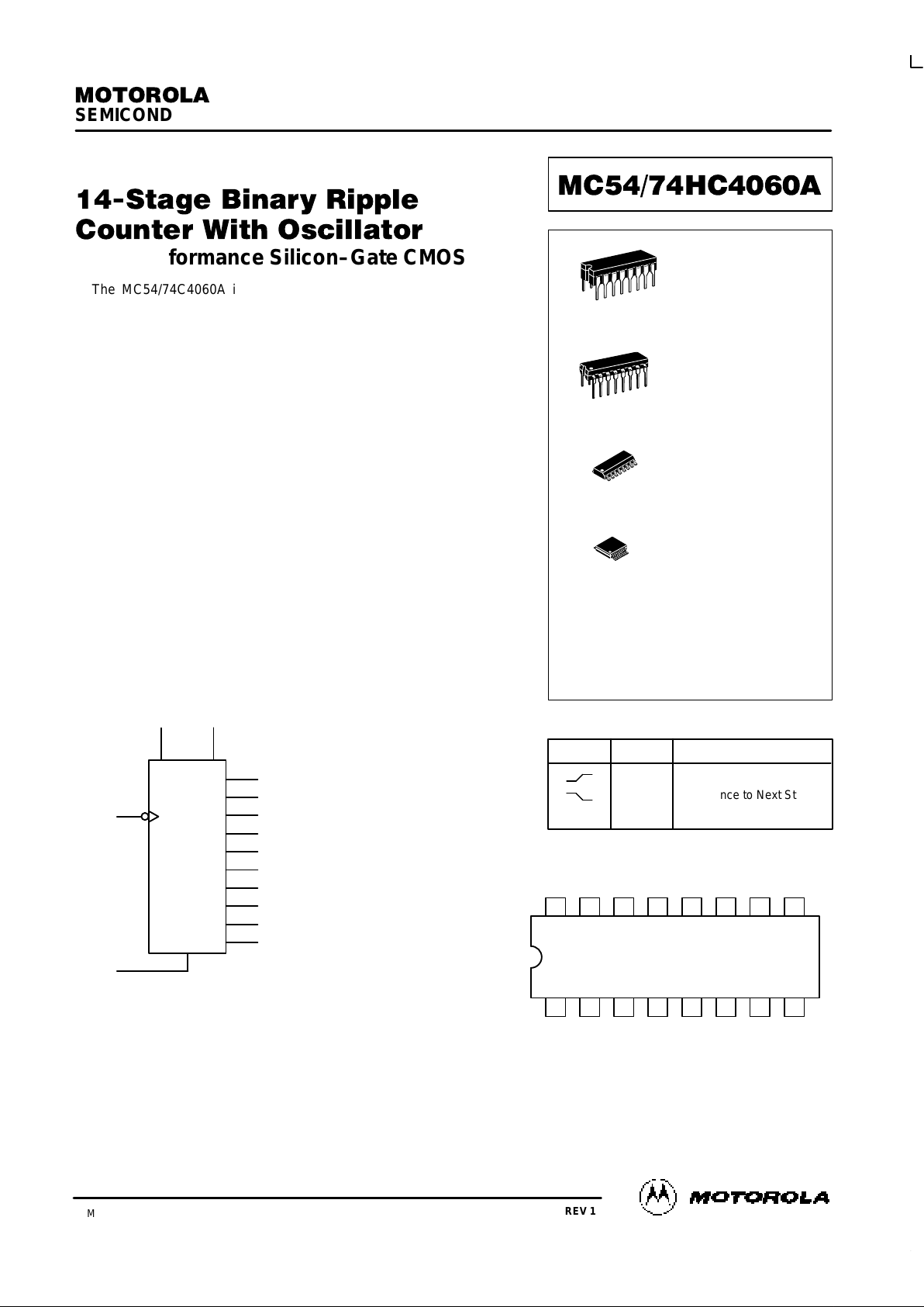
! #
"! ! !
High–Performance Silicon–Gate CMOS
The MC54/74C4060A is identical in pinout to the standard CMOS
MC14060B. The device inputs are compatible with standard CMOS outputs; with pullup resistors, they are compatible with LSTTL outputs.
This device consists of 14 master–slave flip–flops and an oscillator
with a frequency that is controlled either by a crystal or by an RC circuit
connected externally. The output of each flip–flop feeds the next and the
frequency at each output is half of that of the preceding one. The state of
the counter advances on the negative–going edge of the Osc In. The
active–high Reset is asynchronous and disables the oscillator to allow
very low power consumption during stand–by operation.
State changes of the Q outputs do not occur simultaneously because
of internal ripple delays. Therefore, decoded output signals are subject to
decoding spikes and may have to be gated with Osc Out 2 of the
HC4060A.
• Output Drive Capability: 10 LSTTL Loads
• Outputs Directly Interface to CMOS, NMOS, and TTL
• Operating Voltage Range: 2 to 6 V
• Low Input Current: 1 µA
• High Noise Immunity Characteristic of CMOS Devices
• In Compliance With JEDEC Standard No. 7A Requirements
• Chip Complexity: 390 FETs or 97.5 Equivalent Gates
LOGIC DIAGRAM
Q4
7
Q5
5
Q6
4
Q7
6
Q8
14
Q9
13
Q10
15
Q12
1
Q13
2
Q14
3
Osc In
11
Reset
12
Pin 16 = V
CC
Pin 8 = GND
Osc Out 1 Osc Out 2
910
1516 14 13 12 11 10
21 3 4 5 6 7
V
CC
9
8
Q10 Q8 Q9 Reset Osc In
Osc
Out 1
Osc
Out 2
Q12 Q13 Q14 Q6 Q5 Q7 Q4
GND
Pinout: 16–Lead Plastic Package (Top View)
FUNCTION TABLE
Clock Reset Output State
X
L
L
H
No Charge
Advance to Next State
All Outputs Are Low
D SUFFIX
SOIC PACKAGE
CASE 751B–05
N SUFFIX
PLASTIC PACKAGE
CASE 648–08
1
16
1
16
J SUFFIX
CERAMIC PACKAGE
CASE 620–10
1
16
ORDERING INFORMATION
MC54HCXXXXAJ
MC74HCXXXXAN
MC74HCXXXXAD
MC74HCXXXXADT
Ceramic
Plastic
SOIC
TSSOP
1
16
DT SUFFIX
TSSOP PACKAGE
CASE 748C–03
Page 2
MC54/74HC4060A
MOTOROLA High–Speed CMOS Logic Data
DL129 — Rev 6
3–2
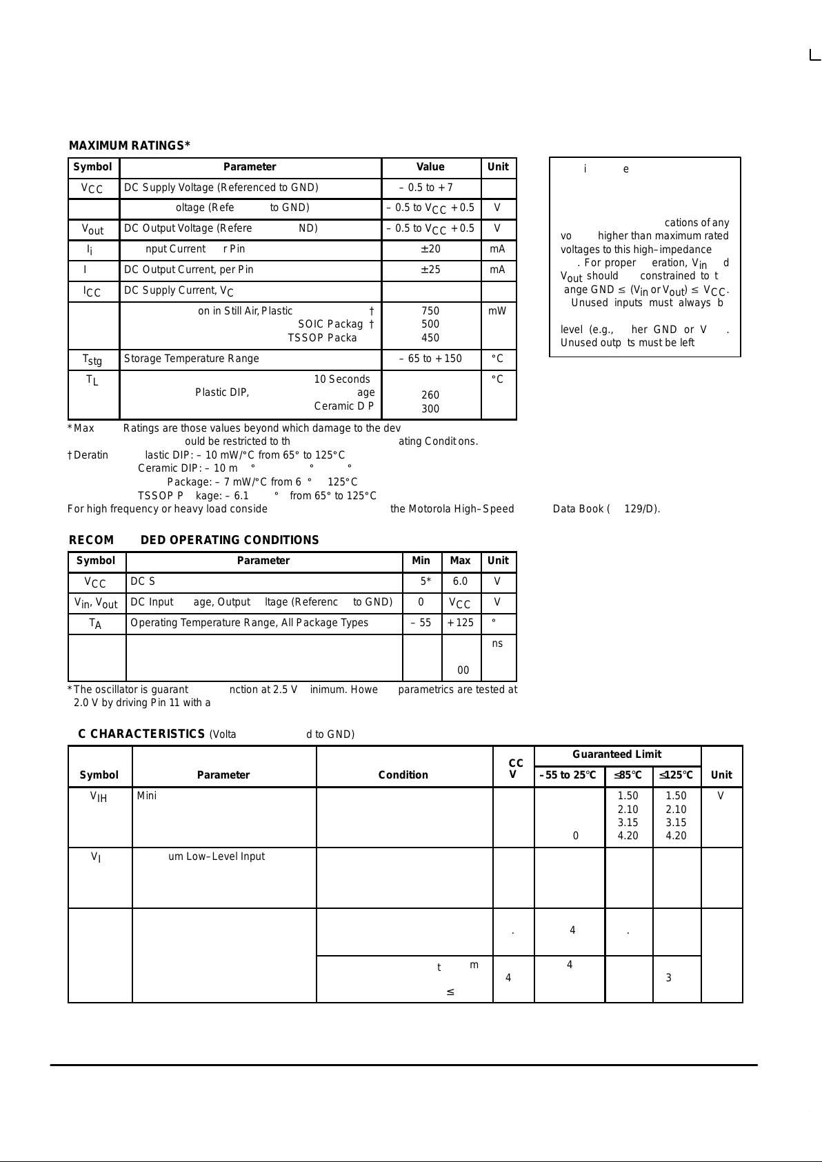
MAXIMUM RATINGS*
Symbol
Parameter
Value
Unit
V
CC
DC Supply Voltage (Referenced to GND)
– 0.5 to + 7.0
V
V
in
DC Input Voltage (Referenced to GND)
– 0.5 to VCC + 0.5
V
V
out
DC Output Voltage (Referenced to GND)
– 0.5 to VCC + 0.5
V
I
in
DC Input Current, per Pin
± 20
mA
I
out
DC Output Current, per Pin
± 25
mA
I
CC
DC Supply Current, VCC and GND Pins
± 50
mA
P
D
Power Dissipation in Still Air,Plastic or Ceramic DIP†
SOIC Package†
TSSOP Package†
750
500
450
mW
T
stg
Storage Temperature Range
– 65 to + 150
_
C
T
L
Lead Temperature, 1 mm from Case for 10 Seconds
Plastic DIP, SOIC or TSSOP Package
Ceramic DIP
260
300
_
C
*Maximum Ratings are those values beyond which damage to the device may occur.
Functional operation should be restricted to the Recommended Operating Conditions.
†Derating — Plastic DIP: – 10 mW/_C from 65_ to 125_C
Ceramic DIP: – 10 mW/_C from 100_ to 125_C
SOIC Package: – 7 mW/_C from 65_ to 125_C
TSSOP Package: – 6.1 mW/_C from 65_ to 125_C
For high frequency or heavy load considerations, see Chapter 2 of the Motorola High–Speed CMOS Data Book (DL129/D).
RECOMMENDED OPERATING CONDITIONS
Symbol
Parameter
Min
Max
Unit
V
CC
DC Supply Voltage (Referenced to GND)
2.5*
6.0
V
Vin, V
out
DC Input Voltage, Output Voltage (Referenced to GND)
0
V
CC
V
T
A
Operating Temperature Range, All Package Types
– 55
+ 125
_
C
tr, t
f
Input Rise/Fall Time VCC = 2.0 V
(Figure 1) VCC = 4.5 V
VCC = 6.0 V
0
0
0
1000
500
400
ns
*The oscillator is guaranteed to function at 2.5 V minimum. However, parametrics are tested at
2.0 V by driving Pin 11 with an external clock source.
DC CHARACTERISTICS (Voltages Referenced to GND)
V
Guaranteed Limit
Symbol
Parameter
Condition
V
CC
V
–55 to 25°C ≤85°C ≤125°C
Unit
V
IH
Minimum High–Level Input Voltage V
out
= 0.1V or VCC –0.1V
|I
out
| ≤ 20µA
2.0
3.0
4.5
6.0
1.50
2.10
3.15
4.20
1.50
2.10
3.15
4.20
1.50
2.10
3.15
4.20
V
V
IL
Maximum Low–Level Input Voltage V
out
= 0.1V or VCC – 0.1V
|I
out
| ≤ 20µA
2.0
3.0
4.5
6.0
0.50
0.90
1.35
1.80
0.50
0.90
1.35
1.80
0.50
0.90
1.35
1.80
V
V
OH
Minimum High–Level Output
Voltage (Q4–Q10, Q12–Q14)
Vin = VIH or V
IL
|I
out
| ≤ 20µA
2.0
4.5
6.0
1.9
4.4
5.9
1.9
4.4
5.9
1.9
4.4
5.9
V
Vin =VIH or V
IL
|I
out
| ≤ 2.4mA
|I
out
| ≤ 4.0mA
|I
out
| ≤ 5.2mA
3.0
4.5
6.0
2.48
3.98
5.48
2.34
3.84
5.34
2.20
3.70
5.20
This device contains protection
circuitry to guard against damage
due to high static voltages or electric
fields. However, precautions must
be taken to avoid applications of any
voltage higher than maximum rated
voltages to this high–impedance circuit. For proper operation, Vin and
V
out
should be constrained to the
range GND v (Vin or V
out
) v VCC.
Unused inputs must always be
tied to an appropriate logic voltage
level (e.g., either GND or VCC).
Unused outputs must be left open.
Page 3
MC54/74HC4060A
High–Speed CMOS Logic Data
DL129 — Rev 6
3–3 MOTOROLA
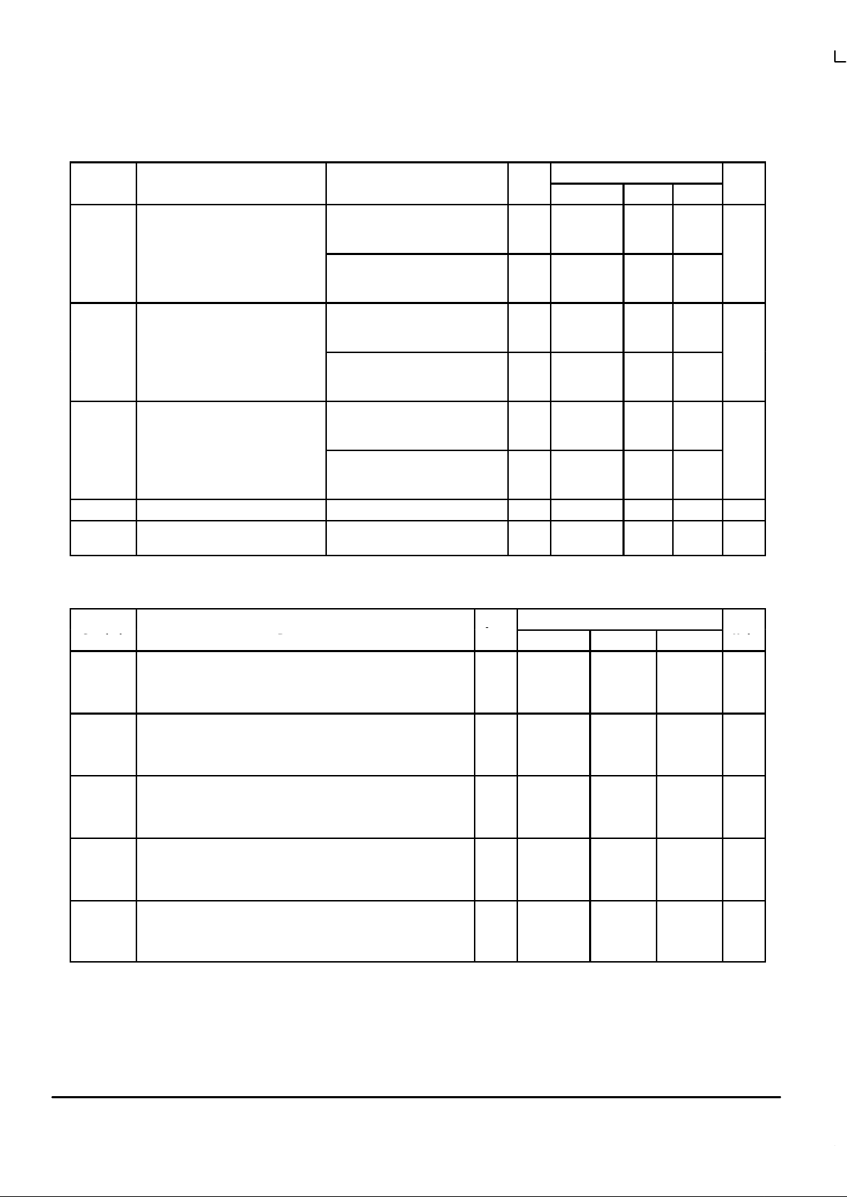
DC CHARACTERISTICS (Voltages Referenced to GND)
Symbol Unit
Guaranteed Limit
V
CC
V
ConditionParameter
Symbol Unit≤125°C≤85°C–55 to 25°C
V
CC
V
ConditionParameter
V
OL
Maximum Low–Level Output
Voltage (Q4–Q10, Q12–Q14)
Vin = VIH or V
IL
|I
out
| ≤ 20µA
2.0
4.5
6.0
0.1
0.1
0.1
0.1
0.1
0.1
0.1
0.1
0.1
V
Vin = VIH or V
IL
|I
out
| ≤ 2.4mA
|I
out
| ≤ 4.0mA
|I
out
| ≤ 5.2mA
3.0
4.5
6.0
0.26
0.26
0.26
0.33
0.33
0.33
0.40
0.40
0.40
V
OH
Minimum High–Level Output
Voltage (Osc Out 1, Osc Out 2)
Vin = VCC or GND
|I
out
| ≤ 20µA
2.0
4.5
6.0
1.9
4.4
5.9
1.9
4.4
5.9
1.9
4.4
5.9
V
Vin =VCC or GND |I
out
| ≤ 0.7mA
|I
out
| ≤ 1.0mA
|I
out
| ≤ 1.3mA
3.0
4.5
6.0
2.48
3.98
5.48
2.34
3.84
5.34
2.20
3.70
5.20
V
OL
Maximum Low–Level Output
Voltage (Osc Out 1, Osc Out 2)
Vin = VCC or GND
|I
out
| ≤ 20µA
2.0
4.5
6.0
0.1
0.1
0.1
0.1
0.1
0.1
0.1
0.1
0.1
V
Vin =VCC or GND |I
out
| ≤ 0.7mA
|I
out
| ≤ 1.0mA
|I
out
| ≤ 1.3mA
3.0
4.5
6.0
0.26
0.26
0.26
0.33
0.33
0.33
0.40
0.40
0.40
I
in
Maximum Input Leakage Current Vin = VCC or GND 6.0 ±0.1 ±1.0 ±1.0 µA
I
CC
Maximum Quiescent Supply
Current (per Package)
Vin = VCC or GND
I
out
= 0µA
6.0 4 40 160 µA
NOTE: Information on typical parametric values can be found in Chapter 2 of the Motorola High–Speed CMOS Data Book (DL129/D).
AC CHARACTERISTICS (C
L
= 50 pF, Input tr = tf = 6 ns)
V
Guaranteed Limit
Symbol
Parameter
V
CC
V
–55 to 25°C ≤85°C ≤125°C
Unit
f
max
Maximum Clock Frequency (50% Duty Cycle)
(Figures 1 and 4)
2.0
3.0
4.5
6.0
6.0
10
30
50
9.0
14
28
45
8.0
12
25
40
MHz
t
PLH
,
t
PHL
Maximum Propagation Delay, Osc In to Q4*
(Figures 1 and 4)
2.0
3.0
4.5
6.0
300
180
60
51
375
200
75
64
450
250
90
75
ns
t
PLH
,
t
PHL
Maximum Propagation Delay, Osc In to Q14*
(Figures 1 and 4)
2.0
3.0
4.5
6.0
500
350
250
200
750
450
275
220
1000
600
300
250
ns
t
PHL
Maximum Propagation Delay, Reset to Any Q
(Figures 2 and 4)
2.0
3.0
4.5
6.0
195
75
39
33
245
100
49
42
300
125
61
53
ns
t
PLH
,
t
PHL
Maximum Propagation Delay, Qn to Qn+1
(Figures 3 and 4)
2.0
3.0
4.5
6.0
75
60
15
13
95
75
19
16
125
95
24
20
ns
Page 4
MC54/74HC4060A
MOTOROLA High–Speed CMOS Logic Data
DL129 — Rev 6
3–4
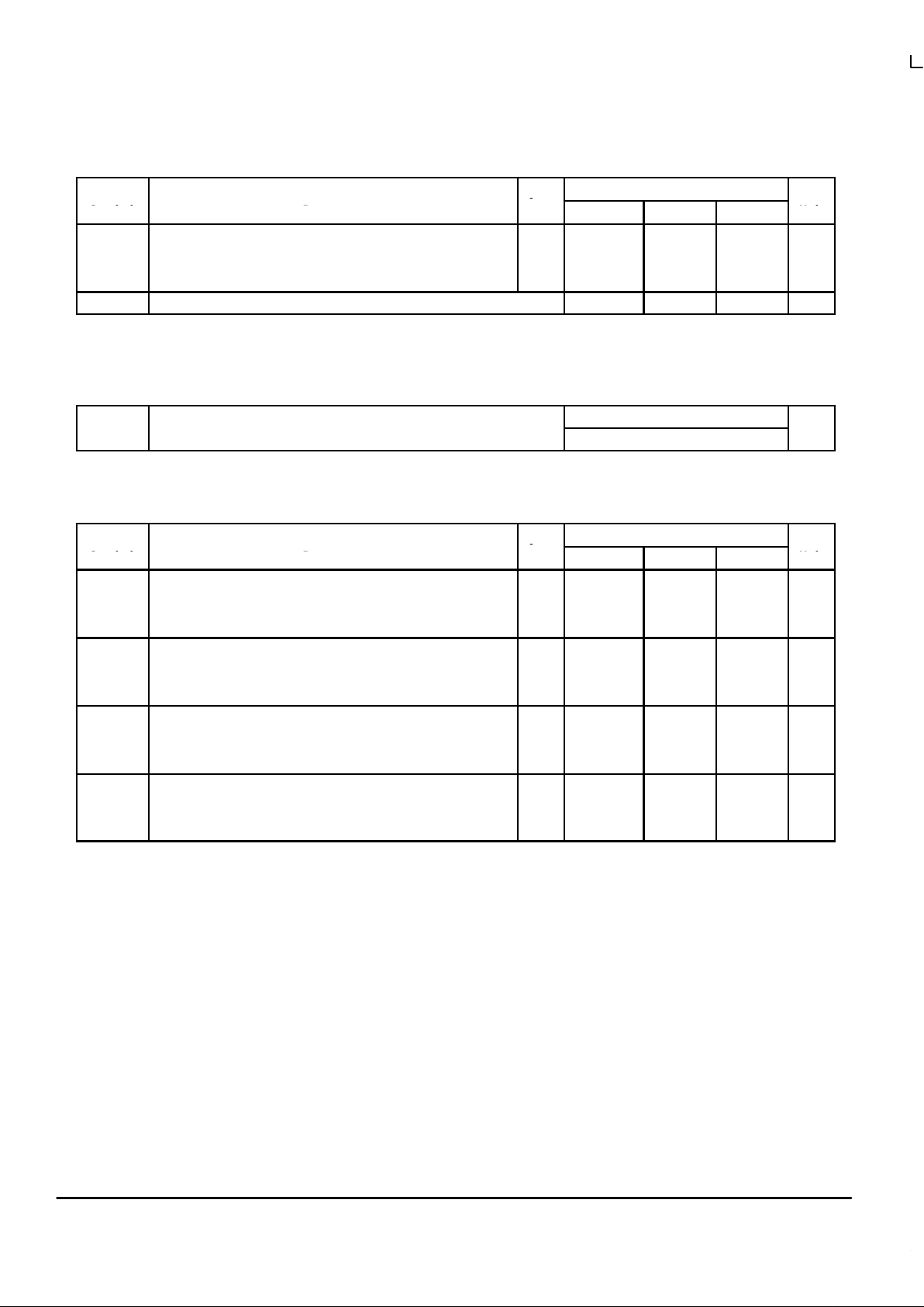
AC CHARACTERISTICS (C
L
= 50 pF, Input tr = tf = 6 ns) – continued
V
Guaranteed Limit
Symbol
Parameter
V
CC
V
–55 to 25°C ≤85°C ≤125°C
Unit
t
TLH
,
t
THL
Maximum Output Transition Time, Any Output
(Figures 1 and 4)
2.0
3.0
4.5
6.0
75
27
15
13
95
32
19
16
110
36
22
19
ns
C
in
Maximum Input Capacitance 10 10 10 pF
NOTE: For propagation delays with loads other than 50 pF, and information on typical parametric values, see Chapter 2 of the Motorola High–
Speed CMOS Data Book (DL129/D).
* For TA = 25°C and CL = 50 pF, typical propagation delay from Clock to other Q outputs may be calculated with the following equations:
VCC = 2.0 V: tP = [93.7 + 59.3 (n–1)] ns VCC = 4.5 V: tP = [30.25 + 14.6 (n–1)] ns
VCC = 3.0 V: tP = [61.5+ 34.4 (n–1)] ns VCC = 6.0 V: tP = [24.4 + 12 (n–1)] ns
Typical @ 25°C, VCC = 5.0 V
C
PD
Power Dissipation Capacitance (Per Package)*
35
pF
*Used to determine the no–load dynamic power consumption: PD = CPD V
CC
2
f + ICC VCC. For load considerations, see Chapter 2 of the
Motorola High–Speed CMOS Data Book (DL129/D).
TIMING REQUIREMENTS (Input t
r
= tf = 6 ns)
V
Guaranteed Limit
Symbol
Parameter
V
CC
V
–55 to 25°C ≤85°C ≤125°C
Unit
t
rec
Minimum Recovery Time, Reset Inactive to Clock
(Figure 2)
2.0
3.0
4.5
6.0
100
75
20
17
125
100
25
21
150
120
30
25
ns
t
w
Minimum Pulse Width, Clock
(Figure 1)
2.0
3.0
4.5
6.0
75
27
15
13
95
32
19
16
110
36
23
19
ns
t
w
Minimum Pulse Width, Reset
(Figure 2)
2.0
3.0
4.5
6.0
75
27
15
13
95
32
19
16
110
36
23
19
ns
tr, t
f
Maximum Input Rise and Fall Times
(Figure 1)
2.0
3.0
4.5
6.0
1000
800
500
400
1000
800
500
400
1000
800
500
400
ns
NOTE: Information on typical parametric values can be found in Chapter 2 of the Motorola High–Speed CMOS Data Book (DL129/D).
Page 5

MC54/74HC4060A
High–Speed CMOS Logic Data
DL129 — Rev 6
3–5 MOTOROLA
PIN DESCRIPTIONS
INPUTS
Osc In (Pin 11)
Negative–edge triggering clock input. A high–to–low transition on this input advances the state of the counter. Osc In
may be driven by an external clock source.
Reset (Pin 12)
Active–high reset. A high level applied to this input asynchronously resets the counter to its zero state (forcing all Q outputs low) and disables the oscillator.
OUTPUTS
Q4—Q10, Q12–Q14 (Pins 7, 5, 4, 6, 13, 15, 1, 2, 3)
Active–high outputs. Each Qn output divides the Clock
input frequency by 2N. The user should note the Q1, Q2, Q3
and Q11 are not available as outputs.
Osc Out 1, Osc Out 2 (Pins 9, 10)
Oscillator outputs. These pins are used in conjunction with
Osc In and the external components to form an oscillator
(See NO TAG and NO TAG). When Osc In is being driven
with an external clock source, Osc Out 1 and Osc Out 2 must
be left open circuited. With the crystal oscillator configuration
in Figure 6, Osc Out 2 must be left open circuited.
SWITCHING WAVEFORMS
t
w
t
f
Osc In
Q
V
CC
GND
90%
50%
10%
t
r
t
w
90%
50%
10%
t
PHL
1/f
MAX
t
PLH
t
TLH
t
THL
Reset
V
CC
GND
t
PHL
50%
Figure 1. Figure 2.
Q
V
CC
GND
50%
Osc In 50%
t
rec
50%
Qn
V
CC
GND
50%
Qn+1
CL*
*Includes all probe and jig capacitance
TEST
POINT
DEVICE
UNDER
TEST
OUTPUT
Figure 3. Figure 4. Test Circuit
t
PLH
t
PHL
Page 6

MC54/74HC4060A
MOTOROLA High–Speed CMOS Logic Data
DL129 — Rev 6
3–6
Figure 5. Expanded Logic Diagram
C
C
R
Osc Out 2
9
Q
Q
C
C
R
Q
Q
C
CQQ
C
CQQ
C
CQQ
C
C
Q
Q4
7
Q5
5
Q12
1
Q13
2
Q14
3
Q6 = Pin 4
Q7 = Pin 6
Q8 = Pin 14
Q9 = Pin 13
Q10 = Pin 15
VCC = Pin 16
GND = Pin 8
Osc Out 1
10
Osc In
11
Reset
12
Figure 6. Oscillator Circuit Using RC Configuration
Reset
12
Osc In 11 Osc Out 1 10 Osc Out 2 9
R
tc
C
tc
R
S
For 2.0V
≤
VCC ≤ 6.0V
10Rtc > RS > 2R
tc
400Hz
≤
f ≤ 400Khz:
f
[
1
3 RtcC
tc
(f in Hz, Rtcin ohms, Ctcin farads)
The formula may vary for other frequencies.
Figure 7. Pierce Crystal Oscillator Circuit
Reset
12
Osc In 11 Osc Out 1 10 9 Osc Out 2
R
f
C1 C2
R1
Page 7

MC54/74HC4060A
High–Speed CMOS Logic Data
DL129 — Rev 6
3–7 MOTOROLA
TABLE 1. CRYSTAL OSCILLATOR AMPLIFIER SPECIFICATIONS (T
A
= 25°C; Input = Pin 11, Output = Pin 10)
Type
Positive Reactance (Pierce)
Input Resistance, R
in
60MΩ Minimum
Output Impedance, Z
out
(4.5V Supply) 200Ω (See Text)
Input Capacitance, C
in
5pF Typical
Output Capacitance, C
out
7pF Typical
Series Capacitance, C
a
5pF Typical
Open Loop Voltage Gain with Output at Full Swing, α 3Vdc Supply
4Vdc Supply
5Vdc Supply
6Vdc Supply
5.0 Expected Minimum
4.0 Expected Minimum
3.3 Expected Minimum
3.1 Expected Minimum
PIERCE CRYSTAL OSCILLATOR DESIGN
Figure 8. Equivalent Crystal Networks
R
S
LSC
S
Re Xe 212121
C
O
Value are supplied by crystal manufacturer (parallel resonant crystal).
Figure 9. Series Equivalent Crystal Load Figure 10. Parasitic Capacitances of the Amplifier
Z
load
–jX
Co
–jX
C2
R
–jX
C
–jX
Cs
jX
Ls
R
S
R
load
X
load
NOTE: C = C1 + Cin and R = R1 + R
out
. Co is considered as part of
the load. Ca and Rf typically have minimal effect below 2MHz.
C
in
C
out
C
a
Values are listed in Table 1.
Page 8

MC54/74HC4060A
MOTOROLA High–Speed CMOS Logic Data
DL129 — Rev 6
3–8
DESIGN PROCEDURES
The following procedure applies for oscillators operating below 2MHz where Z is a resistor R1. Above 2MHz, additional
impedance elements should be considered: C
out
and Ca of the amp, feedback resistor Rf, and amplifier phase shift error from
180°C.
Step 1: Calculate the equivalent series circuit of the crystal at the frequency of oscillation.
Z
e
+
*
jX
C
o
(Rs)
jX
L
s
*
jX
C
s
)
*
jX
C
o
)
Rs)
jX
L
s
*
jX
C
s
+
Re)
jX
e
Reactance jXe should be positive, indicating that the crystal is operating as an inductive reactance at the oscillation frequency.
The maximum Rs for the crystal should be used in the equation.
Step 2: Determine β, the attenuation, of the feedback network. For a closed-loop gain of 2,Aνβ = 2,β = 2/Aν where Aν is the gain
of the HC4060A amplifier.
Step 3: Determine the manufacturer’s loading capacitance. For example: A manufacturer may specify an external load capaci-
tance of 32pF at the required frequency.
Step 4: Determine the required Q of the system, and calculate R
load
, For example, a manufacturer specifies a crystal Q of
100,000. In-circuit Q is arbitrarily set at 20% below crystal Q or 80,000. Then R
load
= (2πfoLS/Q) – Rs where Ls and Rs are crystal
parameters.
Step 5: Simultaneously solve, using a computer,
b
+
XC@
X
C2
R@Re)
XC2(Xe*
XC)
( Eq 1 )(with feedback phase shift = 180°)
Xe+
XC2)
XC)
ReX
C2
R
+
X
C
load
( Eq 2 )(where the loading capacitor is an external load, not including Co)
R
load
+
RX
C
o
XC2[(XC)
XC2)(XC)
X
C
o
)*XC(XC)
X
C
o
)
XC2)]
X
2
C2(XC
)
X
C
o
)2)
R2(XC)
X
C
o
)
XC2)
2
( Eq 3 )
Here R = R
out
+ R1. R
out
is amp output resistance, R1 is Z. The C corresponding to XC is given by C = C1 + Cin.
Alternately, pick a value for R1 (i.e, let R1 = RS). Solve Equations 1 and 2 for C1 and C2. Use Equation 3 and the fact that Q =
2πfoLs/(Rs + R
load
) to find in-circuit Q. If Q is not satisfactory pick another value for R1 and repeat the procedure.
CHOOSING R1
Power is dissipated in the effective series resistance of the
crystal. The drive level specified by the crystal manufacturer
is the maximum stress that a crystal can withstand without
damage or excessive shift in frequency. R1 limits the drive
level.
To verify that the maximum dc supply voltage does not
overdrive the crystal, monitor the output frequency as a function of voltage at Osc Out 2 (Pin 9). The frequency should
increase very slightly as the dc supply voltage is increased.
An overdriven crystal will decrease in frequency or become
unstable with an increase in supply voltage. The operating
supply voltage must be reduced or R1 must be increased in
value if the overdriven condition exists. The user should note
that the oscillator start-up time is proportional to the value of
R1.
SELECTING R
f
The feedback resistor, Rf, typically ranges up to 20MΩ. R
f
determines the gain and bandwidth of the amplifier. Proper
bandwidth insures oscillation at the correct frequency plus
roll-off to minimize gain at undesirable frequencies, such as
the first overtone. Rf must be large enough so as to not affect
the phase of the feedback network in an appreciable manner.
ACKNOWLEDGEMENTS AND RECOMMENDED
REFERENCES
The following publications were used in preparing this data
sheet and are hereby acknowledged and recommended for
reading:
Technical Note TN-24, Statek Corp.
Technical Note TN-7, Statek Corp.
D. Babin, “Designing Crystal Oscillators”, Machine Design,
March 7, 1985.
D. Babin, “ Guidelines for C rystal Oscillator D esign”,
Machine Design, April 25, 1985.
ALSO RECOMMENDED FOR READING:
E. Hafner, “The Piezoelectric Crystal Unit-Definitions and
Method of Measurement”, Proc. IEEE, Vol. 57, No. 2, Feb.,
1969.
D. Kemper, L. Rosine, “Quartz Crystals for Frequency
Control”, Electro-Technology, June, 1969.
P. J. Ottowitz, “A Guide to Crystal Selection”, Electronic
Design, May, 1966.
Page 9

MC54/74HC4060A
High–Speed CMOS Logic Data
DL129 — Rev 6
3–9 MOTOROLA
Clock
Reset
Q4
1 2 4 8 16 32 64 128 256 512 1024 2048 4096 8192 16384
Q5
Q6
Q7
Q8
Q9
Q10
Q12
Q13
Q14
Figure 11. Timing Diagram
Page 10

MC54/74HC4060A
MOTOROLA High–Speed CMOS Logic Data
DL129 — Rev 6
3–10
OUTLINE DIMENSIONS
J SUFFIX
CERAMIC PACKAGE
CASE 620–10
ISSUE V
N SUFFIX
PLASTIC PACKAGE
CASE 648–08
ISSUE R
19.05
6.10
—
0.39
1.40
0.21
3.18
19.93
7.49
5.08
0.50
1.65
0.38
4.31
0
°
0.51
15
°
1.01
1.27 BSC
2.54 BSC
7.62 BSC
MIN MINMAX MAX
INCHES MILLIMETERS
DIM
0.750
0.240
—
0.015
0.055
0.008
0.125
0.785
0.295
0.200
0.020
0.065
0.015
0.170
0.050 BSC
0.100 BSC
0.300 BSC
A
B
C
D
E
F
G
J
K
L
M
N
0
°
0.020
15
°
0.040
NOTES:
1. DIMENSIONING AND TOLERANCING PER
ANSI Y14.5M, 1982.
2. CONTROLLING DIMENSION: INCH.
3. DIMENSION L TO CENTER OF LEAD WHEN
FORMED PARALLEL.
4. DIM F MAY NARROW TO 0.76 (0.030) WHERE
THE LEAD ENTERS THE CERAMIC BODY.
1 8
916
–A
–
–B
–
C
K
N
G
E
F
D 16 PL
–T
–
SEATING
PLANE
M
L
J 16 PL
0.25 (0.010) T A
M
S
0.25 (0.010) T B
M
S
MIN MINMAX MAX
INCHES MILLIMETERS
DIM
A
B
C
D
F
G
H
J
K
L
M
S
18.80
6.35
3.69
0.39
1.02
0.21
2.80
7.50
0
°
0.51
19.55
6.85
4.44
0.53
1.77
0.38
3.30
7.74
10
°
1.01
0.740
0.250
0.145
0.015
0.040
0.008
0.110
0.295
0
°
0.020
0.770
0.270
0.175
0.021
0.070
0.015
0.130
0.305
10
°
0.040
NOTES:
1. DIMENSIONING AND TOLERANCING PER ANSI
Y14.5M, 1982.
2. CONTROLLING DIMENSION: INCH.
3. DIMENSION L TO CENTER OF LEADS WHEN
FORMED PARALLEL.
4. DIMENSION B DOES NOT INCLUDE MOLD FLASH.
5. ROUNDED CORNERS OPTIONAL.
2.54 BSC
1.27 BSC
0.100 BSC
0.050 BSC
–A
–
B
1 8
916
F
H
G
D
16 PL
S
C
–T
–
SEATING
PLANE
K
J
M
L
T A0.25 (0.010)
M M
0.25 (0.010) T B A
M
S S
MIN MINMAX MAX
MILLIMETERS INCHES
DIM
A
B
C
D
F
G
J
K
M
P
R
9.80
3.80
1.35
0.35
0.40
0.19
0.10
0
°
5.80
0.25
10.00
4.00
1.75
0.49
1.25
0.25
0.25
7
°
6.20
0.50
0.386
0.150
0.054
0.014
0.016
0.008
0.004
0
°
0.229
0.010
0.393
0.157
0.068
0.019
0.049
0.009
0.009
7
°
0.244
0.019
1.27 BSC 0.050 BSC
NOTES:
1. DIMENSIONING AND TOLERANCING PER ANSI
Y14.5M, 1982.
2. CONTROLLING DIMENSION: MILLIMETER.
3. DIMENSIONS A AND B DO NOT INCLUDE
MOLD PROTRUSION.
4. MAXIMUM MOLD PROTRUSION 0.15 (0.006)
PER SIDE.
5. DIMENSION D DOES NOT INCLUDE DAMBAR
PROTRUSION. ALLOWABLE DAMBAR
PROTRUSION SHALL BE 0.127 (0.005) TOTAL
IN EXCESS OF THE D DIMENSION AT
MAXIMUM MATERIAL CONDITION.
1
8
916
–A
–
–B
–
D 16 PL
K
C
G
–T
–
SEATING
PLANE
R X 45°
M
J
F
P 8 PL
0.25 (0.010) B
M M
D SUFFIX
PLASTIC SOIC PACKAGE
CASE 751B–05
ISSUE J
Page 11

MC54/74HC4060A
High–Speed CMOS Logic Data
DL129 — Rev 6
3–11 MOTOROLA
OUTLINE DIMENSIONS
DT SUFFIX
TSSOP PACKAGE
CASE 948C–03
ISSUE B
A
B
PIN 1
IDENTIFICATION
L
1 8
916
D
C
SEATING
G
H
F
M
DIMAMIN MAX MIN MAX
INCHES
––– 5.10 ––– 0.200
MILLIMETERS
B 4.30 4.50 0.169 0.177
C ––– 1.20 ––– 0047
D 0.05 0.25 0.002 0.010
F 0.45 0.55 0.018 0.022
G 0.65 BSC 0.026 BSC
H 0.22 0.23 0.009 0.010
J 0.09 0.24 0.004 0.009
K 0.16 0.32 0.006 0.013
L 6.30 6.50 0.248 0.256
M 0 10 0 10
NOTES:
1. DIMENSIONING AND TOLERANCING PER ANSI
Y14.5M, 1982.
2. CONTROLLING DIMENSION: MILLIMETER.
3. DIMENSION A DOES NOT INCLUDE MOLD FLASH,
PROTRUSIONS OR GATE BURRS. MOLD FLASH
OR GATE BURRS SHALL NOT EXCEED 0.15 (0.006)
PER SIDE.
4. DIMENSION B DOES NOT INCLUDE INTERLEAD
FLASH OR PROTRUSION. INTERLEAD FLASH OR
PROTRUSION SHALL NOT EXCEED 0.25 (0.010)
PER SIDE.
5. DIMENSION K DOES NOT INCLUDE DAMBAR
PROTRUSION. ALLOWABLE DAMBAR
PROTRUSION SHALL BE 0.08 (0.003) TOTAL
EXCESS OF THE K DIMENSION AT MAXIMUM
MATERIAL CONDITION.
6. TERMINAL NUMBERS ARE SHOWN FOR
REFERENCE ONLY.
7. DIMENSIONS A AND B ARE TO BE DETERMINED
AT DATUM PLANE –U–.
° ° ° °
J1 0.09 0.18 0.004 0.007
K1 0.16 0.26 0.006 0.010
K
K1
J
J1
SECTION A–A
A
A
16x REFK
0.100 (0.004)
M
0.200 (0.008)MT
PLANE
–P–
–T–
–U–
How to reach us:
USA/EUROPE: Motorola Literature Distribution; JAPAN: Nippon Motorola Ltd.; Tatsumi–SPD–JLDC, Toshikatsu Otsuki,
P.O. Box 20912; Phoenix, Arizona 85036. 1–800–441–2447 6F Seibu–Butsuryu–Center, 3–14–2 Tatsumi Koto–Ku, Tokyo 135, Japan. 03–3521–8315
MFAX: RMFAX0@email.sps.mot.com –TOUCHTONE (602) 244–6609 HONG KONG: Motorola Semiconductors H.K. Ltd.; 8B Tai Ping Industrial Park,
INTERNET: http://Design–NET.com 51 Ting Kok Road, Tai Po, N.T., Hong Kong. 852–26629298
Motorola reserves the right to make changes without further notice to any products herein. Motorola makes no warranty , representation or guarantee regarding
the suitability of its products for any particular purpose, nor does Motorola assume any liability arising out of the application or use of any product or circuit,
and specifically disclaims any and all liability, including without limitation consequential or incidental damages. “T ypical” parameters can and do vary in different
applications. All operating parameters, including “T ypicals” must be validated for each customer application by customer’s technical experts. Motorola does
not convey any license under its patent rights nor the rights of others. Motorola products are not designed, intended, or authorized for use as components in
systems intended for surgical implant into the body, or other applications intended to support or sustain life, or for any other application in which the failure of
the Motorola product could create a situation where personal injury or death may occur. Should Buyer purchase or use Motorola products for any such
unintended or unauthorized application, Buyer shall indemnify and hold Motorola and its officers, employees, subsidiaries, affiliates, and distributors harmless
against all claims, costs, damages, and expenses, and reasonable attorney fees arising out of, directly or indirectly, any claim of personal injury or death
associated with such unintended or unauthorized use, even if such claim alleges that Motorola was negligent regarding the design or manufacture of the part.
Motorola and are registered trademarks of Motorola, Inc. Motorola, Inc. is an Equal Opportunity/Affirmative Action Employer.
MC54/74HC4060A/D
*MC54/74HC4060A/D*
◊
CODELINE
 Loading...