

Page 1

http://onsemi.com
This document,
MC74HC4051/D
has been canceled and
replaced by
MC74HC4051A/D
LAN was sent 9/28/01
Page 2
MC54/74HC4051 MC74HC4052 MC54/74HC4053
Analog Multiplexers/
Demultiplexers
High–Performance Silicon–Gate CMOS
The MC54/74HC4051, MC74HC4052 and MC54/74HC4053 utilize silicon–gate CMOS technology to achieve fast propagation delays, low ON
resistances, and low OFF leakage currents. These analog multiplexers/
demultiplexers control analog voltages that may vary across the complete
power supply range (from V
The HC4051, HC4052 and HC4053 are identical in pinout to the
metal–gate MC14051B, MC14052B and MC14053B. The Channel–Select
inputs determine which one of the Analog Inputs/Outputs is to be connected,
by means of an analog switch, to the Common Output/Input. When the
Enable pin is HIGH, all analog switches are turned off.
The Channel–Select and Enable inputs are compatible with standard
CMOS outputs; with pullup resistors they are compatible with LSTTL
outputs.
These devices have been designed so that the ON resistance (R
more linear over input voltage than R
switches.
For multiplexers/demultiplexers with channel–select latches, see
HC4351, HC4352 and HC4353.
• Fast Switching and Propagation Speeds
• Low Crosstalk Between Switches
• Diode Protection on All Inputs/Outputs
• Analog Power Supply Range (V
• Digital (Control) Power Supply Range (V
• Improved Linearity and Lower ON Resistance Than Metal–Gate
Counterparts
• Low Noise
• In Compliance With the Requirements of JEDEC Standard No. 7A
• Chip Complexity: HC4051 — 184 FETs or 46 Equivalent Gates
HC4052 — 168 FETs or 42 Equivalent Gates
HC4053 — 156 FETs or 39 Equivalent Gates
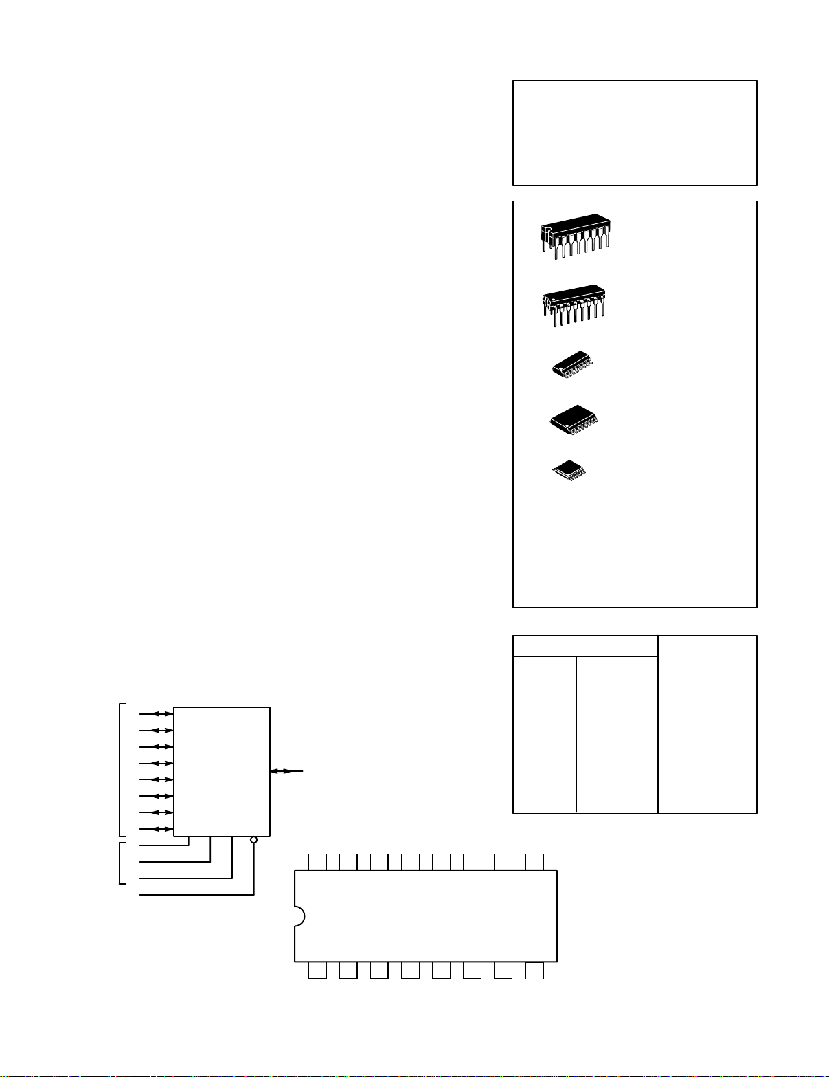
LOGIC DIAGRAM
MC54/74HC4051
Single–Pole, 8–Position Plus Common Off
13
X0
14
X1
15
ANALOG
INPUTS/
OUTPUTS
CHANNEL
SELECT
INPUTS
X2
X3
X4
X5
X6
X7
ENABLE
12
1
5
2
4
11
A
10
B
9
C
6
PIN 16 = V
PIN 7 = V
PIN 8 = GND
MULTIPLEXER/
DEMULTIPLEXER
CC
EE
to VEE).
CC
of metal–gate CMOS analog
on
– VEE) = 2.0 to 12.0 V
CC
– GND) = 2.0 to 6.0 V
CC
3
COMMON
X
OUTPUT/
INPUT
Pinout: MC54/74HC4051 (Top View)
V
X2 X1 X0 X3 A B C
CC
1516 14 13 12 11 10
on
) is
MC54/74HC4051
MC74HC4052
MC54/74HC4053
J SUFFIX
16
1
16
1
16
1
16
1
16
1
ORDERING INFORMATION
MC54HCXXXXJ
MC74HCXXXXN
MC74HCXXXXD
MC74HCXXXXDW
MC74HCXXXXDT
FUNCTION TABLE – MC54/74HC4051
Control Inputs
Enable
L
L
L
L
L
L
L
L
H
9
CBA
L
L
L
L
H
H
H
H
X
CERAMIC PACKAGE
CASE 620–10
PLASTIC PACKAGE
CASE 648–08
SOIC PACKAGE
CASE 751B–05
DW SUFFIX
SOIC PACKAGE
CASE 751G–02
DT SUFFIX
TSSOP PACKAGE
CASE 948F–01
Select
L
L
L
H
H
L
H
H
L
L
L
H
H
L
H
H
X
X
N SUFFIX
D SUFFIX
Ceramic
Plastic
SOIC
SOIC Wide
TSSOP
ON Channels
X0
X1
X2
X3
X4
X5
X6
X7
NONE
X = Don’t Care
21 34567
X4 X6 X X7 X5 Enable V
8
GND
EE
Page 3
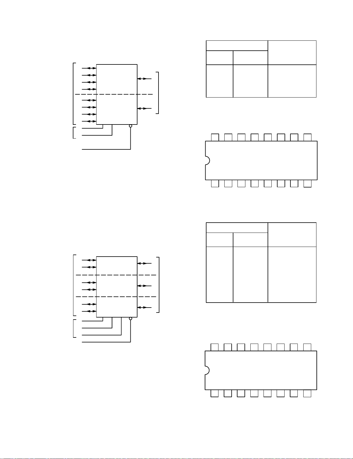
Double–Pole, 4–Position Plus Common Off
INPUTS/OUTPUTS
CHANNELSELECT
ANALOG
INPUTS
X0
X1
X2
X3
Y0
Y1
Y2
Y3
ENABLE
LOGIC DIAGRAM
MC74HC4052
12
14
15
11
1
5
2
4
10
A
9
B
6
X SWITCH
Y SWITCH
13
X
3
Y
PIN 16 = V
PIN 7 = V
EE
PIN 8 = GND
MC54/74HC4051 MC74HC4052 MC54/74HC4053
FUNCTION TABLE – MC74HC4052
Control Inputs
Select
BA
L
L
L
H
H
H
X
L
H
X
ON Channels
Y0
Y1
Y2
Y3
NONE
X2 X1 X X0 X3 A B
1516 14 13 12 11 10
COMMON
OUTPUTS/INPUTS
CC
Enable
L
L
L
L
H
X = Don’t Care
Pinout: MC74HC4052 (Top View)
V
CC
X0
X1
X2
X3
9
LOGIC DIAGRAM
MC54/74HC4053
Triple Single–Pole, Double–Position Plus Common Off
12
X0
INPUTS/OUTPUTS
CHANNELSELECT
ANALOG
INPUTS
X1
Y0
Y1
Z0
Z1
ENABLE
13
2
1
5
3
11
A
10
B
9
C
6
X SWITCH
Y SWITCH
Z SWITCH
NOTE: This device allows independent control of each switch.
Channel–Select Input A controls the X–Switch, Input B controls
the Y–Switch and Input C controls the Z–Switch
14
X
15
Y
4
Z
PIN 16 = V
PIN 7 = V
EE
PIN 8 = GND
CC
COMMON
OUTPUTS/INPUTS
21 34567
Y0 Y2 Y Y3 Y1 Enable V
FUNCTION TABLE – MC54/74HC4053
Control Inputs
Select
L
H
L
H
L
H
L
H
X
ON Channels
Z0
Y0
Z0
Y0
Z0
Y1
Z0
Y1
Z1
Y0
Z1
Y0
Z1
Y1
Z1
Y1
NONE
Enable
L
L
L
L
L
L
L
L
H
CBA
L
L
L
L
L
H
L
H
H
L
H
L
H
H
H
H
X
X
X = Don’t Care
Pinout: MC54/74HC4053 (Top View)
V
Y X X1 X0 A B C
CC
1516 14 13 12 11 10
8
GND
EE
X0
X1
X0
X1
X0
X1
X0
X1
9
21 34567
Y1 Y0 Z1 Z Z0 Enable V
8
GND
EE
Page 4
MC54/74HC4051 MC74HC4052 MC54/74HC4053
Î
Î
Î
Î
Î
Î
Î
Î
Î
Î
Î
Î
Î
Î
Î
Î
Î
Î
Î
Î
Î
Î
Î
Î
Î
Î
Î
Î
Î
Î
Î
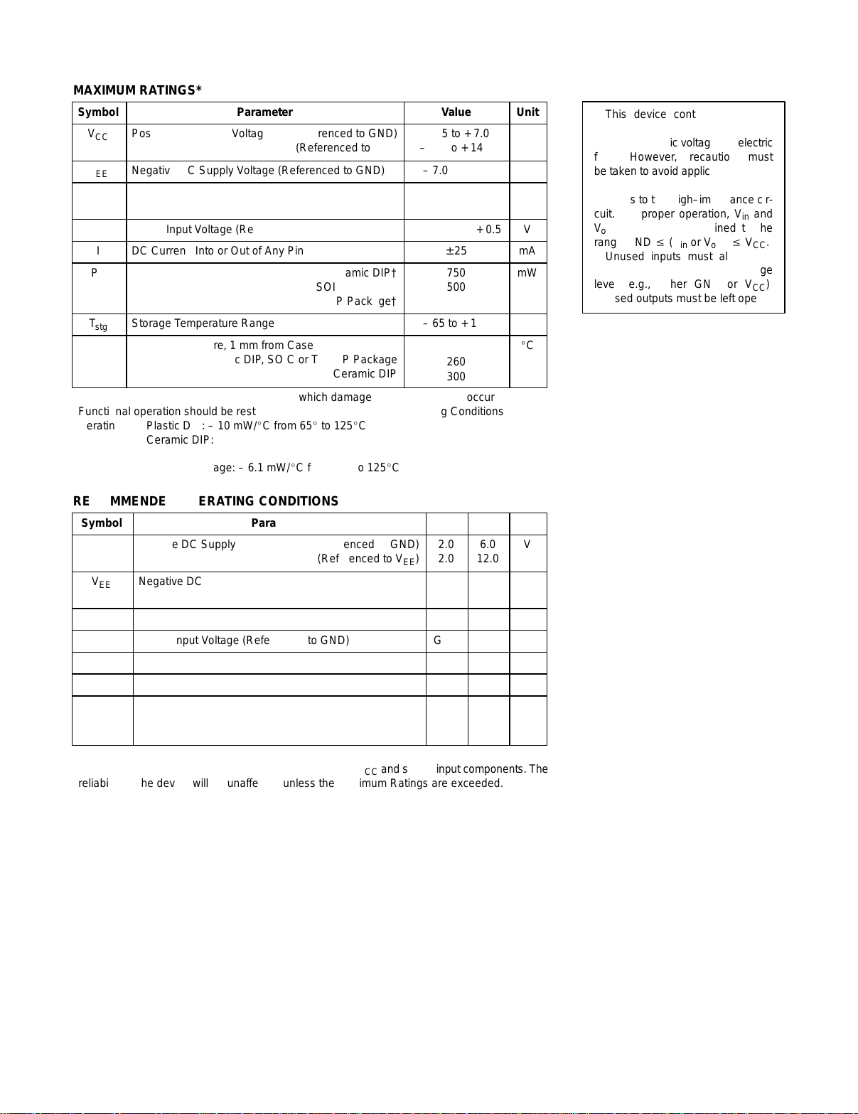
MAXIMUM RATINGS*
Symbol
V
Î
V
Î
Î
T
Î
Positive DC Supply Voltage (Referenced to GND)
CC
ОООООООООООО
Negative DC Supply Voltage (Referenced to GND)
EE
V
Analog Input Voltage
IS
ОООООООООООО
V
Digital Input Voltage (Referenced to GND)
in
I
DC Current, Into or Out of Any Pin
P
Power Dissipation in Still Air,Plastic or Ceramic DIP†
D
ОООООООООООО
Storage Temperature Range
stg
T
Lead Temperature, 1 mm from Case for 10 Seconds
L
ОООООООООООО
*Maximum Ratings are those values beyond which damage to the device may occur.
Functional operation should be restricted to the Recommended Operating Conditions.
†Derating — Plastic DIP: – 10 mW/C from 65 to 125C
Ceramic DIP: – 10 mW/C from 100 to 125C
SOIC Package: – 7 mW/C from 65 to 125C
TSSOP Package: – 6.1 mW/C from 65 to 125C
Parameter
(Referenced to V
EE
SOIC Package†
TSSOP Package†
Plastic DIP, SOIC or TSSOP Package
Ceramic DIP
Value
– 0.5 to + 7.0
– 0.5 to + 14.0
)
ÎÎÎÎ
– 7.0 to + 5.0
VEE – 0.5 to
V
+ 0.5
CC
ÎÎÎÎ
– 0.5 to VCC + 0.5
± 25
750
500
ÎÎÎÎ
450
– 65 to + 150
260
ÎÎÎÎ
300
Unit
V
Î
V
V
Î
V
mA
mW
Î
C
C
Î
This device contains protection
circuitry to guard against damage
due to high static voltages or electric
fields. However, precautions must
be taken to avoid applications of any
voltage higher than maximum rated
voltages to this high–impedance circuit. For proper operation, V
should be constrained to the
V
out
range GND (V
in
or V
) VCC.
out
in
and
Unused inputs must always be
tied to an appropriate logic voltage
level (e.g., either GND or V
CC
Unused outputs must be left open.
).
RECOMMENDED OPERATING CONDITIONS
Symbol
V
ÎÎ
V
Positive DC Supply Voltage (Referenced to GND)
CC
ОООООООООООО
Negative DC Supply Voltage, Output (Referenced to
EE
GND)
V
V
VIO*
T
tr, t
ÎÎ
ÎÎ
Analog Input Voltage
IS
Digital Input Voltage (Referenced to GND)
in
Static or Dynamic Voltage Across Switch
Operating Temperature Range, All Package Types
A
Input Rise/Fall Time VCC = 2.0 V
f
ОООООООООООО
(Channel Select or Enable Inputs) V
ОООООООООООО
*For voltage drops across switch greater than 1.2V (switch on), excessive VCC current may be
drawn; i.e., the current out of the switch may contain both V
reliability of the device will be unaffected unless the Maximum Ratings are exceeded.
Parameter
(Referenced to V
= 4.5 V
CC
= 6.0 V
V
CC
and switch input components. The
CC
EE
Min
Max
Unit
2.0
)
2.0
12.0
Î
– 6.0
V
GND
EE
Î
GND
V
V
1.2
– 55
+ 125
0
1000
6.0
Î
Î
Î
0
500
0
400
Î
CC
CC
V
Î
V
V
V
V
C
ns
Î
Î
Page 5
MC54/74HC4051 MC74HC4052 MC54/74HC4053
V
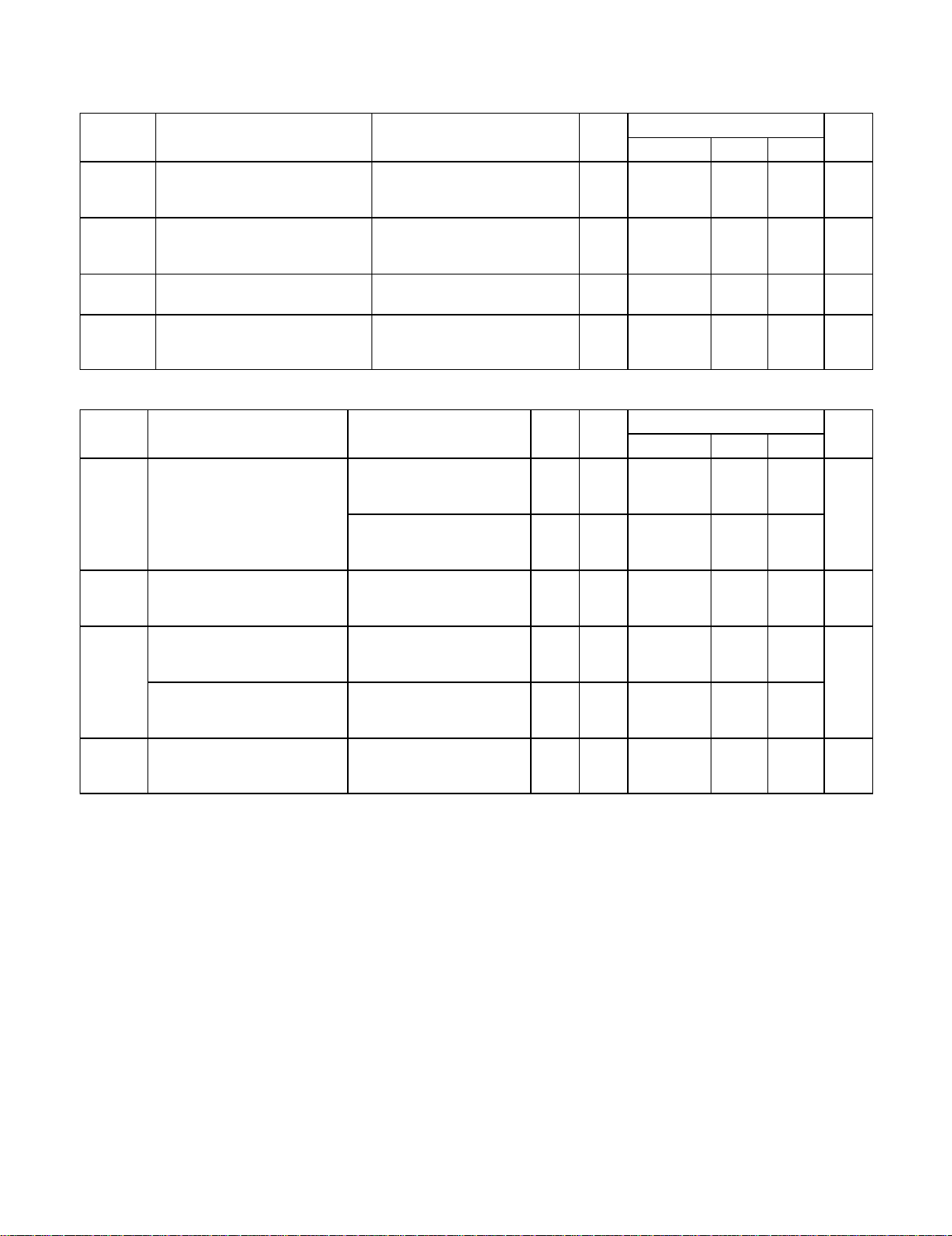
DC CHARACTERISTICS — Digital Section (Voltages Referenced to GND) V
Symbol Parameter Condition
V
Minimum High–Level Input Voltage,
IH
Ron = Per Spec 2.0
Channel–Select or Enable Inputs
V
Maximum Low–Level Input Voltage,
IL
Ron = Per Spec 2.0
Channel–Select or Enable Inputs
I
I
CC
Maximum Input Leakage Current,
in
Channel–Select or Enable Inputs
Maximum Quiescent Supply
Current (per Package)
Vin = VCC or GND,
V
= – 6.0 V
EE
Channel Select, Enable and
V
= VCC or GND; VEE = GND
IS
= 0 V VEE = – 6.0
V
IO
DC CHARACTERISTICS — Analog Section
Symbol Parameter Condition V
R
∆R
I
I
Maximum “ON” Resistance Vin = VIL or VIH; VIS = VCC to
on
V
; IS ≤ 2.0 mA
EE
(Figures 1, 2)
Vin = VIL or VIH; VIS = VCC or
V
(Endpoints); IS ≤ 2.0 mA
EE
(Figures 1, 2)
Maximum Difference in “ON”
on
Resistance Between Any Two
Channels in the Same Package
Maximum Off–Channel Leakage
off
Current, Any One Channel
Vin = VIL or VIH;
V
= 1/2 (VCC – VEE);
IS
I
≤ 2.0 mA
S
Vin = VIL or VIH;
V
= VCC – VEE;
IO
Switch Off (Figure 3)
Maximum Off–Channel HC4051
Leakage Current, HC4052
Common Channel HC4053
Maximum On–Channel HC4051
on
Leakage Current, HC4052
Channel–to–Channel HC4053
Vin = VIL or VIH;
V
= VCC – VEE;
IO
Switch Off (Figure 4)
Vin = VIL or VIH;
Switch–to–Switch =
– VEE; (Figure 5)
V
CC
= GND, Except Where Noted
EE
CC
V
4.5
6.0
4.5
6.0
Guaranteed Limit
–55 to 25°C ≤85°C ≤125°C
1.50
3.15
4.20
0.3
0.9
1.2
1.50
3.15
4.20
0.3
0.9
1.2
1.50
3.15
4.20
0.3
0.9
1.2
6.0 ±0.1 ± 1.0 ± 1.0 µA
6.0
6.0
2
8
20
80
40
160
Guaranteed Limit
CC
4.5
4.5
6.0
4.5
4.5
6.0
4.5
4.5
6.0
EE
0.0
– 4.5
– 6.0
0.0
– 4.5
– 6.0
0.0
– 4.5
– 6.0
190
120
100
150
100
80
30
12
10
240
150
125
190
125
100
35
15
12
280
170
140
230
140
115
40
18
14
–55 to 25°C ≤85°C ≤125°C
V
6.0 – 6.0 0.1 0.5 1.0
6.0
6.0
6.0
6.0
6.0
6.0
– 6.0
– 6.0
– 6.0
– 6.0
– 6.0
– 6.0
0.2
0.1
0.1
0.2
0.1
0.1
2.0
1.0
1.0
2.0
1.0
1.0
4.0
2.0
2.0
4.0
2.0
2.0
Unit
V
V
µA
Unit
Ω
Ω
µA
µA
Page 6
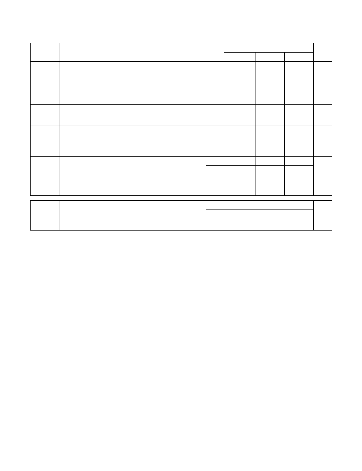
MC54/74HC4051 MC74HC4052 MC54/74HC4053
V
AC CHARACTERISTICS (C
= 50 pF, Input tr = tf = 6 ns)
L
Symbol Parameter
t
,
PLH
t
t
PLH
t
t
PLZ
t
PHZ
t
PZL
t
PZH
C
C
PHL
PHL
Maximum Propagation Delay, Channel–Select to Analog Output
(Figure 9)
,
Maximum Propagation Delay, Analog Input to Analog Output
(Figure 10)
,
Maximum Propagation Delay, Enable to Analog Output
(Figure 11)
,
Maximum Propagation Delay, Enable to Analog Output
(Figure 11)
Maximum Input Capacitance, Channel–Select or Enable Inputs 10 10 10 pF
in
Maximum Capacitance Analog I/O 35 35 35 pF
I/O
(All Switches Off) Common O/I: HC4051
C
Power Dissipation Capacitance (Figure 13)* HC4051
PD
Guaranteed Limit
370
74
63
60
12
10
290
58
49
345
69
59
130
80
50
465
93
79
75
15
13
364
73
62
435
87
74
130
80
50
550
110
94
90
18
15
430
86
73
515
103
87
130
80
50
HC4052
HC4053
CC
–55 to 25°C ≤85°C ≤125°C
V
2.0
4.5
6.0
2.0
4.5
6.0
2.0
4.5
6.0
2.0
4.5
6.0
Feedthrough 1.0 1.0 1.0
Typical @ 25°C, VCC = 5.0 V, VEE = 0 V
45
HC4052
HC4053
80
45
Unit
ns
ns
ns
ns
pF
Page 7
MC54/74HC4051 MC74HC4052 MC54/74HC4053
V
V
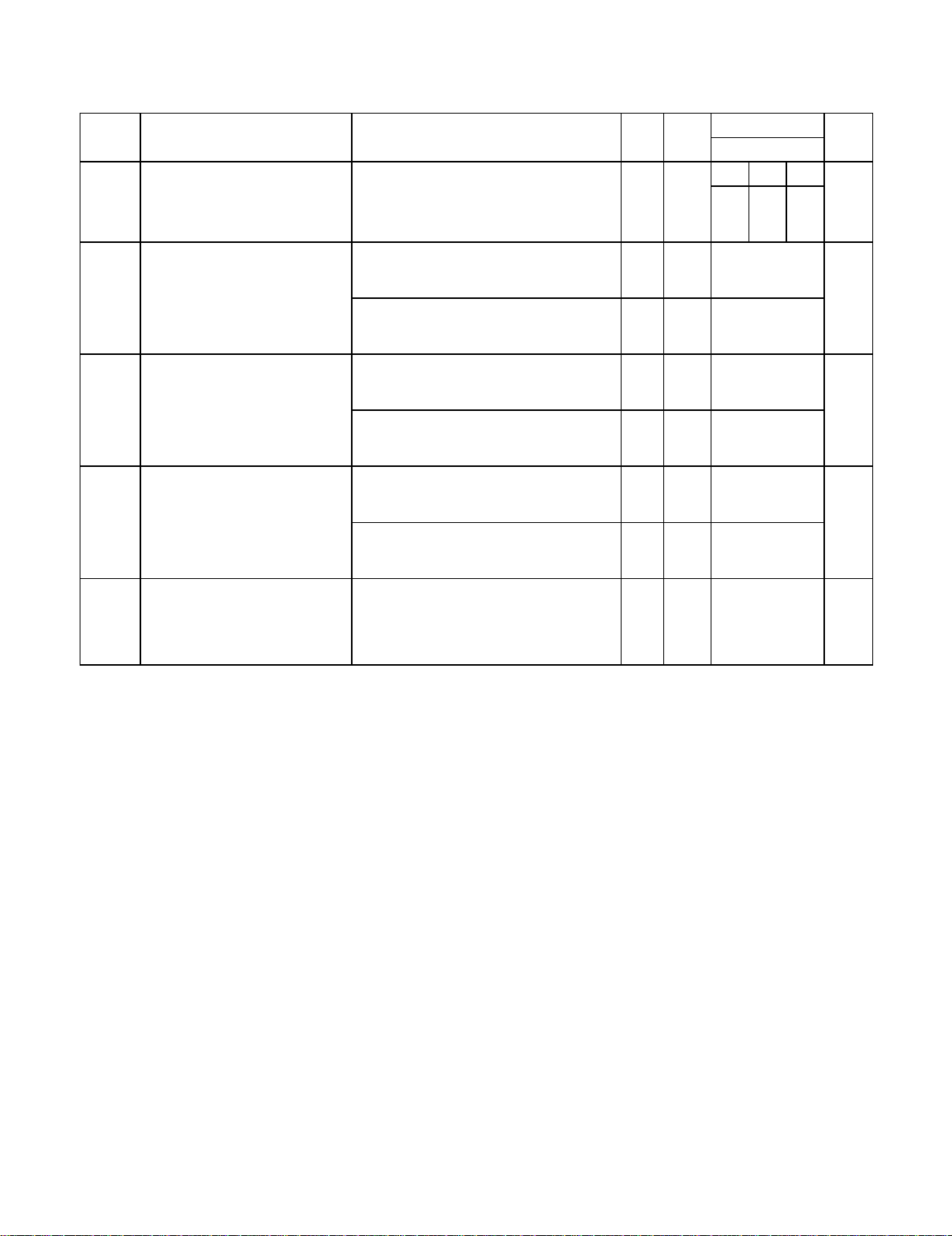
ADDITIONAL APPLICATION CHARACTERISTICS (GND = 0 V)
Symbol Parameter Condition
BW Maximum On–Channel Bandwidth
or Minimum Frequency Response
(Figure 6)
— Off–Channel Feedthrough Isolation
(Figure 7)
— Feedthrough Noise.
Channel–Select Input to Common
I/O (Figure 8)
— Crosstalk Between Any Two
Switches (Figure 12)
(Test does not apply to HC4051)
THD Total Harmonic Distortion
(Figure 14)
*Limits not tested. Determined by design and verified by qualification.
fin = 1MHz Sine Wave; Adjust fin Voltage to
Obtain 0dBm at VOS; Increase fin Frequency
Until dB Meter Reads –3dB;
= 50Ω, CL = 10pF
R
L
fin = Sine Wave; Adjust fin Voltage to Obtain
0dBm at V
IS
fin = 10kHz, RL = 600Ω, CL = 50pF
fin = 1.0MHz, RL = 50Ω, CL = 10pF
Vin ≤ 1MHz Square Wave (tr = tf = 6ns);
Adjust R
at Setup so that IS = 0A;
L
Enable = GND R
fin = Sine Wave; Adjust fin Voltage to Obtain
0dBm at V
IS
fin = 10kHz, RL = 600Ω, CL = 50pF
fin = 1.0MHz, RL = 50Ω, CL = 10pF
fin = 1kHz, RL = 10kΩ, CL = 50pF
THD = THD
measured
– THD
VIS = 4.0VPP sine wave
V
V
IS
= 600Ω, CL = 50pF
L
RL = 10kΩ, CL = 10pF
source
= 8.0VPP sine wave
IS
= 11.0VPP sine wave
CC
V
2.25
4.50
6.00
2.25
4.50
6.00
2.25
4.50
6.00
2.25
4.50
6.00
2.25
4.50
6.00
2.25
4.50
6.00
2.25
4.50
6.00
2.25
4.50
6.00
EE
V
–2.25
–4.50
–6.00
–2.25
–4.50
–6.00
–2.25
–4.50
–6.00
–2.25
–4.50
–6.00
–2.25
–4.50
–6.00
–2.25
–4.50
–6.00
–2.25
–4.50
–6.00
–2.25
–4.50
–6.00
Limit*
25°C
‘51 ‘52 ‘53
80
95
95
95
120
120
120
80
80
–50
–50
–50
–40
–40
–40
25
105
135
35
145
190
–50
–50
–50
–60
–60
–60
0.10
0.08
0.05
Unit
MHz
dB
mV
dB
PP
%
Page 8
MC54/74HC4051 MC74HC4052 MC54/74HC4053
300
250
200
150
100
, ON RESISTANCE (OHMS)
on
R
50
0
0 0.25 0.50 0.75 1.0 1.25 1.5 1.75 2.0 2.25
V
, INPUT VOLTAGE (VOLTS), REFERENCED TO V
IS
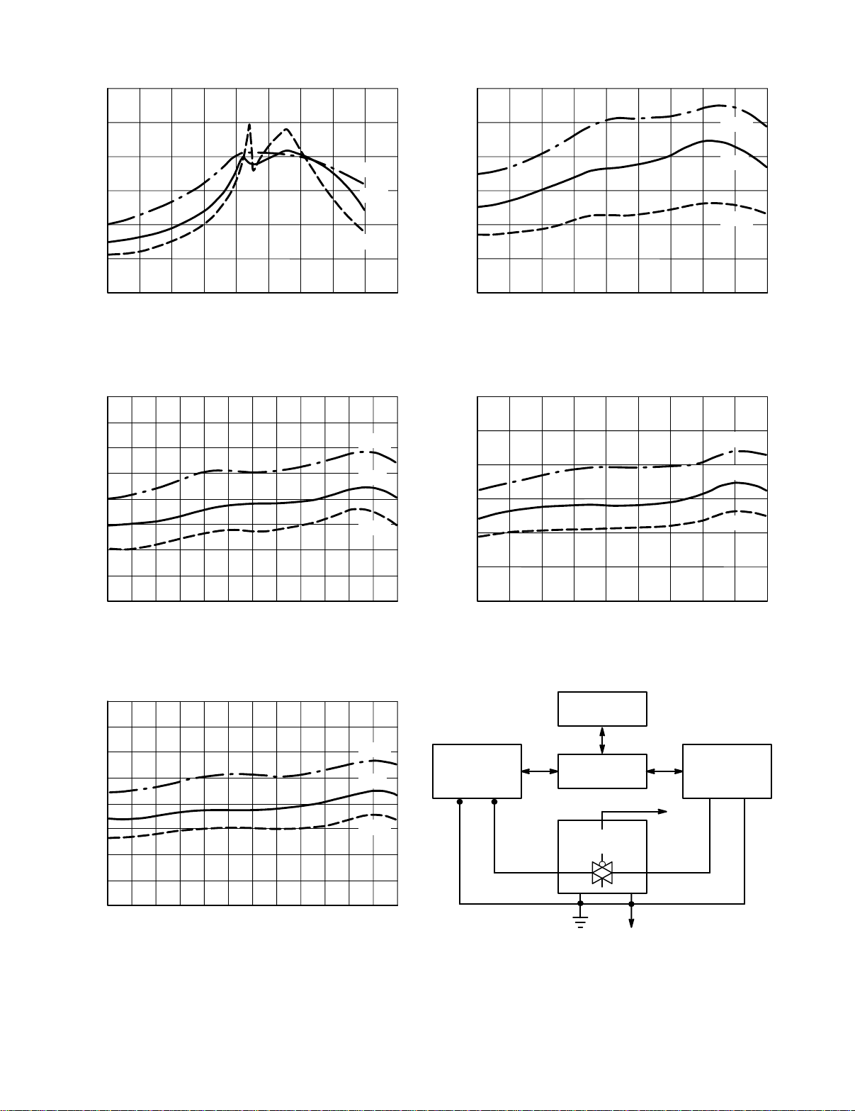
Figure 1a. Typical On Resistance, V
– VEE = 2.0 V Figure 1b. Typical On Resistance, V
CC
120
105
90
75
60
125°C
25°C
-55°C
EE
125°C
25°C
120
100
80
60
40
, ON RESISTANCE (OHMS)
on
R
20
0
0 0.5 1.0 1.5 2.0 2.5 3.0 3.5 4.0 4.5
V
, INPUT VOLTAGE (VOLTS), REFERENCED TO V
IS
– VEE = 4.5 V
CC
90
75
60
45
125°C
25°C
-55°C
EE
125°C
25°C
45
, ON RESISTANCE (OHMS)
30
on
R
15
0
0 0.5 1.0 1.5 2.0 2.5 3.0 3.5 4.0 4.5
, INPUT VOLTAGE (VOLTS), REFERENCED TO V
V
IS
Figure 1c. T ypical On Resistance, V
80
70
60
50
40
30
, ON RESISTANCE (OHMS)
20
on
R
10
0
1.0 2.0
0
3.0 4.0 5.0 6.0 7.0 8.0 9.0 10.0 11.0 12.0
, INPUT VOLTAGE (VOLTS), REFERENCED TO V
V
IS
-55°C
5.0 5.5 6.0
EE
– VEE = 6.0 V Figure 1d. Typical On Resistance, V
CC
30
, ON RESISTANCE (OHMS)
on
R
15
0
0 1.0 2.0 3.0 4.0 5.0 6.0 7.0 8.0 9.0
, INPUT VOLTAGE (VOLTS), REFERENCED TO V
V
IS
PLOTTER
125°C
25°C
PROGRAMMABLE
POWER
SUPPLY
MINI COMPUTER
+-
-55°C
DEVICE
UNDER TEST
ANALOG IN COMMON OUT
GND
EE
-55°C
EE
– VEE = 9.0 V
CC
DC ANALYZER
V
CC
V
EE
Figure 1e. T ypical On Resistance, V
– VEE = 12.0 V Figure 2. On Resistance Test Set–Up
CC
Page 9
MC54/74HC4051 MC74HC4052 MC54/74HC4053
V
CC
V
CC
V
EE
16
OFF
V
CC
A
NC
V
IH
OFF
6
COMMON O/I
7
8
V
EE
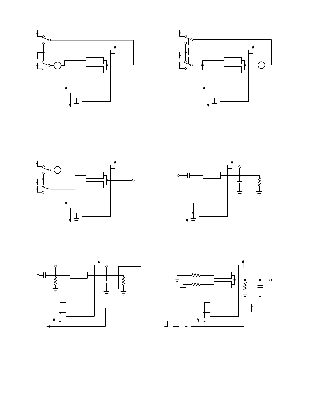
Figure 3. Maximum Off Channel Leakage Current,
Any One Channel, Test Set–Up
V
CC
A
ON
V
EE
V
CC
ANALOG I/O
OFF
16
COMMON O/I
V
CC
N/C
V
CC
V
CC
OFF
OFF
16
COMMON O/I
V
EE
V
CC
ANALOG I/O
V
IH
6
7
8
V
EE
Figure 4. Maximum Off Channel Leakage Current,
Common Channel, Test Set–Up
V
CC
V
OS
ON
16
dB
METER
R
CL*
L
0.1µF
f
in
V
IL
6
7
8
V
EE
Figure 5. Maximum On Channel Leakage Current,
Channel to Channel, Test Set–Up
V
CC
V
IS
0.1µF
f
in
OFF
R
L
V
OS
16
dB
METER
R
CL*
L
6
7
8
V
VIL or V
EE
IH
CHANNEL SELECT
*Includes all probe and jig capacitance
Figure 7. Off Channel Feedthrough Isolation,
Test Set–Up
6
7
8
V
EE
*Includes all probe and jig capacitance
Figure 6. Maximum On Channel Bandwidth,
Test Set–Up
V
CC
R
L
16
ON/OFF
ANALOG I/O
OFF/ON
R
L
6
7
≤ 1 MHz
V
GND
CC
V
in
t
= tf = 6 ns
r
8
V
EE
CHANNEL SELECT
11
*Includes all probe and jig capacitance
Figure 8. Feedthrough Noise, Channel Select to
Common Out, Test Set–Up
COMMON O/I
R
L
V
CC
TEST
POINT
CL*
Page 10
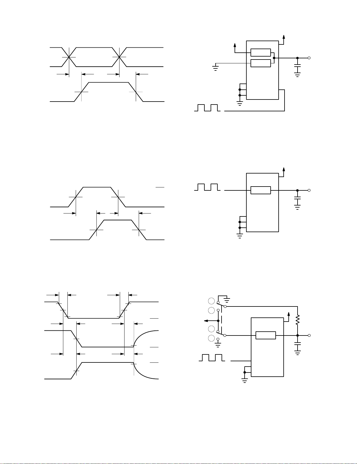
MC54/74HC4051 MC74HC4052 MC54/74HC4053
V
CC
CHANNEL
SELECT
ANALOG
OUT
t
PLH
50%
50%
t
GND
PHL
V
CC
ANALOG I/O
V
CC
16
ON/OFF
OFF/ON
COMMON O/I
TEST
POINT
CL*
6
7
8
CHANNEL SELECT
*Includes all probe and jig capacitance
Figure 9a. Propagation Delays, Channel Select
to Analog Out
ANALOG
ANALOG
OUT
IN
t
PLH
50%
50%
Figure 10a. Propagation Delays, Analog In
to Analog Out
t
ENABLE
ANALOG
OUT
ANALOG
OUT
f
50%
50%
t
t
PZL
PZH
t
t
t
PHZ
r
PLZ
Figure 11a. Propagation Delays, Enable to
Analog Out
90%
50%
10%
10%
90%
t
PHL
V
CC
GND
HIGH
IMPEDANCE
V
OL
V
OH
HIGH
IMPEDANCE
V
CC
GND
Figure 9b. Propagation Delay, Test Set–Up Channel
Select to Analog Out
V
CC
16
ANALOG I/O
ON
COMMON O/I
TEST
POINT
CL*
6
7
8
*Includes all probe and jig capacitance
Figure 10b. Propagation Delay, Test Set–Up
Analog In to Analog Out
POSITION 1 WHEN TESTING t
1
2
V
CC
1
2
POSITION 2 WHEN TESTING t
ANALOG I/O
ON/OFF
ENABLE
6
V
16
7
8
AND t
PHZ
PZH
AND t
PLZ
PZL
CC
1kΩ
TEST
POINT
CL*
Figure 11b. Propagation Delay, Test Set–Up
Enable to Analog Out
Page 11
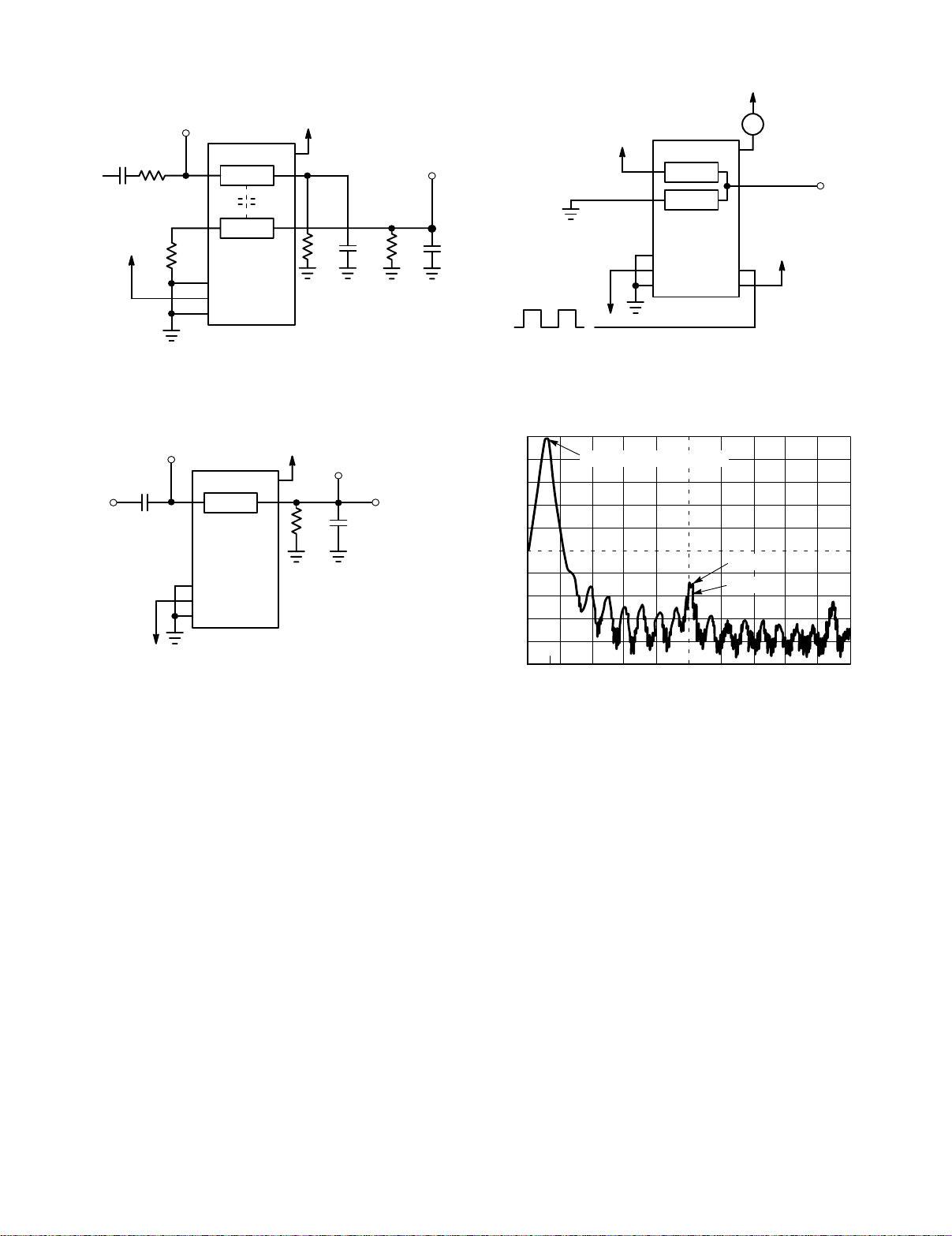
MC54/74HC4051 MC74HC4052 MC54/74HC4053
V
V
IS
V
CC
ANALOG I/O
V
EE
ON/OFF
OFF/ON
6
7
8
CHANNEL SELECT
Test Set–Up
R
0.1µF
L
V
EE
R
L
6
7
8
*Includes all probe and jig capacitance
f
in
Figure 12. Crosstalk Between Any Two
ON
OFF
16
R
L
CL*
V
OS
R
L
CL*
Figure 13. Power Dissipation Capacitance,
Switches, Test Set–Up
CC
A
16
COMMON O/I
11
NC
V
CC
dB
0
-10
-20
-30
-40
-50
-60
-70
-80
-90
-100
FUNDAMENTAL FREQUENCY
DEVICE
SOURCE
1.0 2.0 3.125
FREQUENCY (kHz)
V
IS
0.1µF
f
in
6
7
8
V
EE
V
CC
16
ON
*Includes all probe and jig capacitance
V
OS
TO
DISTORTION
CL*
METER
R
L
Figure 14a. Total Harmonic Distortion, Test Set–Up Figure 14b. Plot, Harmonic Distortion
APPLICATIONS INFORMATION
The Channel Select and Enable control pins should be at
V
or GND logic levels. VCC being recognized as a logic
CC
high and GND being recognized as a logic low. In this example:
= +5V = logic high
V
CC
GND = 0V = logic low
The maximum analog voltage swings are determined by
the supply voltages V
voltage should not exceed V
analog voltage should not go below V
difference between V
and VEE. The positive peak analog
CC
CC
. Similarly, the negative peak
CC
. In this example, the
EE
and VEE is ten volts. Therefore,
using the configuration of Figure 15, a maximum analog signal of ten volts peak–to–peak can be controlled. Unused
analog inputs/outputs may be left floating (i.e., not connected). However, tying unused analog inputs and outputs to
V
or GND through a low value resistor helps minimize
CC
crosstalk and feedthrough noise that may be picked up by an
unused switch.
Although used here, balanced supplies are not a require-
ment. The only constraints on the power supplies are that:
– GND = 2 to 6 volts
V
CC
V
– GND = 0 to –6 volts
EE
V
– VEE = 2 to 12 volts
CC
and VEE ≤ GND
When voltage transients above V
and/or below VEE are
CC
anticipated on the analog channels, external Germanium or
Schottky diodes (Dx) are recommended as shown in Figure
16. These diodes should be able to absorb the maximum
anticipated current surges during clipping.
Page 12
MC54/74HC4051 MC74HC4052 MC54/74HC4053
+5V
-5V
+5V
V
V
V
CC
CC
D
16
x
D
x
V
EE
ANALOG
SIGNAL
-5V
V
+5V
16
ANALOG
ON
6
7
8
SIGNAL
11
10
TO EXTERNAL CMOS
CIRCUITRY 0 to 5V
DIGITAL SIGNALS
9
+5V
-5V
CC
D
x
ON/OFF
D
x
V
EE
7
8
V
EE
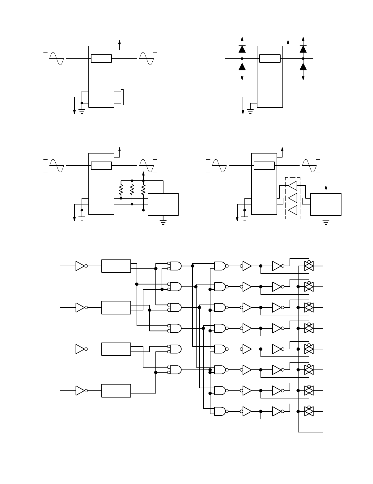
Figure 15. Application Example Figure 16. External Germanium or
Schottky Clipping Diodes
+5V
16
ANALOG
EE
SIGNAL
ON/OFF
ANALOG
SIGNAL
+5V
+5V
V
EE
+5V
V
ANALOG
EE
SIGNAL
ON/OFF
R*R R
6
11
7
10
8
V
EE
9
* 2K ≤ R ≤ 10K
LSTTL/NMOS
CIRCUITRY
V
EE
6
7
8
16
11
10
9
+5V
ANALOG
SIGNAL
HCT
BUFFER
+5V
V
EE
+5V
LSTTL/NMOS
CIRCUITRY
a. Using Pull–Up Resistors b. Using HCT Interface
ENABLE
Figure 17. Interfacing LSTTL/NMOS to CMOS Inputs
11
A
10
B
9
C
6
LEVEL
SHIFTER
LEVEL
SHIFTER
LEVEL
SHIFTER
LEVEL
SHIFTER
13
X0
14
X1
15
X2
12
X3
1
X4
5
X5
2
X6
4
X7
Figure 18. Function Diagram, HC4051
3
X
Page 13
MC54/74HC4051 MC74HC4052 MC54/74HC4053
ENABLE
10
A
9
B
6
LEVEL
SHIFTER
LEVEL
SHIFTER
LEVEL
SHIFTER
12
X0
14
X1
15
X2
11
X3
13
X
1
Y0
5
Y1
2
Y2
4
Y3
3
Y
ENABLE
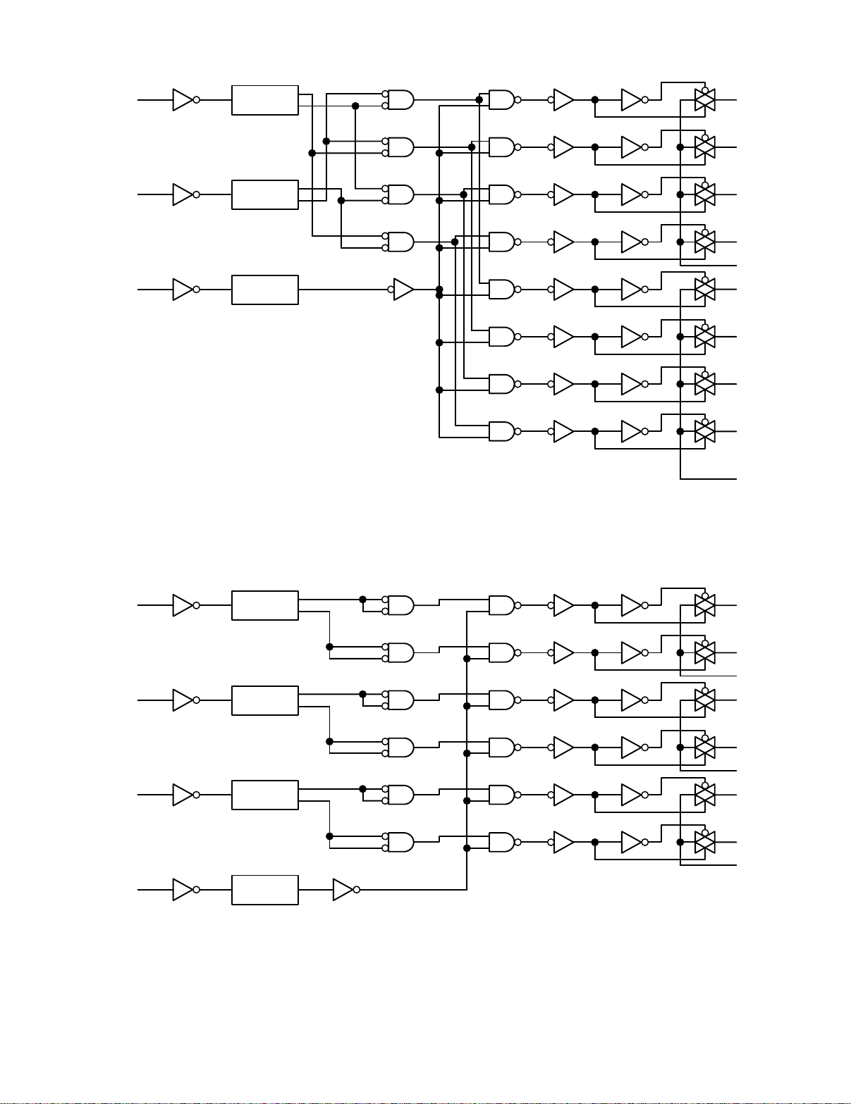
Figure 19. Function Diagram, HC4052
11
A
10
B
9
C
6
LEVEL
SHIFTER
LEVEL
SHIFTER
LEVEL
SHIFTER
LEVEL
SHIFTER
13
X1
12
X0
14
X
1
Y1
2
Y0
15
Y
3
Z1
5
Z0
4
Z
Figure 20. Function Diagram, HC4053
Page 14
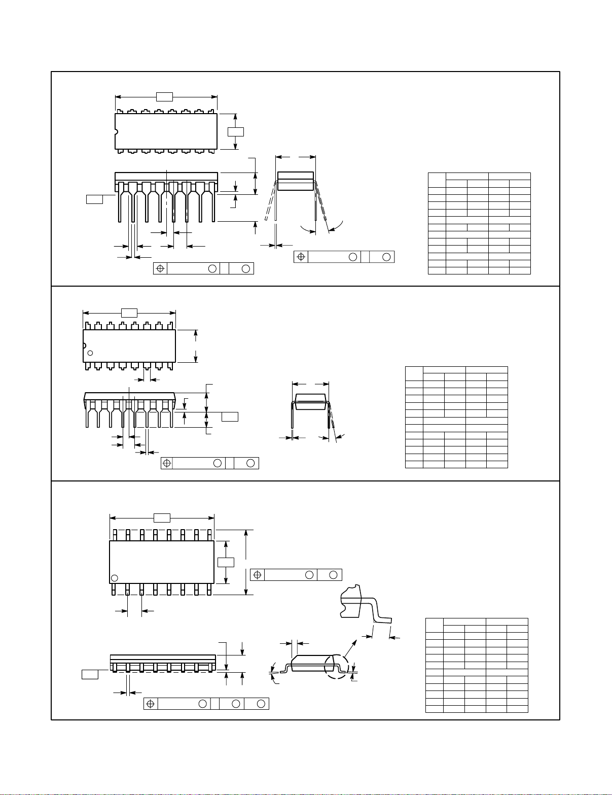
MC54/74HC4051 MC74HC4052 MC54/74HC4053
OUTLINE DIMENSIONS
J SUFFIX
–A
–
916
–B
18
–T
SEATING
–
PLANE
N
E
F
G
D 16 PL
M
–A
0.25 (0.010) T A
–
916
B
18
F
C
S
–T
–
H
G
D
16 PL
K
M M
TA0.25 (0.010)
CERAMIC PACKAGE
CASE 620–10
–
C
K
S
N SUFFIX
PLASTIC PACKAGE
CASE 648–08
SEATING
PLANE
J
ISSUE V
L
M
J
16 PL
0.25 (0.010) T B
ISSUE R
L
NOTES:
1. DIMENSIONING AND TOLERANCING PER
ANSI Y14.5M, 1982.
2. CONTROLLING DIMENSION: INCH.
3. DIMENSION L TO CENTER OF LEAD WHEN
FORMED PARALLEL.
4. DIM F MAY NARROW TO 0.76 (0.030) WHERE
THE LEAD ENTERS THE CERAMIC BODY.
INCHES MILLIMETERS
MIN MINMAX MAX
DIM
0.750
A
B
0.240
C
D
0.015
0.050 BSC
E
F
0.055
0.100 BSC
G
J
0.008
K
0.125
0.300 BSC
M
S
NOTES:
1. DIMENSIONING AND TOLERANCING PER ANSI
2. CONTROLLING DIMENSION: INCH.
3. DIMENSION L TO CENTER OF LEADS WHEN
4. DIMENSION B DOES NOT INCLUDE MOLD FLASH.
5. ROUNDED CORNERS OPTIONAL.
M
L
M
N0°0.020
Y14.5M, 1982.
FORMED PARALLEL.
INCHES MILLIMETERS
MIN MINMAX MAX
DIM
A
0.740
B
0.250
C
0.145
D
0.015
F
0.040
G
0.100 BSC
H
0.050 BSC
J
0.008
K
0.110
L
0.295
M
0°
S
0.020
0.770
0.270
0.175
0.021
0.070
0.015
0.130
0.305
0.040
10°
0.785
0.295
0.200
0.020
0.065
0.015
0.170
15°
0.040
18.80
6.35
3.69
0.39
1.02
0.21
2.80
7.50
0.51
0°
19.05
6.10
0.39
1.40
0.21
3.18
0°
0.51
19.55
6.85
4.44
0.53
1.77
2.54 BSC
1.27 BSC
0.38
3.30
7.74
10°
1.01
1.27 BSC
2.54 BSC
7.62 BSC
19.93
7.49
5.08
0.50
1.65
0.38
4.31
15°
1.01
–T
SEATING
–
PLANE
D SUFFIX
PLASTIC SOIC PACKAGE
P 8 PL
0.25 (0.010) B
CASE 751B–05
ISSUE J
M M
R X 45°
M
NOTES:
1. DIMENSIONING AND TOLERANCING PER ANSI
Y14.5M, 1982.
2. CONTROLLING DIMENSION: MILLIMETER.
3. DIMENSIONS A AND B DO NOT INCLUDE
MOLD PROTRUSION.
4. MAXIMUM MOLD PROTRUSION 0.15 (0.006)
PER SIDE.
5. DIMENSION D DOES NOT INCLUDE DAMBAR
PROTRUSION. ALLOWABLE DAMBAR
PROTRUSION SHALL BE 0.127 (0.005) TOTAL
IN EXCESS OF THE D DIMENSION AT
MAXIMUM MATERIAL CONDITION.
MILLIMETERS INCHES
MIN MINMAX MAX
DIM
A
F
J
9.80
B
3.80
C
1.35
D
0.35
F
0.40
1.27 BSC 0.050 BSC
G
J
0.19
K
0.10
M
0°
P
5.80
R
0.25
10.00
4.00
1.75
0.49
1.25
0.25
0.25
6.20
0.50
0.386
0.393
0.150
0.157
0.054
0.068
0.014
0.019
0.016
0.049
0.008
0.009
0.004
0.009
0°
0.229
0.010
0.244
0.019
7°
7°
–A
–
916
–B
1
–
8
G
K
C
16PL
D
0.25 (0.010) T B A
M
S S
Page 15
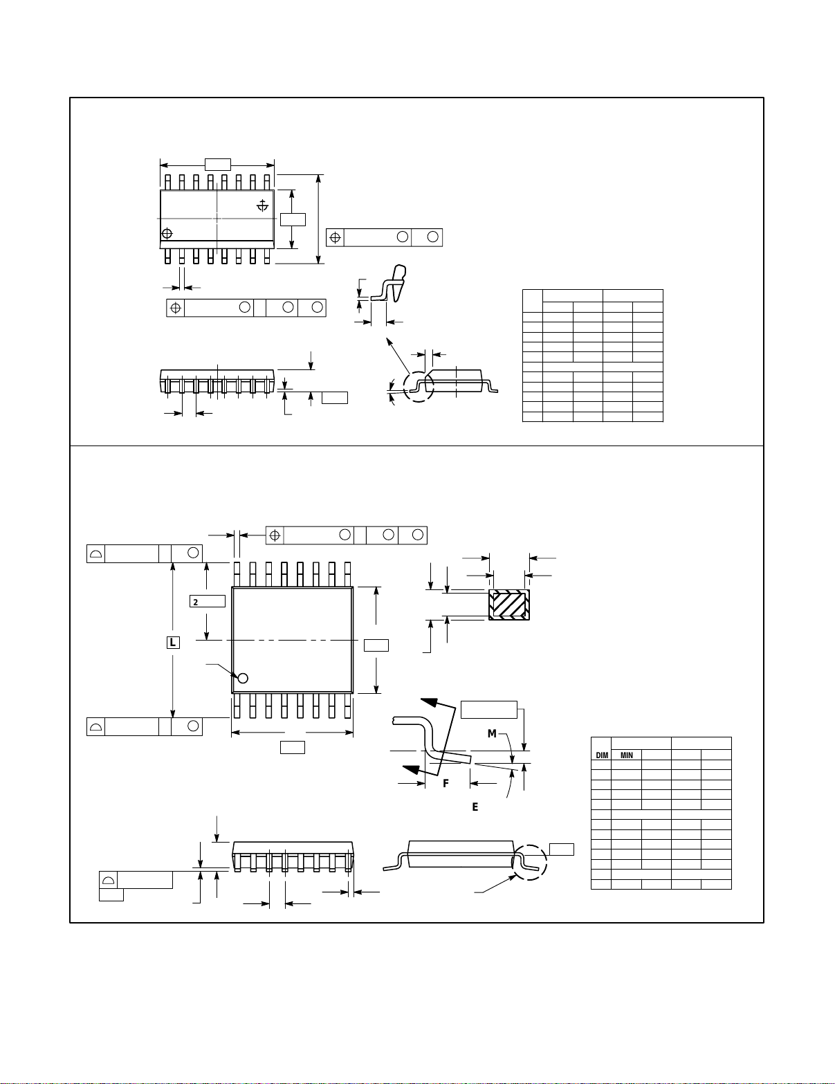
ÇÇ
ÇÇ
–A–
16 9
D16X
0.010 (0.25) B
M
T
G14X
–B– P8X
81
S
A
K
MC54/74HC4051 MC74HC4052 MC54/74HC4053
OUTLINE DIMENSIONS
DW SUFFIX
PLASTIC SOIC PACKAGE
CASE 751G–02
ISSUE A
M
J
F
M
C
S
–T–
SEATING
PLANE
0.010 (0.25)
NOTES:
1. DIMENSIONING AND TOLERANCING
PER ANSI Y14.5M, 1982.
2. CONTROLLING DIMENSION: MILLIMETER.
3. DIMENSIONS A AND B DO NOT INCLUDE MOLD
PROTRUSION.
4. MAXIMUM MOLD PROTRUSION 0.15 (0.006) PER
M
B
R
X 45
SIDE.
5. DIMENSION D DOES NOT INCLUDE DAMBAR
PROTRUSION. ALLOWABLE DAMBAR
PROTRUSION SHALL BE 0.13 (0.005) TOTAL IN
EXCESS OF D DIMENSION AT MAXIMUM
MATERIAL CONDITION.
DIM MIN MAX MIN MAX
A 10.15 10.45 0.400 0.411
B 7.40 7.60 0.292 0.299
C 2.35 2.65 0.093 0.104
D 0.35 0.49 0.014 0.019
F 0.50 0.90 0.020 0.035
G 1.27 BSC 0.050 BSC
J 0.25 0.32 0.010 0.012
K 0.10 0.25 0.004 0.009
M 0 7 0 7
P 10.05 10.55 0.395 0.415
R 0.25 0.75 0.010 0.029
INCHESMILLIMETERS
0.10 (0.004)
–T–
SEATING
PLANE
L
U0.15 (0.006) T
PIN 1
IDENT.
U0.15 (0.006) T
D
S
2X L/2
S
DT SUFFIX
PLASTIC TSSOP PACKAGE
CASE 948F–01
T
U
B
–U–
ISSUE O
S
S
J
N
N
H
J1
F
DETAIL E
DETAIL E
K
K1
SECTION N–N
0.25 (0.010)
M
NOTES:
1. DIMENSIONING AND TOLERANCING PER ANSI
Y14.5M, 1982.
2. CONTROLLING DIMENSION: MILLIMETER.
3. DIMENSION A DOES NOT INCLUDE MOLD FLASH.
PROTRUSIONS OR GATE BURRS. MOLD FLASH OR
GATE BURRS SHALL NOT EXCEED 0.15 (0.006) PER
SIDE.
4. DIMENSION B DOES NOT INCLUDE INTERLEAD
FLASH OR PROTRUSION. INTERLEAD FLASH OR
PROTRUSION SHALL NOT EXCEED
0.25 (0.010) PER SIDE.
5. DIMENSION K DOES NOT INCLUDE DAMBAR
PROTRUSION. ALLOWABLE DAMBAR PROTRUSION
SHALL BE 0.08 (0.003) TOTAL IN EXCESS OF THE K
DIMENSION AT MAXIMUM MATERIAL CONDITION.
6. TERMINAL NUMBERS ARE SHOWN FOR
REFERENCE ONLY.
7. DIMENSION A AND B ARE TO BE DETERMINED AT
DATUM PLANE -W-.
INCHESMILLIMETERS
–W–
DIM MIN MAX MIN MAX
A 4.90 5.10 0.193 0.200
B 4.30 4.50 0.169 0.177
C --- 1.20 --- 0.047
D 0.05 0.15 0.002 0.006
F 0.50 0.75 0.020 0.030
G 0.65 BSC 0.026 BSC
H 0.18 0.28 0.007 0.011
J 0.09 0.20 0.004 0.008
J1 0.09 0.16 0.004 0.006
K 0.19 0.30 0.007 0.012
K1 0.19 0.25 0.007 0.010
L 6.40 BSC 0.252 BSC
M 0 8 0 8
16X REFK
0.10 (0.004) V
16
1
M
9
8
A
–V–
C
G
Page 16
MC54/74HC4051 MC74HC4052 MC54/74HC4053
ON Semiconductor and are trademarks of Semiconductor Components Industries, LLC (SCILLC). SCILLC reserves the right to make changes
without further notice to any products herein. SCILLC makes no warranty, representation or guarantee regarding the suitability of its products for any particular
purpose, nor does SCILLC assume any liability arising out of the application or use of any product or circuit, and specifically disclaims any and all liability,
including without limitation special, consequential or incidental damages. “Typical” parameters which may be provided in SCILLC data sheets and/or
specifications can and do vary in different applications and actual performance may vary over time. All operating parameters, including “Typicals” must be
validated for each customer application by customer’s technical experts. SCILLC does not convey any license under its patent rights nor the rights of others.
SCILLC products are not designed, intended, or authorized for use as components in systems intended for surgical implant into the body, or other applications
intended to support or sustain life, or for any other application in which the failure of the SCILLC product could create a situation where personal injury or
death may occur. Should Buyer purchase or use SCILLC products for any such unintended or unauthorized application, Buyer shall indemnify and hold
SCILLC and its officers, employees, subsidiaries, affiliates, and distributors harmless against all claims, costs, damages, and expenses, and reasonable
attorney fees arising out of, directly or indirectly, any claim of personal injury or death associated with such unintended or unauthorized use, even if such claim
alleges that SCILLC was negligent regarding the design or manufacture of the part. SCILLC is an Equal Opportunity/Affirmative Action Employer.
PUBLICATION ORDERING INFORMATION
Literature Fulfillment:
Literature Distribution Center for ON Semiconductor
P.O. Box 5163, Denver, Colorado 80217 USA
Phone: 303–675–2175 or 800–344–3860 Toll Free USA/Canada
Fax: 303–675–2176 or 800–344–3867 Toll Free USA/Canada
Email: [email protected]
N. American Technical Support: 800–282–9855 Toll Free USA/Canada
JAPAN: ON Semiconductor, Japan Customer Focus Center
4–32–1 Nishi–Gotanda, Shinagawa–ku, Tokyo, Japan 141–0031
Phone: 81–3–5740–2700
Email: [email protected]
ON Semiconductor Website: http://onsemi.com
For additional information, please contact your local
Sales Representative.
MC74HC4051/D
 Loading...