

Page 1
SEMICONDUCTOR TECHNICAL DATA
1
REV 6
Motorola, Inc. 1995
10/95
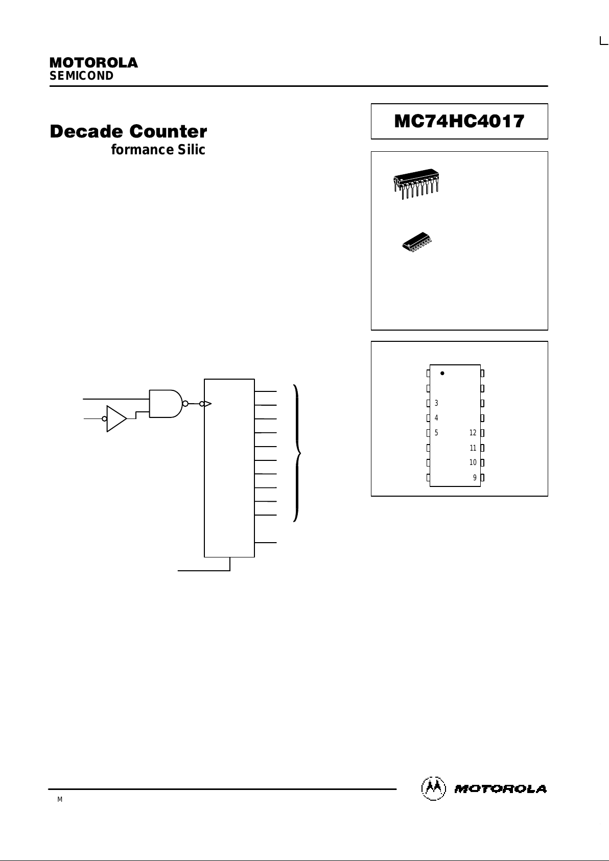
High–Performance Silicon–Gate CMOS
The MC74HC4017 is identical i n pinout t o the s tandard C MOS
MC14017B. The device inputs are compatible with standard CMOS outputs;
with pullup resistors, they are compatible with LSTTL outputs.
The HC4017 uses a five stage Johnson counter and decoding logic to
provide high–speed operation. This device also has an active–high, as well
as active–low clock input.
• Output Drive Capability: 10 LSTTL Loads
• Outputs Directly Interface to CMOS, NMOS, and TTL
• Operating Voltage Range: 2 to 6 V
• Low Input Current: 1 µA
• High Noise Immunity Characteristic of CMOS Devices
• In Compliance with the Requirements Defined by JEDEC Standard
No. 7A
• Chip Complexity: 176 FETs or 44 Equivalent Gates
LOGIC DIAGRAM
DECADE
OUTPUTS
PIN 16 = V
CC
PIN 8 = GND
CLOCK
ENABLE
CARRY OUT
RESET
CLOCK
Q0
Q1
Q2
Q3
Q4
Q5
Q6
Q7
Q8
Q9
15
3
2
4
7
1
5
6
9
14
13
11
12
10
PIN ASSIGNMENT
13
14
15
16
9
10
11
125
4
3
2
1
8
7
6
CARRY OUT
CLOCK ENABLE
CLOCK
RESET
V
CC
Q8
Q4
Q9
Q2
Q0
Q1
Q5
GND
Q3
Q7
Q6
D SUFFIX
SOIC PACKAGE
CASE 751B–05
N SUFFIX
PLASTIC PACKAGE
CASE 648–08
1
16
1
16
ORDERING INFORMATION
MC74HCXXXXN
MC74HCXXXXD
Plastic
SOIC
Page 2
MC74HC4017
MOTOROLA High–Speed CMOS Logic Data
DL129 — Rev 6
2
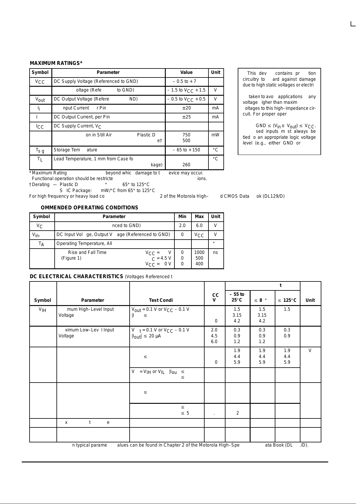
MAXIMUM RATINGS*
Symbol
Parameter
Value
Unit
V
CC
DC Supply Voltage (Referenced to GND)
– 0.5 to + 7.0
V
V
in
DC Input Voltage (Referenced to GND)
– 1.5 to VCC + 1.5
V
V
out
DC Output Voltage (Referenced to GND)
– 0.5 to VCC + 0.5
V
I
in
DC Input Current, per Pin
± 20
mA
I
out
DC Output Current, per Pin
± 25
mA
I
CC
DC Supply Current, VCC and GND Pins
± 50
mA
P
D
Power Dissipation in Still Air Plastic DIP†
SOIC Package†
750
500
mW
T
stg
Storage Temperature
– 65 to + 150
_
C
T
L
Lead Temperature, 1 mm from Case for 10 Seconds
(Plastic DIP or SOIC Package)
260
_
C
*Maximum Ratings are those values beyond which damage to the device may occur.
Functional operation should be restricted to the Recommended Operating Conditions.
†Derating — Plastic DIP: – 10 mW/_C from 65_ to 125_C
SOIC Package: – 7 mW/_C from 65_ to 125_C
For high frequency or heavy load considerations, see Chapter 2 of the Motorola High–Speed CMOS Data Book (DL129/D).
RECOMMENDED OPERATING CONDITIONS
Symbol
Parameter
Min
Max
Unit
V
CC
DC Supply Voltage (Referenced to GND)
2.0
6.0
V
Vin, V
out
DC Input Voltage, Output Voltage (Referenced to GND)
0
V
CC
V
T
A
Operating Temperature, All Package Types
– 55
+ 125
_
C
tr, t
f
Input Rise and Fall Time VCC = 2.0 V
(Figure 1) VCC = 4.5 V
VCC = 6.0 V
0
0
0
1000
500
400
ns
DC ELECTRICAL CHARACTERISTICS (Voltages Referenced to GND)
Guaranteed Limit
Symbol
Parameter
Test Conditions
V
CC
V
– 55 to
25_C
v
85_Cv 125_C
Unit
V
IH
Minimum High–Level Input
Voltage
V
out
= 0.1 V or VCC – 0.1 V
|I
out
| v 20 µA
2.0
4.5
6.0
1.5
3.15
4.2
1.5
3.15
4.2
1.5
3.15
4.2
V
V
IL
Maximum Low–Level Input
Voltage
V
out
= 0.1 V or VCC – 0.1 V
|I
out
| v 20 µA
2.0
4.5
6.0
0.3
0.9
1.2
0.3
0.9
1.2
0.3
0.9
1.2
V
V
OH
Minimum High–Level Output
Voltage
Vin = VIH or V
IL
|I
out
| v 20 µA
2.0
4.5
6.0
1.9
4.4
5.9
1.9
4.4
5.9
1.9
4.4
5.9
V
Vin = VIH or VIL|I
out
| v 4.0 mA
|I
out
| v 5.2 mA
4.5
6.0
3.98
5.48
3.84
5.34
3.70
5.20
V
OL
Maximum Low–Level Output
Voltage
Vin = VIH or V
IL
|I
out
| v 20 µA
2.0
4.5
6.0
0.1
0.1
0.1
0.1
0.1
0.1
0.1
0.1
0.1
V
Vin = VIH or VIL|I
out
| v 4.0 mA
|I
out
| v 5.2 mA
4.5
6.0
0.26
0.26
0.33
0.33
0.40
0.40
I
in
Maximum Input Leakage Current
Vin = VCC or GND
6.0
± 0.1
± 1.0
± 1.0
µA
I
CC
Maximum Quiescent Supply
Current (per Package)
Vin = VCC or GND
I
out
= 0 µA
6.0
8
80
160
µA
NOTE: Information on typical parametric values can be found in Chapter 2 of the Motorola High–Speed CMOS Data Book (DL129/D).
This device contains protection
circuitry to guard against damage
due to high static voltages or electric
fields. However, precautions must
be taken to avoid applications of any
voltage higher than maximum rated
voltages to this high–impedance circuit. For proper operation, Vin and
V
out
should be constrained to the
range GND v (Vin or V
out
) v VCC.
Unused inputs must always be
tied to an appropriate logic voltage
level (e.g., either GND or VCC).
Unused outputs must be left open.
Page 3
MC74HC4017
High–Speed CMOS Logic Data
DL129 — Rev 6
3 MOTOROLA
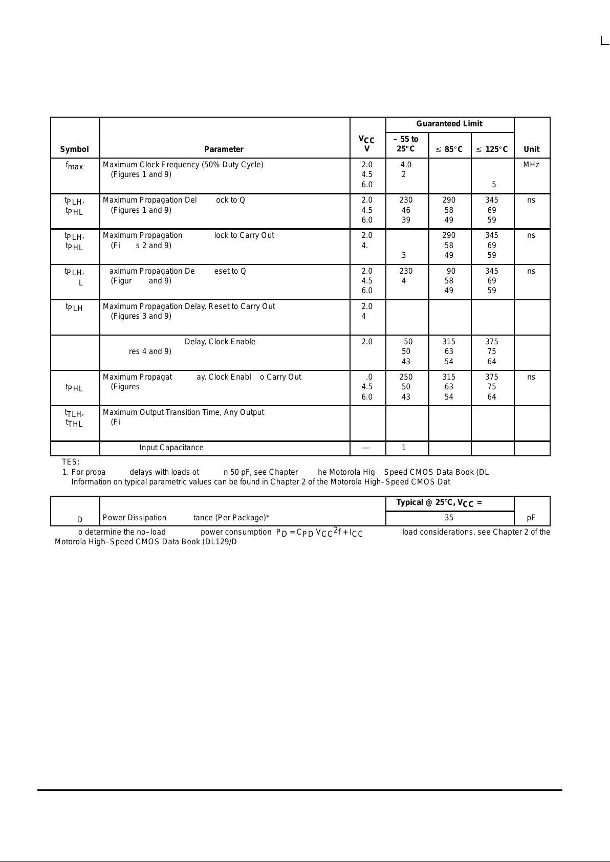
AC ELECTRICAL CHARACTERISTICS (C
L
= 50 pF, Input tr = tf = 6 ns)
Guaranteed Limit
Symbol
Parameter
V
CC
V
– 55 to
25_C
v
85_Cv 125_C
Unit
f
max
Maximum Clock Frequency (50% Duty Cycle)
(Figures 1 and 9)
2.0
4.5
6.0
4.0
20
24
3.2
16
19
2.6
13
15
MHz
t
PLH
,
t
PHL
Maximum Propagation Delay, Clock to Q
(Figures 1 and 9)
2.0
4.5
6.0
230
46
39
290
58
49
345
69
59
ns
t
PLH
,
t
PHL
Maximum Propagation Delay, Clock to Carry Out
(Figures 2 and 9)
2.0
4.5
6.0
230
46
39
290
58
49
345
69
59
ns
t
PLH
,
t
PHL
Maximum Propagation Delay, Reset to Q
(Figures 3 and 9)
2.0
4.5
6.0
230
46
39
290
58
49
345
69
59
ns
t
PLH
Maximum Propagation Delay, Reset to Carry Out
(Figures 3 and 9)
2.0
4.5
6.0
230
46
39
290
58
49
345
69
59
ns
t
PLH
,
t
PHL
Maximum Propagation Delay, Clock Enable to Q
(Figures 4 and 9)
2.0
4.5
6.0
250
50
43
315
63
54
375
75
64
ns
t
PLH
,
t
PHL
Maximum Propagation Delay, Clock Enable to Carry Out
(Figures 5 and 9)
2.0
4.5
6.0
250
50
43
315
63
54
375
75
64
ns
t
TLH
,
t
THL
Maximum Output Transition Time, Any Output
(Figures 8 and 9)
2.0
4.5
6.0
75
15
13
95
19
16
110
22
19
ns
C
in
Maximum Input Capacitance
—
10
10
10
pF
NOTES:
1. For propagation delays with loads other than 50 pF, see Chapter 2 of the Motorola High–Speed CMOS Data Book (DL129/D).
2. Information on typical parametric values can be found in Chapter 2 of the Motorola High–Speed CMOS Data Book (DL129/D).
Typical @ 25°C, VCC = 5.0 V
C
PD
Power Dissipation Capacitance (Per Package)*
35
pF
*Used to determine the no–load dynamic power consumption: PD = CPD V
CC
2
f + ICC VCC. For load considerations, see Chapter 2 of the
Motorola High–Speed CMOS Data Book (DL129/D).
Page 4

MC74HC4017
MOTOROLA High–Speed CMOS Logic Data
DL129 — Rev 6
4
TIMING REQUIREMENTS (Input t
r
= tf = 6 ns)t
Guaranteed Limit
Symbol
Parameter
V
CC
V
– 55 to
25_C
v
85_Cv 125_C
Unit
t
su
Minimum Setup Time, Clock Enable to Clock
(Figure 6)
2.0
4.5
6.0
50
10
9
65
13
11
75
15
13
ns
t
su
Minimum Setup Time, Clock Enable to Clock (Inhibit Count)
(Figure 6)
2.0
4.5
6.0
50
10
9
65
13
11
75
15
13
ns
t
h
Minimum Hold Time, Clock to Clock Enable
(Figure 6)
2.0
4.5
6.0
50
10
9
65
13
11
75
15
13
ns
t
rec
Minimum Recovery Time, Reset to Clock
(Figure 7)
2.0
4.5
6.0
100
20
17
125
25
21
150
30
26
ns
t
w
Minimum Pulse Width, Clock Input
(Figure 2)
2.0
4.5
6.0
80
16
14
100
20
17
120
24
20
ns
t
w
Minimum Pulse Width, Reset Input
(Figure 3)
2.0
4.5
6.0
80
16
14
100
20
17
120
24
20
ns
t
w
Minimum Pulse Width, Clock Enable Input
(Figure 4)
2.0
4.5
6.0
80
16
14
100
20
17
120
24
20
ns
tr, t
f
Maximum Input Rise and Fall Times
(Figure 1)
2.0
4.5
6.0
1000
500
400
1000
500
400
1000
500
400
ns
NOTE: Information on typical parametric values can be found in Chapter 2 of the Motorola High–Speed CMOS Data Book (DL129/D).
FUNCTION TABLE
Clock
Clock
Enable
Reset Output State*
L X L no change
X H L no change
X X H reset counter, Q0 = H, Q1–Q9 = L, C0 = H
L L advance to next state
X L no change
X L no change
H L advance to next state
X = Don’t care
*Carry Out = H for Q0, Q1, Q2, Q3, or Q4 = H; Carry Out = L otherwise.
PIN DESCRIPTIONS
INPUTS
Clock (Pin 14)
Counter clock input. While Clock Enable is low, a low–to–
high transition on this input advances the counter to its next
state.
Reset (Pin 15)
Asynchronous counter reset input. A high level at this input
initializes the counter and forces Q0 and Carry Out to a high,
Q1–Q9 are forced to a low level.
Clock Enable (Pin 13)
Active–low clock enable input. A low level on this input allows the device to count. A high level on this input inhibits the
counting operation. T his input m ay also b e used as a
negative–edge clock i nput. using Clock ( Pin 14) as a n
active–high enable pin.
OUTPUTS
Q0–Q9 (Pins 3, 2, 4, 7, 10, 1, 5, 6, 9, 11)
Decoded decade counter outputs. Each of these outputs is
high for one clock period only.
Carry Out (Pin 12)
Cascading output pin. This output is used either as a cascading output or a symmetrical divide–by–ten output. This
output goes low when a count of five is reached and high
when the counter advances to zero or when reset. When the
counters are cascaded this output provides a rising–edge
signal for the clock input of the next counter stage.
Page 5

MC74HC4017
High–Speed CMOS Logic Data
DL129 — Rev 6
5 MOTOROLA
SWITCHING WAVEFORMS
t
r
t
f
90%
50%
10%
V
CC
GND
t
THL
t
PHL
t
PLH
1/f
max
t
TLH
Q1–Q9
Q0, CARRY OUT
Q
t
su
Q0–Q9,
CARRY OUT
t
rec
Figure 1.
Figure 2.
Figure 3.
Figure 4.
Figure 5.
Figure 6.
Figure 7.
Figure 8.
CLOCK
ENABLE
CARRY
OUT
RESET
CLOCK
CLOCK
CLOCK
ENABLE
CLOCK
CLOCK
ENABLE
CARRY
OUT
RESET
CLOCK
90%
50%
10%
V
CC
GND
V
CC
GND
V
CC
GND
V
CC
GND
50%
50%
t
w
t
w
t
PLH
t
PHL
t
w
t
PLH
t
PHL
90%
10%
t
THL
t
TLH
50%
50%
50%
50%
VALID
t
h
V
CC
GND
V
CC
GND
V
CC
GND
V
CC
GND
V
CC
GND
50%
50%
50%
50%
t
PHL
t
PLH
Q
50%
t
PLH
50%
50%
t
w
t
PHL
*Includes all probe and jig capacitance
Figure 9. Test Circuit
CL*
TEST POINT
DEVICE
UNDER
TEST
OUTPUT
Page 6

MC74HC4017
MOTOROLA High–Speed CMOS Logic Data
DL129 — Rev 6
6
TIMIING DIAGRAM
CLOCK
ENABLE
CARRY
OUT
RESET
CLOCK
Q0
Q1
Q2
Q3
Q4
Q5
Q6
Q7
Q8
Q9
Page 7

MC74HC4017
High–Speed CMOS Logic Data
DL129 — Rev 6
7 MOTOROLA
15
RESET
CLOCK
CLOCK
ENABLE
Q0
CARRY
OUT
3
2
4
7
1
5
6
9
EXPANDED LOGIC DIAGRAM
D Q
C Q
R
14
13
D Q
C Q
R
D Q
C Q
R
D Q
C Q
R
D Q
C Q
R
Q1
Q2
Q3
Q4
Q5
Q6
Q7
Q8
Q9
11
12
10
Page 8

MC74HC4017
MOTOROLA High–Speed CMOS Logic Data
DL129 — Rev 6
8
OSC.
(NO FEEDBACK REQUIRED)
1/6 HC04
OUTPUT
BUFFER
(OPTIONAL TO PREVENT SPURIOUS RESET.)
V
CC
HC4017
Q5
Q1
Q0
Q2
Q6
Q7
Q3
GND
RESET
CLOCK
CARRY OUT
Q9
Q4
Q8
1
2
3
4
5
6
7
8 9
10
11
12
13
14
15
16
÷
9
÷
10
TYPICAL APPLICATIONS
Figure 10. ÷2 Through ÷ 10 Circuit
CLOCK
ENABLE
C
R
CE
Q0 Q1 Q8 Q9
Figure 11. Counter Expansion
8 DECODED
OUTPUTS
HC08
FIRST STAGE INTERMEDIATE STAGES
V
CC
÷
4
÷
8
÷
5
÷
2
÷
6
÷
7
÷
3
HC4017 HC4017 HC4017
CLOCK
8 DECODED
OUTPUTS
9 DECODED
OUTPUTS
R R
HC08
LAST STAGE
C
CE
Q0 Q1 Q8 Q9
C
CE
Q1 Q8 Q9
Figure 10 shows a divide by 2 through 10 circuit using one HC4017. Please note that since Reset is asynchronous, the
output pulse widths are narrow.
Figure 11 shows a technique for cascading the counters to extend the number of decoded output states. Decoded outputs
are sequential within each stage and from stage to stage, with no dead time (except propagation delay).
Page 9

MC74HC4017
High–Speed CMOS Logic Data
DL129 — Rev 6
9 MOTOROLA
OUTLINE DIMENSIONS
N SUFFIX
PLASTIC PACKAGE
CASE 648–08
ISSUE R
MIN MINMAX MAX
INCHES MILLIMETERS
DIM
A
B
C
D
F
G
H
J
K
L
M
S
18.80
6.35
3.69
0.39
1.02
0.21
2.80
7.50
0
°
0.51
19.55
6.85
4.44
0.53
1.77
0.38
3.30
7.74
10
°
1.01
0.740
0.250
0.145
0.015
0.040
0.008
0.110
0.295
0
°
0.020
0.770
0.270
0.175
0.021
0.070
0.015
0.130
0.305
10
°
0.040
NOTES:
1. DIMENSIONING AND TOLERANCING PER ANSI
Y14.5M, 1982.
2. CONTROLLING DIMENSION: INCH.
3. DIMENSION L TO CENTER OF LEADS WHEN
FORMED PARALLEL.
4. DIMENSION B DOES NOT INCLUDE MOLD FLASH.
5. ROUNDED CORNERS OPTIONAL.
2.54 BSC
1.27 BSC
0.100 BSC
0.050 BSC
–A
–
B
1 8
916
F
H
G
D
16 PL
S
C
–T
–
SEATING
PLANE
K
J
M
L
T A0.25 (0.010)
M M
0.25 (0.010) T B A
M
S S
MIN MINMAX MAX
MILLIMETERS INCHES
DIM
A
B
C
D
F
G
J
K
M
P
R
9.80
3.80
1.35
0.35
0.40
0.19
0.10
0
°
5.80
0.25
10.00
4.00
1.75
0.49
1.25
0.25
0.25
7
°
6.20
0.50
0.386
0.150
0.054
0.014
0.016
0.008
0.004
0
°
0.229
0.010
0.393
0.157
0.068
0.019
0.049
0.009
0.009
7
°
0.244
0.019
1.27 BSC 0.050 BSC
NOTES:
1. DIMENSIONING AND TOLERANCING PER ANSI
Y14.5M, 1982.
2. CONTROLLING DIMENSION: MILLIMETER.
3. DIMENSIONS A AND B DO NOT INCLUDE
MOLD PROTRUSION.
4. MAXIMUM MOLD PROTRUSION 0.15 (0.006)
PER SIDE.
5. DIMENSION D DOES NOT INCLUDE DAMBAR
PROTRUSION. ALLOWABLE DAMBAR
PROTRUSION SHALL BE 0.127 (0.005) TOTAL
IN EXCESS OF THE D DIMENSION AT
MAXIMUM MATERIAL CONDITION.
1
8
916
–A
–
–B
–
D 16 PL
K
C
G
–T
–
SEATING
PLANE
R X 45°
M
J
F
P 8 PL
0.25 (0.010) B
M M
D SUFFIX
PLASTIC SOIC PACKAGE
CASE 751B–05
ISSUE J
How to reach us:
USA/EUROPE: Motorola Literature Distribution; JAPAN: Nippon Motorola Ltd.; Tatsumi–SPD–JLDC, Toshikatsu Otsuki,
P.O. Box 20912; Phoenix, Arizona 85036. 1–800–441–2447 6F Seibu–Butsuryu–Center, 3–14–2 Tatsumi Koto–Ku, Tokyo 135, Japan. 03–3521–8315
MFAX: RMFAX0@email.sps.mot.com –TOUCHTONE (602) 244–6609 HONG KONG: Motorola Semiconductors H.K. Ltd.; 8B Tai Ping Industrial Park,
INTERNET: http://Design–NET.com 51 Ting Kok Road, Tai Po, N.T., Hong Kong. 852–26629298
Motorola reserves the right to make changes without further notice to any products herein. Motorola makes no warranty , representation or guarantee regarding
the suitability of its products for any particular purpose, nor does Motorola assume any liability arising out of the application or use of any product or circuit,
and specifically disclaims any and all liability, including without limitation consequential or incidental damages. “T ypical” parameters can and do vary in different
applications. All operating parameters, including “T ypicals” must be validated for each customer application by customer’s technical experts. Motorola does
not convey any license under its patent rights nor the rights of others. Motorola products are not designed, intended, or authorized for use as components in
systems intended for surgical implant into the body, or other applications intended to support or sustain life, or for any other application in which the failure of
the Motorola product could create a situation where personal injury or death may occur. Should Buyer purchase or use Motorola products for any such
unintended or unauthorized application, Buyer shall indemnify and hold Motorola and its officers, employees, subsidiaries, affiliates, and distributors harmless
against all claims, costs, damages, and expenses, and reasonable attorney fees arising out of, directly or indirectly, any claim of personal injury or death
associated with such unintended or unauthorized use, even if such claim alleges that Motorola was negligent regarding the design or manufacture of the part.
Motorola and are registered trademarks of Motorola, Inc. Motorola, Inc. is an Equal Opportunity/Affirmative Action Employer.
MC74HC4017/D
*MC74HC4017/D*
◊
CODELINE
 Loading...