

Page 1
4-192
FAST AND LS TTL DATA
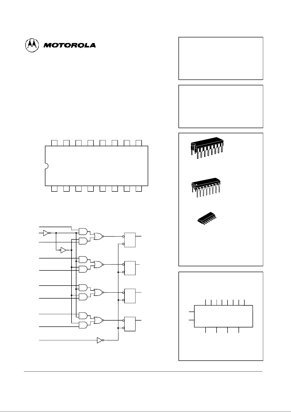
QUAD 2-PORT REGISTER
The MC54/74F399 is the logical equivalent of a quad 2-input multiplexer
feeding into four edge-triggered flip flops. A common Select input determines
which of the two 4-bit words is accepted. The selected data enters the flipflops on the rising edge of the clock. The MC54/74F399 is the 16-pin version
of the MC54/74F398, with only the Q outputs of the flip-flops available.
• Select Inputs from Two Data Sources
• Fully Positive Edge-Triggered Operation
6 7 81 2 3 4 5
10111314 12 91516
V
CCQdI0dI1dI1c
Q
c
I
0c
I
0aS
Q
a
I
1aI1b
Q
b
I
0b
CONNECTION DIAGRAM (TOP VIEW)
CP
GND
LOGIC DIAGRAM
NOTE:
This diagram is provided only for the understanding of logic operations and
should not be used to estimate propagation delays.
D
CP
Q
a
Q
b
Q
c
Q
d
I
0a
S
I
1a
I
0b
I
1b
I
0c
I
1c
I
0d
I
1d
CP
D
CP
D
CP
D
CP
J SUFFIX
CERAMIC
CASE 620-09
N SUFFIX
PLASTIC
CASE 648-08
16
1
16
1
ORDERING INFORMATION
MC54FXXXJ Ceramic
MC74FXXXN Plastic
MC74FXXXD SOIC
16
1
D SUFFIX
SOIC
CASE 751B-03
LOGIC SYMBOL
QUAD 2-PORT REGISTER
FAST SCHOTTKY TTL
MC54/74F399
I0a I1a I0b I1b I0c I1c I0d I
1d
S
CP
Q
a
Qb Q
c
Qd
3 4 6 5 11 12 14 13
2 7 10 15
1
9
VCC = PIN 16
GND = PIN 8
Page 2
4-193
FAST AND LS TTL DATA
MC54/74F399
FUNCTIONAL DESCRIPTION
The MC54/74F398 is a high-speed quad 2-port register. It
will select four bits of data from either of two sources (Ports)
under control of a common Select input (S). The selected data
is transferred to a 4-bit output register synchronous with the
LOW-to-HIGH transition of the Clock input (CP). The 4-bit D-
type output register is fully edge-triggered. The Data inputs
(I0x, I1x) and Select input (S) must be stable only a setup time
prior to and hold time after the LOW-to-HIGH transition of the
Clock input for predictable operation.
Inputs Output
S
I
0
I
1
Q
I
I
h
h
I
h
X
X
X
X
I
h
L
H
L
H
H = HIGH Voltage Level
L = LOW Voltage Level
h = HIGH Voltage Level one setup time prior to the LOW-to-HIGH clock transition
I = LOW Voltage Level one setup time prior to the LOW-to-HIGH clock transition
X = Don’t Care
FUNCTION TABLE
GUARANTEED OPERATING RANGES
Symbol Parameter Min Typ Max Unit
V
CC
Supply Voltage 54, 74 4.5 5.0 5.5 V
T
A
Operating Ambient Temperature Range 54 –55 25 125 °C
74 0 25 70
I
OH
Output Current High 54, 74 – 1.0 mA
I
OL
Output Current Low 54, 74 20 mA
DC CHARACTERISTICS OVER OPERATING TEMPERATURE RANGE (unless otherwise specified)
Limits
Symbol Parameter Min Typ Max Unit Test Conditions
V
IH
Input HIGH Voltage 2.0 V Guaranteed Input HIGH Voltage
V
IL
Input LOW Voltage 0.8 V Guaranteed Input LOW Voltage
V
IK
Input Clamp Diode Voltage –1.2 V IIN = –18 mA VCC = MIN
V
OH
Output HIGH Voltage 54, 74 2.5 3.4 V IOH = – 1.0 mA VCC = 4.5 V
74 2.7 3.4 V IOH = – 1.0 mA VCC = 4.75 V
V
OL
Output LOW Voltage 0.35 0.5 V IOL = 20 mA VCC = MIN
I
IH
Input HIGH Current 20 µA VIN = 2.7 V VCC = MAX
100 µA VIN = 7.0 V
I
IL
Input LOW Current –0.6 mA VIN = 0.5 V VCC = MAX
I
OS
Output Short Circuit Current (Note 2) –60 –150 mA V
OUT
= 0 V VCC = MAX
I
CC
Power Supply Current 22 34 mA VCC = MAX VIN = GND
CP =
NOTES:
1. For conditions shown as MIN or MAX, use the appropriate value specified under guaranteed operating ranges.
2. Not more than one output should be shorted at a time, nor for more than 1 second.
Page 3

4-194
FAST AND LS TTL DATA
MC54/74F399
AC CHARACTERISTICS
54/74F 54F 74F
TA = + 25°C TA = –55°C to +125°C TA = 0°C to 70°C
VCC = +5.0V VCC = 5.0 V ± 10% VCC = 5.0 V ± 10%
CL = 50 pF CL = 50 pF CL = 50 pF
Symbol Parameter Min Typ Max Min Max Min Max Unit
f
max
Maximum Clock Frequency 100 140 80 100 MHz
t
PLH
Propagation Delay 3.0 5.7 7.5 3.0 9.5 3.0 8.5 ns
t
PHL
CP to Q 3.0 6.8 9.5 3.0 11.5 3.0 10.0
AC OPERATING REQUIREMENTS
54/74F 54F 74F
TA = +25°C TA = –55°C to + 125°C TA = 0°C to 70°C
VCC = +5.0V VCC = 5.0 V ± 10% VCC = 5.0 V ± 10%
Symbol Parameter Min Typ Max Min Max Min Max Unit
ts(H) Setup Time, HIGH or LOW 3.0 4.5 3.0 ns
ts(L) In to CP 3.0 4.5 3.0
th(H) Hold Time, HIGH or LOW 1.0 1.5 1.0 ns
th(L) In to CP 1.0 1.5 1.0
ts(H) Setup Time, HIGH or LOW 7.5 9.5 8.5 ns
ts(L) S to CP 7.5 9.5 8.5
th(H) Hold Time, HIGH or LOW 0 0 0 ns
th(L) S to CP 0 0 0
tw(H) CP Pulse Width 4.0 4.0 4.0 ns
tw(L) HIGH or LOW 5.0 7.0 5.0
 Loading...