

Page 1

For:char
Printed on:Mon, Feb 6, 1995 09:49:57
From book:DL121CH4 (5) VIEW
Document:MC74F382 (5) VIEW
Last saved on:Fri, Feb 3, 1995 16:07:09
Page 2
4-184
FAST AND LS TTL DATA
4-BIT ARITHMETIC LOGIC UNIT
The MC54/74F382 performs three arithmetic and three logic operations on
two 4-bit words, A and B. Two additional Select input codes force the Function
outputs LOW or HIGH. An Overflow output is provided for convenience in twos
complement arithmetic. A Carry output is provided for ripple expansion. For
high-speed expansion using a Carry Lookahead Generator, refer to the F381
data sheet.
• Performs Six Arithmetic and Logic Functions
• Selectable Low (Clear) and High (Preset) Functions
• LOW Input Loading Minimizes Drive Requirements
• Carry Output for Ripple Expansion
• Overflow Output for Twos Complement Arithmetic
CONNECTION DIAGRAM
18 17 16 15 14 13
1 2 3 4 5 6
7
20 19
8
V
CC
A
1
A2B2A3B
3
C
n+4
C
n
OVR
B1A0B0S0S1S2F
0
9 10
F1GND
12 11
F3F
2
LOGIC SYMBOL
C
n
S
2
S
1
S
0
C
n+4
OVR
A
0
B3A3B2A
2
B0A1B
1
F
0
F
3
F
2
F
1
3 4 1 2 19 18 17 16
15
7
6
5
14
13
8 9 11 12
GUARANTEED OPERATING RANGES
Symbol Parameter Min Typ Max Unit
V
CC
Supply Voltage 54, 74 4.5 5.0 5.5 V
54 –55 25 125
TAOperating Ambient Temperature Range
74 0 25 70
°C
I
OH
Output Current — High 54, 74 –1.0 mA
I
OL
Output Current — Low 54, 74 20 mA
MC54/74F382
4-BIT ARITHMETIC LOGIC UNIT
FAST SCHOTTKY TTL
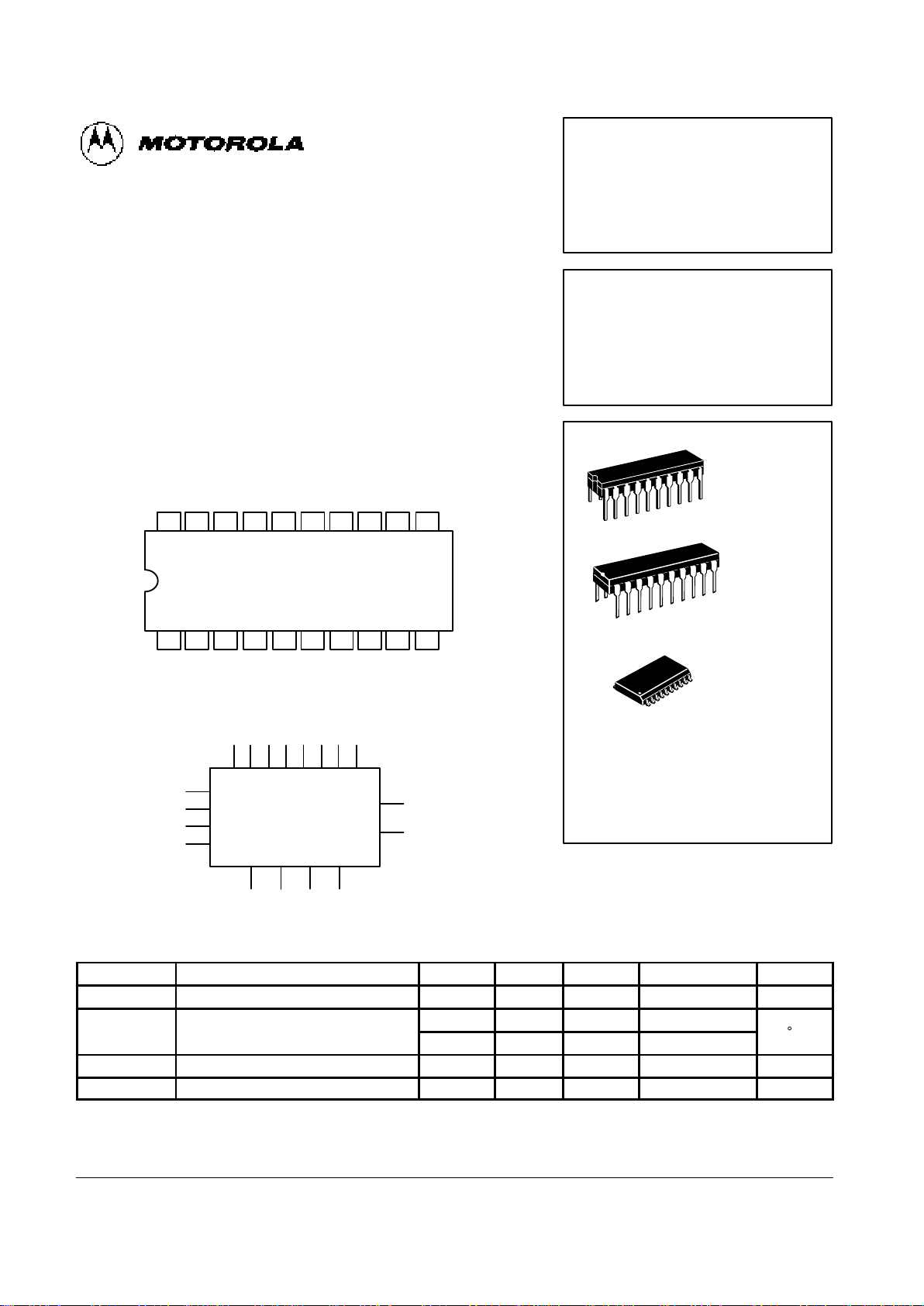
ORDERING INFORMATION
MC54FXXXJ Ceramic
MC74FXXXN Plastic
MC74FXXXDW SOIC
20
1
J SUFFIX
CERAMIC
CASE 732-03
20
1
N SUFFIX
PLASTIC
CASE 738-03
20
1
DW SUFFIX
SOIC
CASE 751D-03
Page 3

4-185
FAST AND LS TTL DATA
MC54/74F382
LOGIC DIAGRAM
Please note that this diagram is provided
only for the understanding of logic
operations and should not be used to
estimate propagation delays.
C
n
B
0
A
0
B
1
A
1
B
2
A
2
B
3
A
3
S
0
S
1
S
2
F
0
F
1
F
2
F
3
P
G
OVR
Cn+4
F381
ONLY
F382
ONLY
Page 4

4-186
FAST AND LS TTL DATA
MC54/74F382
DC CHARACTERISTICS OVER OPERATING TEMPERATURE RANGE (unless otherwise specified)
Limits
Symbol
Parameter
Min Typ Max
Unit
Test Conditions
V
IH
Input HIGH Voltage 2.0 V Guaranteed Input HIGH Voltage
V
IL
Input LOW Voltage 0.8 V Guaranteed Input LOW Voltage
V
IK
Input Clamp Diode Voltage –1.2 V IIN = –18 mA VCC = MIN
54, 74 2.5 3.4 V IOH = –1.0 mA VCC = 4.5 V
VOHOutput HIGH Voltage
74 2.7 3.4 V IOH = –1.0 mA VCC = 4.75 V
V
OL
Output LOW Voltage 0.35 0.5 V IOL = 20 mA VCC = MIN
20 µA VIN = 2.7 V
IIHInput HIGH Current
100 µA VIN = 7.0 V
VCC = MAX
Input LOW Current
S0–S2 Inputs
–0.6 mA
I
IL
Other Inputs
–2.4 mA
VIN = 0.5 V
VCC = MAX
Cn Input
–3.0 mA
I
OS
Output Short Circuit Current (Note 2) –60 –150 mA V
OUT
= 0 V VCC = MAX
I
CC
Power Supply Current 54 81 mA
S0, Cn = HIGH;
Other Inputs GND
VCC = MAX
NOTES:
1. For conditions such as MIN or MAX, use the appropriate value specified under guaranteed operating ranges.
2. Not more than one output should be shorted at a time, nor for more than 1 second.
FUNCTIONAL DESCRIPTION
Signals applied to the Select inputs S0–S2 determine the
mode of operation, as indicated in the Function Select Table.
An extensive listing of input and output levels is shown in the
Truth Table. The circuit performs the arithmetic functions for
either active HIGH or active LOW operands, with output levels
in the same convention. In the Subtract operating modes, it is
necessary to force a carry (HIGH for active HIGH operands,
LOW for active LOW operands) into the Cn input of the least
significant package. Ripple expansion is illustrated in Figure
1. The overflow output OVR is the Exclusive-OR of Cn + 3 and
C
n+4
; a HIGH signal on OVR indicates overflow in twos
complement operation. Typical delays for Figure 1 are given
in Figure 2.
FUNCTION SELECT TABLE
Select
S
0
S
1
S
2
Operation
L L L Clear
H L L B Minus A
L H L A Minus B
H H L A Plus B
L L H A⊕B
H L H A + B
L H H AB
H H H Preset
H = HIGH Voltage Level L = LOW Voltage Level
Page 5

4-187
FAST AND LS TTL DATA
MC54/74F382
Figure 1. 16-Bit Ripple Carry ALU Expansion
SELECT
3
3
C
in
A0–A3B0–B
3
A4–A7B4–B
7
A8–A11B8–B
11
A12–A15B12–B
15
4 4
A B
C
n
S
F382
Cn+4
OVR
F12–F
15
F0–F
3
F4–F
7
F8–F
11
OVERFLOW
C
out
3
4 4
A B
C
n
S
F382
Cn+4
3
4 4
A B
C
n
S
F382
Cn+4
3
4 4
A B
C
n
S
F382
Cn+4
Toward
Output
Path Segment
Toward
F
Output
Cn + 4, OVR
Ai or Bi to Cn +
4
6.5 ns 6.5 ns
Cn to Cn +
4
6.3 ns 6.3 ns
Cn to Cn +
4
6.3 ns 6.3 ns
Cn to F 8.1 —
Cn to Cn + 4, OVR — 8.0 ns
Total Delay 27.2 ns 27.1 ns
Figure 2. 16-Bit Delay Tabulation
AC CHARACTERISTICS
54/74F 54F 74F
TA = +25°C TA = –55 to +125°C TA = 0 to 70°C
VCC = +5.0 V VCC = 5.0 V ±10% VCC = 5.0 V ±10%
CL = 50 pF CL = 50 pF CL = 50 pF
Symbol
Parameter
Min Typ Max Min Max Min Max
Unit
t
PLH
Propagation Delay 3.0 8.1 12 3.0 15 3.0 13
t
PHL
Cn to F
i
2.5 5.7 8.0 2.5 11 2.5 9.0
ns
t
PLH
Propagation Delay 4.0 10.4 15 4.0 18 4.0 16
t
PHL
Any A or B to Any F 3.5 8.2 11 3.5 14 3.5 12
ns
t
PLH
Propagation Delay 6.0 11 15 6.0 21 6.0 16
t
PHL
Si to F
i
4.0 8.2 20.5 4.0 23.5 4.0 21.5
ns
t
PLH
Propagation Delay 3.5 6.0 8.5 3.5 11.5 3.5 9.5
t
PHL
Ai or Bi to Cn +
4
3.0 6.5 9.0 3.0 12.5 3.0 10.5
ns
t
PLH
Propagation Delay 7.0 12.5 16.5 7.0 19.5 7.0 17.5
t
PHL
Si to OVR or Cn +
4
4.5 9.0 12 4.5 15 4.5 13
ns
t
PLH
Propagation Delay 2.5 5.6 8.0 2.5 11 2.5 9.0
t
PHL
Cn to Cn +
4
2.5 6.3 9.0 2.5 12 2.5 10
ns
t
PLH
Propagation Delay 3.5 8.0 11 3.5 14 3.5 12
t
PHL
Cn to OVR 3.5 7.1 10 3.5 13 3.5 11
ns
t
PLH
Propagation Delay 6.5 11.5 15.5 6.5 18.5 6.5 16.5
t
PHL
Ai or Bi to OVR 5.5 8.0 10.5 5.5 13.5 5.5 11.5
ns
Page 6

4-188
FAST AND LS TTL DATA
MC54/74F382
TRUTH TABLE
INPUTS OUTPUTS
Function S
0
S1S
2
CnAnB
n
F
0
F
1
F
2
F
3
OVR Cn +
4
0 X X 0 0 0 0 1 1
CLEAR
0 0 0
1 X X 0 0 0 0 1 1
0 0 0 1 1 1 1 0 0
0 0 1 0 1 1 1 0 1
0 1 0 0 0 0 0 0 0
0 1 1 1 1 1 1 0 0
B MINUS A
100
1 0 0 0 0 0 0 0 1
1 0 1 1 1 1 1 0 1
1 1 0 1 0 0 0 0 0
1 1 1 0 0 0 0 0 1
0 0 0 1 1 1 1 0 0
0 0 1 0 0 0 0 0 0
0 1 0 0 1 1 1 0 1
0 1 1 1 1 1 1 0 0
A MINUS B
010
1 0 0 0 0 0 0 0 1
1 0 1 1 0 0 0 0 0
1 1 0 1 1 1 1 0 1
1 1 1 0 0 0 0 0 1
0 0 0 0 0 0 0 0 0
0 0 1 1 1 1 1 0 0
0 1 0 1 1 1 1 0 0
A PLUS B
0 1 1 0 1 1 1 0 1
110
1 0 0 1 0 0 0 0 0
1 0 1 0 0 0 0 0 1
1 1 0 0 0 0 0 0 1
1 1 1 1 1 1 1 0 1
X 0 0 0 0 0 0 0 0
X 0 1 1 1 1 1 0 0
A⊕B 0 0 1 0 1 0 1 1 1 1 0 0
X 1 1 0 0 0 0 1 1
1 1 0 1 1 1 1 1 1
X 0 0 0 0 0 0 0 0
X 0 1 1 1 1 1 0 0
A + B 1 0 1 X 1 0 1 1 1 1 0 0
0 1 1 1 1 1 1 0 0
1 1 1 1 1 1 1 1 1
X 0 0 0 0 0 0 1 1
X 0 1 0 0 0 0 0 0
AB 0 1 1 X 1 0 0 0 0 0 1 1
0 1 1 1 1 1 1 0 0
1 1 1 1 1 1 1 1 1
X 0 0 1 1 1 1 0 0
X 0 1 1 1 1 1 0 0
PRESET 1 1 1 X 1 0 1 1 1 1 0 0
0 1 1 1 1 1 1 0 0
1 1 1 1 1 1 1 1 1
1 = HIGH Voltage Level
0 = LOW Voltage Level
X = Immaterial
 Loading...