

Page 1

For:char
Printed on:Mon, Feb 6, 1995 09:48:26
From book:DL121CH4 (5) VIEW
Document:MC74F323 (5) VIEW
Last saved on:Fri, Feb 3, 1995 16:04:13
Page 2
4-150
FAST AND LS TTL DATA
8-INPUT SHIFT/STORAGE
REGISTER WITH SYNCHRONOUS
RESET AND COMMON I/O PINS
The MC74F323 is an 8-Bit Universal Shift/Storage Register with 3-state
outputs. Its function is similar to the F299 with the exception of Synchronous
Reset.
The parallel load inputs and flip-flop outputs are multiplexed to reduce the
total number of package pins. Separate outputs are provided for flip-flops Q
0
and Q7 to allow easy cascading. A separate active LOW Master Reset is used
to reset the register.
Four modes of operation are possible: hold (store), shift left, shift right and
parallel load. All modes are activated on the LOW-to-HIGH transition of the
clock.
• Common I/O For Reduced Pin Count
• Four Operation Modes: Shift Left, Shift Right, Parallel Load and Store
• Separate Continuous Inputs and Outputs from Q
0
and Q7 Allow Easy
Cascading
• Fully Synchronous Reset
• 3-State Outputs for Bus Oriented Applications
• Input Clamp Diodes Limit High-Speed Termination Effects
CONNECTION DIAGRAM
18 17 16 15 14 13
1 2 3 4 5 6
7
20 19
8
V
CC
S
0
S1DS7Q7I/O
7
I/O
3
I/O
5
I/O
1
OE
1OE2
I/O6I/O4I/O2I/O0Q
0
9 10
SR
GND
12 11
CP DS
0
GUARANTEED OPERATING RANGES
Symbol Parameter Min Typ Max Unit
V
CC
Supply Voltage 74 4.5 5.0 5.5 V
T
A
Operating Ambient Temperature Range 74 0 25 70 °C
I
OH
Output Current — High 74 –1.0/–3.0 mA
I
OL
Output Current — Low 74 20/24 mA
MC74F323
8-INPUT SHIFT/STORAGE
REGISTER WITH SYNCHRONOUS
RESET AND COMMON I/O PINS
FAST SCHOTTKY TTL
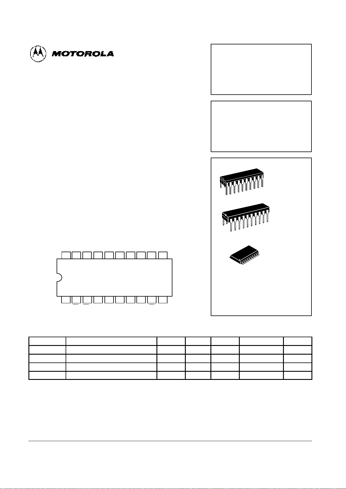
ORDERING INFORMATION
MC74FXXXJ Ceramic
MC74FXXXN Plastic
MC74FXXXDW SOIC
20
1
J SUFFIX
CERAMIC
CASE 732-03
20
1
N SUFFIX
PLASTIC
CASE 738-03
20
1
DW SUFFIX
SOIC
CASE 751D-03
Page 3

4-151
FAST AND LS TTL DATA
MC74F323
FUNCTION TABLE
Inputs
SR S
1
S
0
CP Response
L X X ↑ Synchronous Reset: Q0–Q7 = LOW
H H H ↑ Parallel Load: I/On º Q
n
H L H ↑ Shift Right: DS0 º Q0, Q0 º Q1, etc.
H H L ↑ Shift Left: DS7 º Q7, Q7 º Q6, etc.
H L L X Hold
H = HIGH Voltage Level
L = LOW Voltage Level
X = Don’t Care
↑ = LOW-to-HIGH clock transition.
FUNCTIONAL DESCRIPTION
The MC74F323 contains eight edge-triggered D-type
flips-flops and the interstage logic necessary to perform
synchronous reset, shift left, shift right, parallel load and hold
operations. The type of operation is determined by S0 and S1,
as shown in the Function Table. All flip-flop outputs are
brought out through 3-state buffers to separate I/O pins that
also serve as data inputs in the parallel load mode. Q0 and Q
7
are also brought out on other pins for expansion in serial
shifting of longer words.
A LOW signal on SR
overrides the Select inputs and allows
the flip-flops to be reset by the next rising edge of CP . All other
state changes are initiated by the LOW-to-HIGH CP transition.
Inputs can change when the clock is in either state provided
only that the recommended set-up and hold times, relative to
the rising edge of CP, are observed.
A HIGH signal on either OE
1
or OE2 disables the 3-state
buffers and puts the I/O pins in the high impedance state. In
this condition the shift, hold, load and reset operations can still
occur. The 3-state buffers are also disabled by HIGH signals
on both S0 and S1 in preparation for a parallel load operation.
DC CHARACTERISTICS OVER OPERATING TEMPERATURE RANGE
(Unless otherwise specified)
Limits
Symbol
Parameter
Min Typ Max
Unit
Test Conditions
V
IH
Input HIGH Voltage 2.0 V Guaranteed Input HIGH Voltage
V
IL
Input LOW Voltage 0.8 V Guaranteed Input LOW Voltage
V
IK
Input Clamp Diode Voltage –1.2 V VCC = MIN, IIN = –18 mA
74 2.5
VCC = 4.5 V
Q0/Q
7
74 2.7
V
IOH = –1.0 mA
VCC = 4.75 V
VOHOutput HIGH Voltage
74 2.7 3.4
VCC = 4.75 V
I/O
74 2.4
V
IOH = –3.0 mA
VCC = 4.5 V
Q0/Q
7
0.5
IOL = 20 mA
VOLOutput LOW Voltage
I/O 0.5
V
IOL = 24 mA
VCC = MIN
Q0/Q
7
20
I/O 70
µA
VCC = MAX, VIN = 2.7 V
IIHInput HIGH Current
Q0/Q
7
0.1
VIN = 7.0 V
I/O 1.0
mA
VCC = MAX
VIN = 5.5 V
S0, S
1
–1.2
IILInput LOW Current
Other Inputs –0.6
mA
VCC = MAX, VIN = 0.5 V
Off-State Output Current,
70 µA
V
OUT
= 2.7 V
I
OZH
Off-State Output Current,
High-Level Voltage Applied
1.0 mA
VCC = MAX
V
OUT
= 5.5 V
I
OZL
Off-State Output Current,
Low-Level Voltage Applied
–0.6 mA VCC = MAX, V
OUT
= 0.5 V
I
OS
Output Short Circuit Current (Note 2) –60 –150 mA
V
OUT
= 0 V
I
CC
Total Supply Current 95 mA
VCC = MAX
Outputs Disabled
NOTES:
1. For conditions shown as MIN or MAX, use appropriate value specified under recommended operating conditions for the applicable device type.
2. Not more than one output should be shorted at a time, nor for more than 1 second.
Page 4

4-152
FAST AND LS TTL DATA
MC74F323
AC ELECTRICAL CHARACTERISTICS
74F 74F
TA = +25°C
VCC = +5.0 V
CL = 50 pF
TA = 0°C to +70°C
VCC = +5.0 V ±10%
CL = 50 pF
Symbol
Parameter
Min Max Min Max
Unit
f
MAX
Maximum Input Frequency 70 70 MHz
t
PLH
Propagation Delay 3.5 9.0 3.5 10
t
PHL
CP to Q0 or Q
7
3.5 8.5 3.5 9.5
ns
t
PLH
Propagation Delay 3.5 9.0 3.5 10
t
PHL
CP to I/O
n
5.0 11 5.0 12
ns
t
PZH
Output Enable Time to 3.5 8.0 3.5 9.0
t
PZL
HIGH or LOW Level 4.0 10 4.0 11
ns
t
PHZ
Output Disable Time to 2.0 6.0 2.0 7.0
t
PLZ
HIGH or LOW Level 2.0 5.5 2.0 6.5
ns
AC SETUP REQUIREMENTS
74F 74F
TA = +25°C
VCC = +5.0 V
CL = 50 pF
TA = 0°C to +70°C
VCC = +5.0 V ±10%
CL = 50 pF
Symbol
Parameter
Min Typ Max Min Max
Unit
t
s(H)
Set-Up Time, HIGH or LOW 8.5 8.5
t
s(L)
S0 or S1 to CP 8.5 8.5
ns
t
h(H)
Hold Time, HIGH or LOW 0.0 0.0
t
h(L)
S0 or S1 to CP 0.0 0.0
ns
t
s(H)
Set-Up Time, HIGH or LOW 5.0 5.0
t
s(L)
I/On, DS0, DS7 to CP 5.0 5.0
ns
t
h(H)
Hold Time, HIGH or LOW 2.0 2.0
t
h(L)
I/On, DS0, DS7 to CP 2.0 2.0
ns
t
s(H)
Set-Up Time, HIGH or LOW 10 10
t
s(L)
SR to CP 10 10
ns
t
h(H)
Hold Time, HIGH or LOW 0.0 0.0
t
h(L)
SR to CP 0.0 0.0
ns
t
w(H)
7.0 7.0
t
w(L)
CP Pulse Width, HIGH or LOW
7.0 7.0
ns
LOGIC DIAGRAM
VCC = PIN 20
GND = PIN 10
= PIN NUMBERS
14
1
2
6
7
3
8
4
5
12
13
15
19
11
9
16
17
18
D CP
Q
S
1
S
0
DS
0
SR
CP
Q
0
OE
1
OE
2
D CP
Q
D CP
Q
D CP
Q
D CP
Q
D CP
Q
D CP
Q
D CP
Q
I/O
0
I/O
1
I/O
2
I/O
3
I/O
4
I/O
5
I/O
6
I/O
7
DS
7
Q
7
 Loading...