

Page 1
4-117
FAST AND LS TTL DATA
8-INPUT MULTIPLEXER
WITH 3-STATE OUTPUTS
The MC54/74F251 is a high-speed 8-input digital multiplexer. It provides,
in one package, the ability to select one bit of data from up to eight sources.
It can be used as a universal function generator to generate any logic function
of four variables. Both assertion and negation outputs are provided.
• Multifunctional Capacity
• On-Chip Select Logic Decoding
• Inverting and Noninverting 3-State Outputs
FUNCTIONAL DESCRIPTION
This device is a logical implementation of a single-pole, 8-position switch
with the switch position controlled by the state of three Select inputs, S0, S1,
S2. Both assertion and negation outputs are provided. The Output Enable input (OE
) is active LOW. When it is activated, the logic function provided at the
output is:
Z = OE
• (I0 • S0 • S1 • S2 + I1 • S0 • S1 • S2 +
I2 • S
0
• S1 • S2 + I3 • S0 • S1 • S2 +
I4 • S
0
• S1 • S2 + I5 • S0 • S1 • S2 +
I6 • S
0
• S1 • S2 + I7 • S0 • S1 • S2 +
When the Output Enable is HIGH, both outputs are in the high impedance
(high Z) state. This feature allows multiplexer expansion by tying the outputs
of up to 128 devices together. When the outputs of the 3-state devices are tied
together, all but one device must be in the high impedance state to avoid high
currents that would exceed the maximum ratings. The Output Enable signals
should be designed to ensure there is no overlap in the active LOW portion
of the enable voltages.
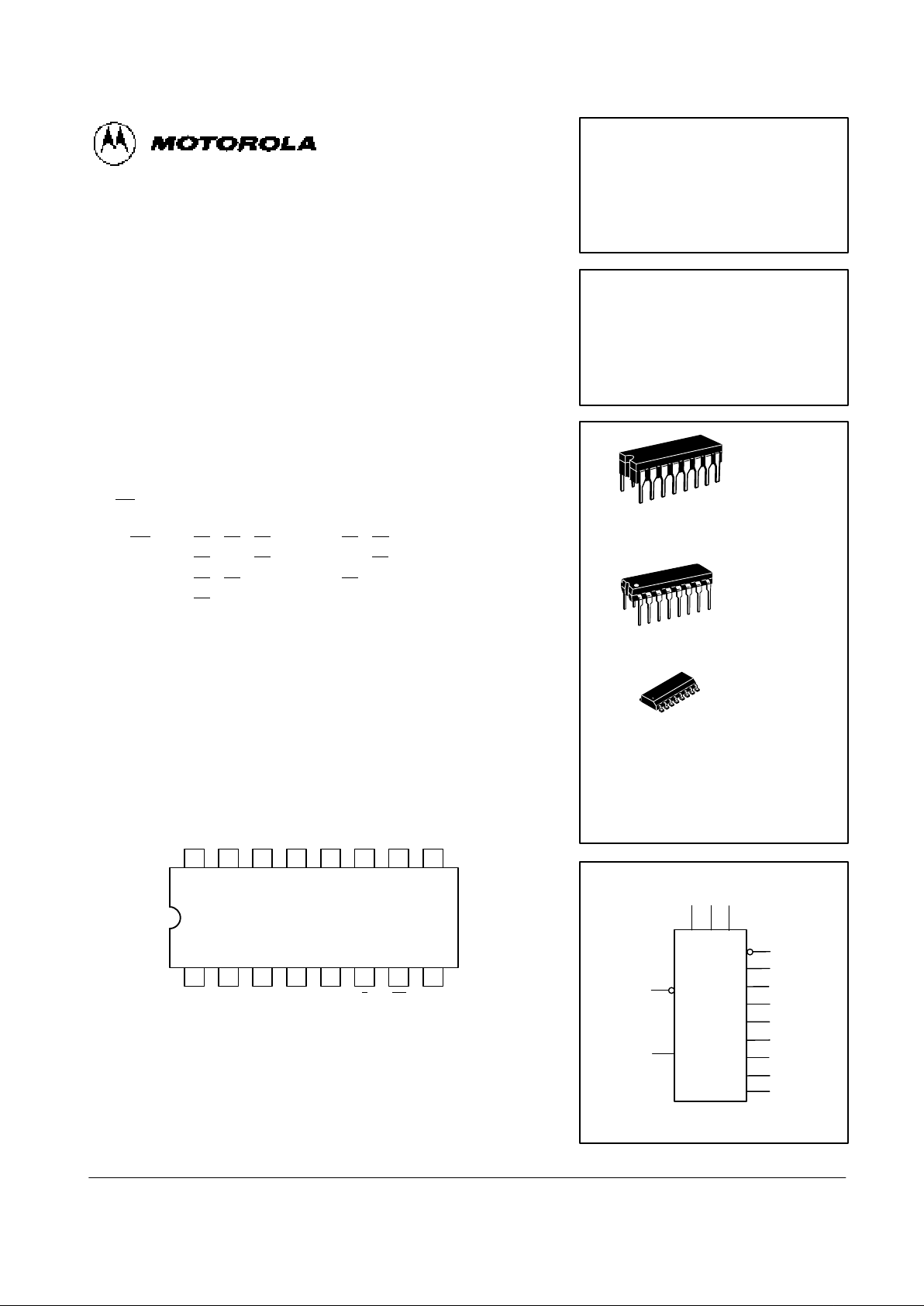
CONNECTION DIAGRAM
1516 14 13 12 11 10
21 3 4 5 6 7
V
CC
9
8
I
4
GND
I
5I6I7S0S1S2
I3I
2I1I0
Z Z
OE
FAST SCHOTTKY TTL
8-INPUT MULTIPLEXER
WITH 3-STATE OUTPUTS
MC54/74F251
J SUFFIX
CERAMIC
CASE 620-09
N SUFFIX
PLASTIC
CASE 648-08
16
1
16
1
ORDERING INFORMATION
MC54FXXXJ Ceramic
MC74FXXXN Plastic
MC74FXXXD SOIC
16
1
D SUFFIX
SOIC
CASE 751B-03
LOGIC SYMBOL
9 11
6
5
7
4
3
2
1
15
14
13
I
3
I
2
I
0
S
2
I
6
I
5
I
4
I
1
OE
VCC = PIN 16
GND = PIN 8
10
12
I
7
S1S
0
Page 2
4-118
FAST AND LS TTL DATA
MC54/74F251
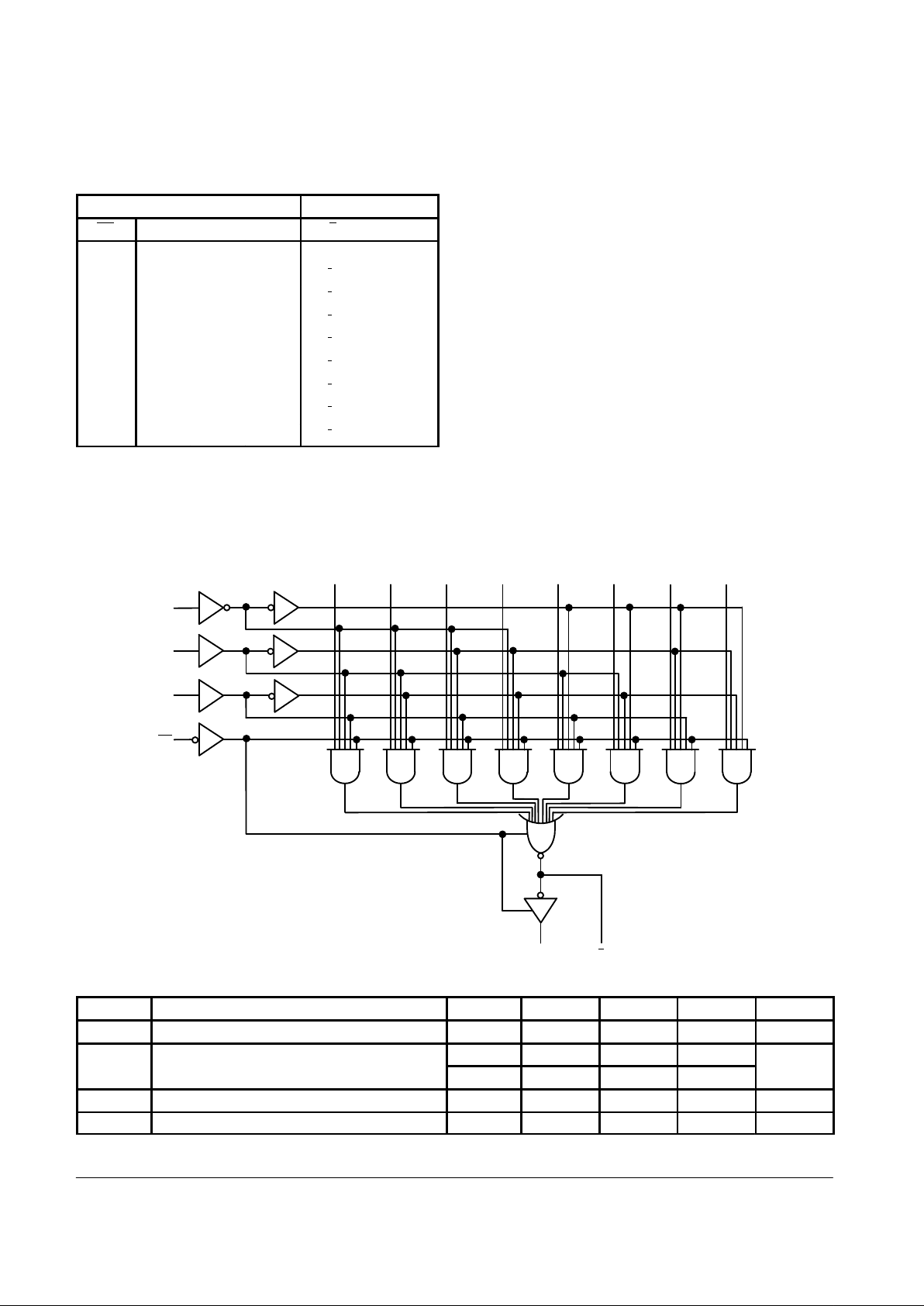
FUNCTION TABLE
Inputs Outputs
OE S
2
S
1
S
0
Z Z
H X X X Z Z
L L L L I
0
I
0
L L L H I
1
I
1
L L H L I
2
I
2
L L H H I
3
I
3
L H L L I
4
I
4
L H L H I
5
I
5
L H H L I
6
I
6
L H H H I
7
I
7
H = HIGH Voltage Level
L = LOW Voltage Level
X = Don’t Care
Z = High Impedance
LOGIC DIAGRAM
I
0
I
1
I
2
I
3
I
4
I
5
I
6
I
7
S
2
S
1
S
0
OE
Z Z
GUARANTEED OPERATING RANGES
Symbol Parameter Min Typ Max Unit
V
CC
Supply Voltage 54, 74 4.5 5.0 5.5 V
T
A
Operating Ambient Temperature Range 54 -55 25 125 °C
74 0 25 70
I
OH
Output Current — High 54, 74 –3.0 mA
I
OL
Output Current — Low 54, 74 24 mA
Page 3

4-119
FAST AND LS TTL DATA
MC54/74F251
DC CHARACTERISTICS OVER OPERATING TEMPERATURE RANGE (unless otherwise specified)
Limits
Symbol Parameter Min Typ Max Unit Test Conditions
V
IH
Input HIGH Voltage 2.0 V Guaranteed Input HIGH Voltage
V
IL
Input LOW Voltage 0.8 V Guaranteed Input LOW Voltage
V
IK
Input Clamp Diode Voltage –1.2 V IIN = –18 mA VCC = MIN
V
OH
Output HIGH Voltage 54, 74 2.4 3.4 V IOH = –3.0 mA VCC = 4.50 V
74 2.7 3.4 V IOH = –3.0 mA VCC = 4.75 V
V
OL
Output LOW Voltage 0.35 0.5 V IOL = 24 mA VCC = MIN
I
OZH
Output Off Current — HIGH 50 µA V
OUT
= 2.7 V VCC = MAX
I
OZL
Output Off Current — LOW –50 µA V
OUT
= 0.5 V VCC = MAX
I
IH
Input HIGH Current 20 µA VIN = 2.7 V VCC = MAX
100 µA VIN = 7.0 V
I
IL
Input LOW Current –0.6 mA VIN = 0.5 V VCC = MAX
I
OS
Output Short Circuit Current
(Note 2)
–60 –150 mA V
OUT
= 0 V VCC = MAX
I
CC
Power Supply Current 15 22 mA In, Sn = 4.5 V
OE
= GND VCC = MAX
16 24 OE, In = 4.5 V VCC = MAX
NOTES:
1. For conditions shown as MIN or MAX, use the appropriate value specified under guaranteed operating ranges.
2. Not more than one output should be shorted at a time, nor for more than 1 second.
AC CHARACTERISTICS
54/74F 54F 74F
TA = +25°C TA = -55 °Cto +125°C TA = 0°C to 70°C
VCC = +5.0 V VCC = 5.0 V ±10% VCC = 5.0 V ± 10%
CL = 50 pF CL = 50 pF CL = 50 pF
Symbol Parameter Min Max Min Max Min Max Unit
t
PLH
Propagation Delay 4.0 8.0 3.5 9.5 4.0 9.0 ns
t
PHL
Sn to Z
n
3.2 7.5 3.2 9.5 3.2 8.5
t
PLH
Propagation Delay 4.5 13 3.5 16.5 4.5 14 ns
t
PHL
Sn to Z
n
4.5 9.0 3.0 10.5 4.0 10.5
t
PLH
Propagation Delay 3.0 5.7 2.5 8.0 3.0 7.0 ns
t
PHL
In to Z 1.5 4.0 1.5 6.0 1.5 5.0
t
PLH
Propagation Delay 4.0 9.5 3.5 11.5 4.0 10.5 ns
t
PHL
In to Z 3.0 6.5 3.0 7.5 3.0 7.5
t
PZH
Output Enable Time 3.0 7.0 3.0 9.5 3.0 8.0 ns
t
PZL
OE to Z 3.0 8.5 3.0 10.5 3.0 9.5
t
PHZ
Output Disable Time 3.0 6.5 3.0 8.5 3.0 7.5 ns
t
PLZ
OE to Z 2.0 4.5 2.0 8.0 2.0 5.5
t
PZH
Output Enable Time 4.0 9.0 4.0 10 4.0 10 ns
t
PZL
OE to Z 3.5 8.0 3.5 10 3.5 9.0
t
PHZ
Output Disable Time 3.0 6.0 3.0 7.0 3.0 7.0 ns
t
PLZ
OE to Z 2.0 4.5 2.0 8.0 2.0 5.5
 Loading...