

Page 1
SEMICONDUCTOR TECHNICAL DATA
Motorola, Inc. 1996
1
2/96
REV 0
Ω
"
! ! !
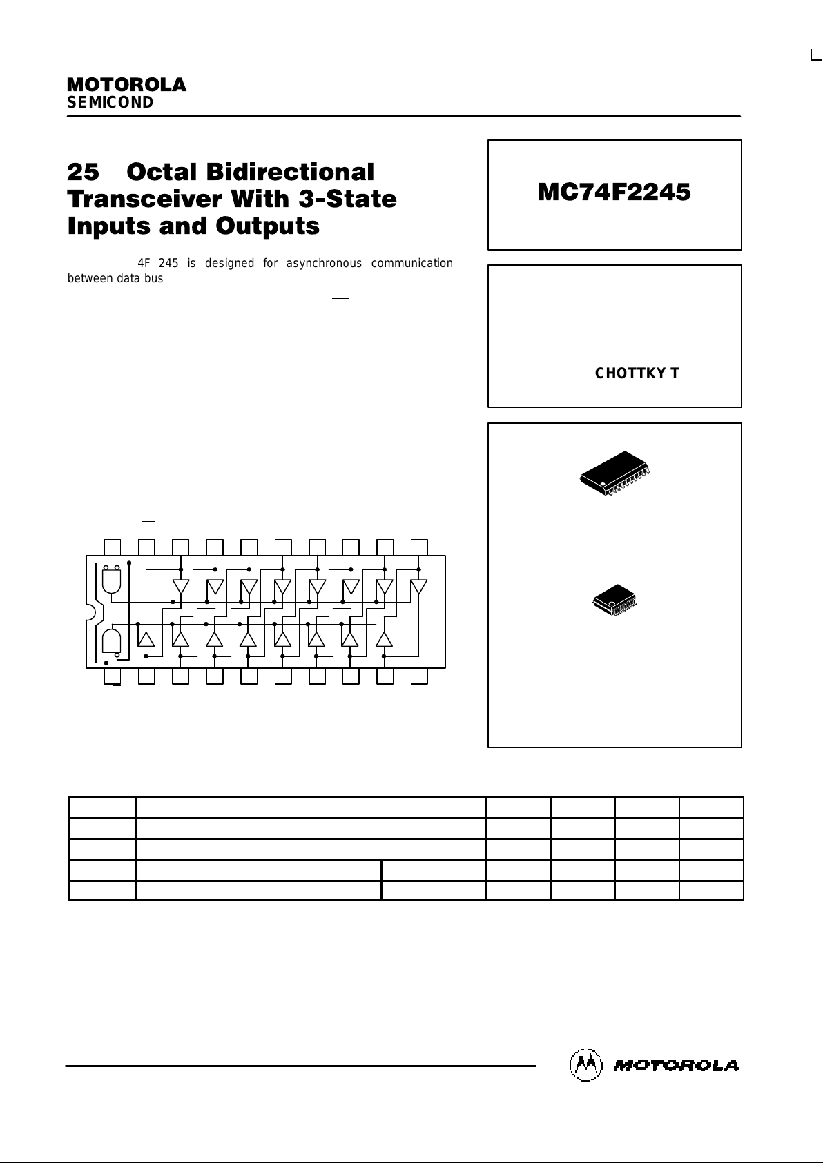
The MC74F2245 is designed for asynchronous communication
between data buses. The device transmits data from the A bus to the B
bus or from the B bus to the A bus depending upon the logic level at the
direction control (DIR) input. The output enable (OE
) input disables the
device so the buses are effectively isolated.
Both A and B outputs can sink up to 12mA; 25Ω resistors are included
in the lower output circuit to reduce overshoot and undershoot.
The MC74F2245 is characterized for operation from 0°C to 70°C.
• 3–State Outputs Drive Bus Lines or Buffer Memory Address Registers
• Package Options Include Plastic SOIC (DW–Suffix) and Plastic SSOP
(SD–Suffix)
111213141516171819
V
CC
1 2 3 4 5 6 7
20
OE B0B
1
B
2
B
4
B
3
A
1
T/R
A
0
A
2
A
3
A
5
A
4
CONNECTION DIAGRAM (TOP VIEW)
8 9 10
B
5
B
7
B
6
A
6
GNDA
7
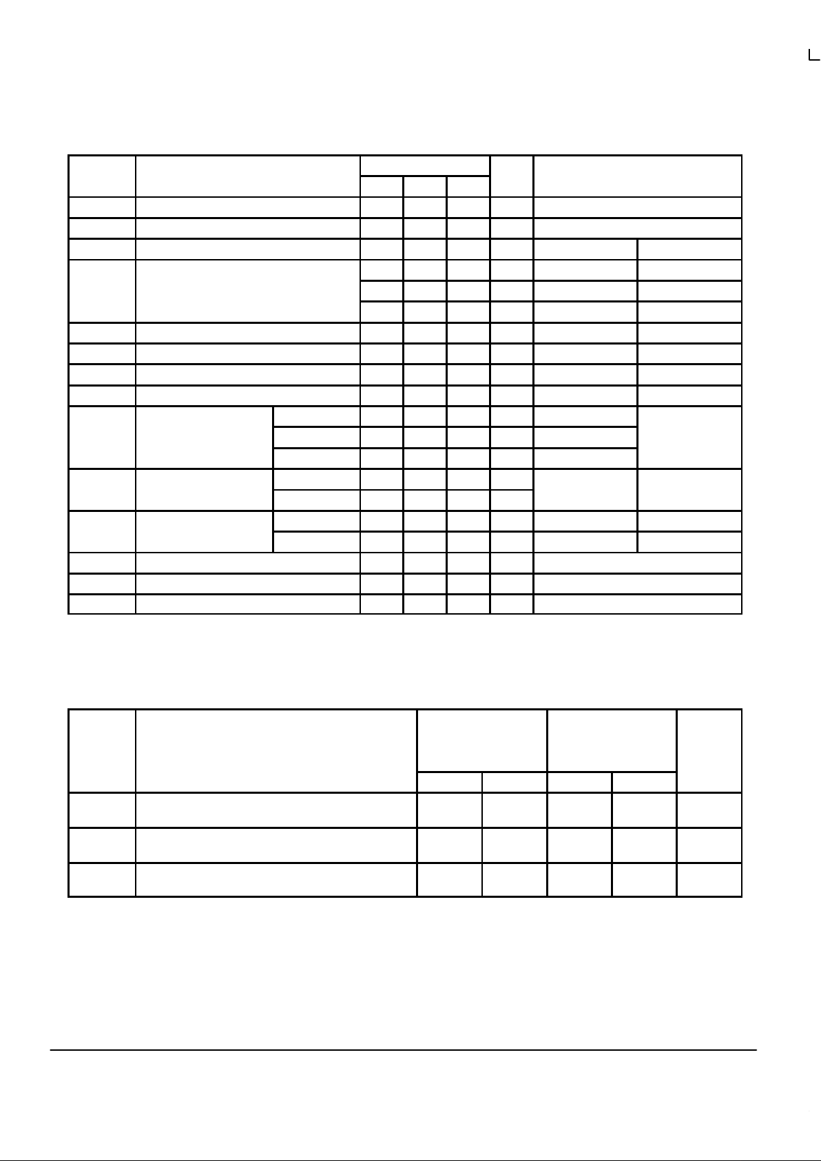
GUARANTEED OPERATING RANGES
Symbol Parameter Min Typ Max Unit
V
CC
Supply Voltage 4.5 5.0 5.5 V
T
A
Operating Ambient Temperature Range 0 25 70 °C
I
OH
Output Current — High Outputs –3.0 mA
I
OL
Output Current — Low Outputs 12 mA
25Ω OCTAL BIDIRECTIONAL
TRANSCEIVER WITH 3–STATE
INPUTS AND OUTPUTS
FAST SCHOTTKY TTL
DW SUFFIX
PLASTIC SOIC
CASE 751D–04
SD SUFFIX*
PLASTIC SSOP
CASE 940C–03
*Thermal Mounting Techniques are
Recommended. Please refer to Motorola
Application Note AN1567/D.
Page 2
MC74F2245
MOTOROLA TIMING SOLUTIONS
BR1333 — REV 5
2
DC CHARACTERISTICS OVER OPERATING TEMPERATURE RANGE (unless otherwise specified)
Limits
Symbol Parameter Min Typ Max Unit Test Conditions
V
IH
Input HIGH Voltage 2.0 V Guaranteed Input HIGH Voltage
V
IL
Input LOW Voltage 0.8 V Guaranteed Input LOW Voltage
V
IK
Input Clamp Diode Voltage –1.2 V IIN = –18 mA VCC = MIN
V
OH
Output HIGH Voltage, Outputs 2.5 V IOH = –1.0 mA VCC = 4.50 V
2.4 3.0 V IOH = –3.0 mA VCC = 4.50 V
2.7 3.2 V IOH = –3.0 mA VCC = 4.75 V
V
OL
Output LOW Voltage, Outputs 0.2 0.5 V IOL = 1 mA VCC = MIN
V
OL
Output LOW Voltage, Outputs 0.5 0.75 V IOL = 12 mA VCC = MIN
I
OZH
+ IIHOutput Off Current HIGH 70 µA V
OUT
= 2.7 V VCC = MAX
I
OZL
+ I
IL
Output Off Current LOW –650 mA V
OUT
= 0.5 V VCC = MAX
OE, T/R Inputs 20 µA VIN = 2.7 V
I
IH
Input HIGH Current OE, T/R Inputs 100 µA VIN = 7.0 V VCC = MAX
An, Bn Inputs 1.0 mA VIN = 5.5 V
T/R Input –0.8 mA
I
IL
Input LOW Current OE Input –1.2 mA VIN = 0.5 V VCC = MAX
I
OS
Output Short Circuit An Outputs –60 –150 mA V
OUT
= GND VCC = MAX
Current (Note 2) Bn Outputs –100 –225 mA V
OUT
= GND VCC = MAX
I
CCH
Power Supply Current HIGH 90 mA VCC = MAX, Outputs HIGH
I
CCL
Power Supply Current LOW 120 mA VCC = MAX, Outputs LOW
I
CCZ
Power Supply Current OFF 110 mA VCC = MAX, Outputs OFF
NOTES:
1. For conditions shown as MIN or MAX, use the appropriate value specified under recommended operating conditions for the applicable device type.
2. Not more than one output should be shorted at a time.
AC CHARACTERISTICS
TA = +25°C TA = 0°C to +70°C
VCC = +5.0 V VCC = 5.0 V ± 10%
CL = 50 pF CL = 50 pF
Symbol Parameter Min Max Min Max Unit
t
PLH
t
PHL
Propagation Delay
An to Bn or Bn to A
n
2.5
2.5
6.0
6.6
2.5
2.5
7.0
7.1
ns
t
PZH
t
PZL
Output Enable Time 3.0
3.5
7.3
10.6
3.0
3.5
8.5
12.0
ns
t
PHZ
t
PLZ
Output Disable Time 2.5
2.0
6.5
6.5
2.5
2.0
7.5
7.5
ns
Page 3

MC74F2245
TIMING SOLUTIONS
BR1333 — REV 5
3 MOTOROLA
WAVEFORM 1 – PROPAGATION DELAYS
tR = tF = 2.5ns, 10% to 90%; f = 1MHz; tW = 500ns
3.0V
0V
V
OH
V
OL
An, Bn
Bn, An
t
PHL
t
PLH
WAVEFORM 2 – OUTPUT ENABLE AND DISABLE TIMES
tR = tF = 2.5ns, 10% to 90%; f = 1MHz; tW = 500ns
3.0V
0V
≈
0V
OE
, T/R
An, Bn
t
PZH
≈
3.5V
t
PHZ
t
PZL
t
PLZ
An, Bn
1.5V
1.5V
1.5V1.5V
1.5V 1.5V
Figure 1. AC Waveforms
1.5V
V
OH
VOH – 0.3V
VOL + 0.3V
GND
1.5V
OPEN
PULSE
GENERATOR
R
T
DUT
V
CC
R
L
R
1
C
L
7V
TEST SWITCH
t
PLH
, t
PHL
Open
t
PZL
, t
PLZ
7V
t
PZH
, t
PHZ
Open
CL = 50pF or equivalent (Includes jig and probe capacitance)
RL = R1 = 500Ω or equivalent
RT = Z
OUT
of pulse generator (typically 50Ω)
Figure 2. Test Circuit
Page 4

MC74F2245
MOTOROLA TIMING SOLUTIONS
BR1333 — REV 5
4
OUTLINE DIMENSIONS
SD SUFFIX
PLASTIC SSOP PACKAGE
CASE 940C–03
ISSUE B
20 11
101
H
A
B
F
M
K20X REF
S
U
M
0.12 (0.005) V
S
T
L
L/2
PIN 1
IDENT
S
U
M
0.20 (0.008) T
–V–
–U–
D
C
0.076 (0.003)
G
–T–
SEATING
PLANE
DETAIL E
N
N
0.25 (0.010)
K
J
J1
K1
SECTION N–N
DIMAMIN MAX MIN MAX
INCHES
7.07 7.33 0.278 0.288
MILLIMETERS
B 5.20 5.38 0.205 0.212
C 1.73 1.99 0.068 0.078
D 0.05 0.21 0.002 0.008
F 0.63 0.95 0.024 0.037
G 0.65 BSC 0.026 BSC
H 0.59 0.75 0.023 0.030
J 0.09 0.20 0.003 0.008
J1 0.09 0.16 0.003 0.006
K 0.25 0.38 0.010 0.015
K1 0.25 0.33 0.010 0.013
_ _ _ _
NOTES:
1. DIMENSIONING AND TOLERANCING PER ANSI
Y14.5M, 1982.
2. CONTROLLING DIMENSION: MILLIMETER.
3. DIMENSION A DOES NOT INCLUDE MOLD FLASH,
PROTRUSIONS OR GATE BURRS. MOLD FLASH
OR GATE BURRS SHALL NOT EXCEED 0.15
(0.006) PER SIDE.
4. DIMENSION B DOES NOT INCLUDE INTERLEAD
FLASH OR PROTRUSION. INTERLEAD FLASH OR
PROTRUSION SHALL NOT EXCEED 0.15 (0.006)
PER SIDE.
5. DIMENSION K DOES NOT INCLUDE DAMBAR
PROTRUSION/INTRUSION. ALLOWABLE DAMBAR
PROTRUSION SHALL BE 0.13 (0.005) TOTAL IN
EXCESS OF K DIMENSION AT MAXIMUM
MATERIAL CONDITION. DAMBAR INTRUSION
SHALL NOT REDUCE DIMENSION K BY MORE
THAN 0.07 (0.002) AT LEAST MATERIAL
CONDITION.
6. TERMINAL NUMBERS ARE SHOWN FOR
REFERENCE ONLY.
7. DIMENSION A AND B ARE TO BE DETERMINED
AT DATUM PLANE –W–.
L 7.65 7.90 0.301 0.311
M 0 8 0 8
DETAIL E
–W–
Page 5

MC74F2245
TIMING SOLUTIONS
BR1333 — REV 5
5 MOTOROLA
OUTLINE DIMENSIONS
DW SUFFIX
PLASTIC SOIC PACKAGE
CASE 751D–04
ISSUE E
NOTES:
1. DIMENSIONING AND TOLERANCING PER
ANSI Y14.5M, 1982.
2. CONTROLLING DIMENSION: MILLIMETER.
3. DIMENSIONS A AND B DO NOT INCLUDE
MOLD PROTRUSION.
4. MAXIMUM MOLD PROTRUSION 0.150
(0.006) PER SIDE.
5. DIMENSION D DOES NOT INCLUDE
DAMBAR PROTRUSION. ALLOWABLE
DAMBAR PROTRUSION SHALL BE 0.13
(0.005) TOTAL IN EXCESS OF D DIMENSION
AT MAXIMUM MATERIAL CONDITION.
–A–
–B–
20
1
11
10
S
A
M
0.010 (0.25) B
S
T
D20X
M
B
M
0.010 (0.25)
P10X
J
F
G
18X
K
C
–T–
SEATING
PLANE
M
R
X 45
_
DIM MIN MAX MIN MAX
INCHESMILLIMETERS
A 12.65 12.95 0.499 0.510
B 7.40 7.60 0.292 0.299
C 2.35 2.65 0.093 0.104
D 0.35 0.49 0.014 0.019
F 0.50 0.90 0.020 0.035
G 1.27 BSC 0.050 BSC
J 0.25 0.32 0.010 0.012
K 0.10 0.25 0.004 0.009
M 0 7 0 7
P 10.05 10.55 0.395 0.415
R 0.25 0.75 0.010 0.029
_ _
_ _
How to reach us:
USA/EUROPE: Motorola Literature Distribution; JAPAN: Nippon Motorola Ltd.; Tatsumi–SPD–JLDC, Toshikatsu Otsuki,
P.O. Box 20912; Phoenix, Arizona 85036. 1–800–441–2447 6F Seibu–Butsuryu–Center, 3–14–2 Tatsumi Koto–Ku, Tokyo 135, Japan. 03–3521–8315
MFAX: RMFAX0@email.sps.mot.com –TOUCHTONE (602) 244–6609 HONG KONG: Motorola Semiconductors H.K. Ltd.; 8B Tai Ping Industrial Park,
INTERNET: http://Design–NET.com 51 Ting Kok Road, Tai Po, N.T., Hong Kong. 852–26629298
Motorola reserves the right to make changes without further notice to any products herein. Motorola makes no warranty , representation or guarantee regarding
the suitability of its products for any particular purpose, nor does Motorola assume any liability arising out of the application or use of any product or circuit,
and specifically disclaims any and all liability, including without limitation consequential or incidental damages. “T ypical” parameters can and do vary in different
applications. All operating parameters, including “T ypicals” must be validated for each customer application by customer’s technical experts. Motorola does
not convey any license under its patent rights nor the rights of others. Motorola products are not designed, intended, or authorized for use as components in
systems intended for surgical implant into the body, or other applications intended to support or sustain life, or for any other application in which the failure of
the Motorola product could create a situation where personal injury or death may occur. Should Buyer purchase or use Motorola products for any such
unintended or unauthorized application, Buyer shall indemnify and hold Motorola and its officers, employees, subsidiaries, affiliates, and distributors harmless
against all claims, costs, damages, and expenses, and reasonable attorney fees arising out of, directly or indirectly, any claim of personal injury or death
associated with such unintended or unauthorized use, even if such claim alleges that Motorola was negligent regarding the design or manufacture of the part.
Motorola and are registered trademarks of Motorola, Inc. Motorola, Inc. is an Equal Opportunity/Affirmative Action Employer.
MC74F2245/D
*MC74F2245/D*
◊
 Loading...