

Page 1
4-97
FAST AND LS TTL DATA
CARRY LOOKAHEAD
GENERATOR
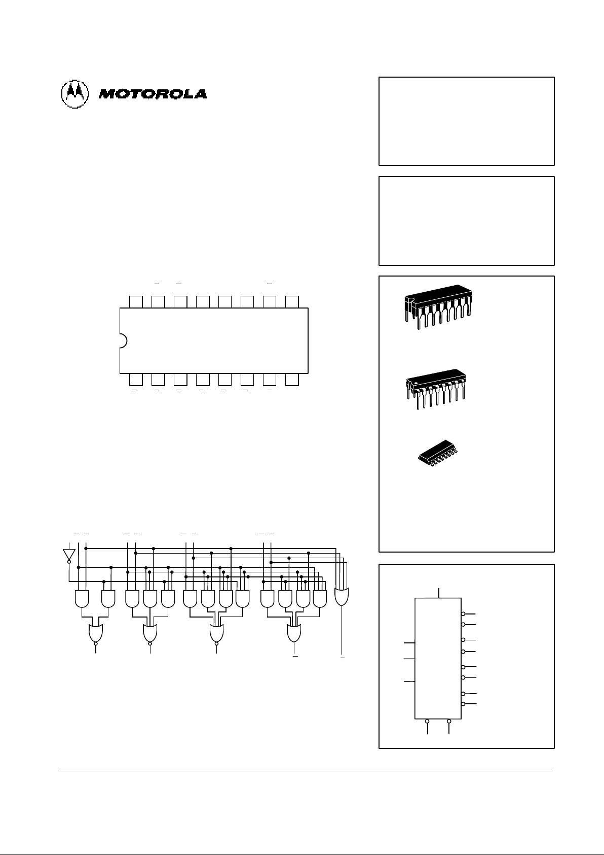
The MC54/74F182 is a high-speed carry lookahead generator. It is generally used with the F181, F381 or 29F01 4-bit arithmetic logic unit to provide highspeed lookahead over word lengths of more than four bits.
• Provides Lookahead Carries Across a Group of Four ALUs
• Multi-level Lookahead High-speed Arithmetic Operation Over Long
Word Lengths
Cn +
x
CONNECTION DIAGRAM DIP (TOP VIEW)
1516 14 13 12 11 10
21 3 4 5 6 7
V
CC
9
8
P
2G2Cn
Cn + yG
Cn +
z
G
1P1G0P0G3P3
P
GND
LOGIC DIAGRAM
Cn +
x
G
3
G
P
3
G2P
2
G
1P1
G
0P0
C
n
Cn +
y
Cn +
z
P
MC54FXXXJ Ceramic
MC74FXXXN Plastic
MC74FXXXD SOIC
MC54/74F182
CARRY LOOKAHEAD
GENERATOR
FAST SCHOTTKY TTL
J SUFFIX
CERAMIC
CASE 620-09
N SUFFIX
PLASTIC
CASE 648-08
16
1
16
1
ORDERING INFORMATION
16
1
D SUFFIX
SOIC
CASE 751B-03
LOGIC SYMBOL
13
4
3
2
1
15
14
6
5
7 10
9
11
12
C
n
P
0
G
0
P
1
G
1
P
2
G
2
P
3
G
3
P G
Cn +
x
Cn +
y
Cn +
z
VCC = PIN 16
GND = PIN 8
Page 2
4-98
FAST AND LS TTL DATA
MC54/74F182
FUNCTION TABLE
Inputs Outputs
C
n
G
0
P
0
G
1
P
1
G
2
P
2
G
3
P
3
C
n+x
C
n+y
C
n+z
G P
X H H L
L H X L
X L X H
H X L H
X X X H H L
X H H H X L
L H X H X L
X X X L X H
X L X X L H
H X L X L H
X X X X X H H L
X X X H H H X L
X H H H X H X L
L H X H X H X L
X X X X X L X H
X X X L X X L H
X L X X L X L H
H X L X L X L H
X X X X X H H H
X X X H H H X H
X H H H X H X H
H H X H X H X H
X X X X X L X L
X X X L X X L L
X L X X L X L L
L X L X L X L L
H X X X H
X H X X H
X X H X H
X X X H H
L L L L L
H = HIGH Voltage Level
L = LOW Voltage Level
X = Don’t Care
GUARANTEED OPERATING RANGES
Symbol Parameter Min Typ Max Unit
V
CC
Supply Voltage 54,74 4.5 5.0 5.5 V
T
A
Operating Ambient Temperature Range
54 –55 25 125 °C
A
74 0 25 70
I
OH
Output Current — High 54, 74 –1.0 mA
I
OL
Output Current — Low 54, 74 20 mA
Page 3

4-99
FAST AND LS TTL DATA
MC54/74F182
DC CHARACTERISTICS OVER OPERATING TEMPERATURE RANGE (unless otherwise specified)
Limits
Symbol Parameter Min Typ Max Unit Test Conditions
V
IH
Input HIGH Voltage 2.0 V Guaranteed Input HIGH Voltage
V
IL
Input LOW Voltage 0.8 V Guaranteed Input LOW Voltage
V
IK
Input Clamp Diode Voltage –1.2 V IIN = –18 mA VCC = MIN
V
OH
Output HIGH Voltage 54, 74 2.5 3.4 V IOH = –1.0 mA VCC = 4.50 V
74 2.7 3.4 V IOH = –1.0 mA VCC = 4.75 V
V
OL
Output LOW Voltage 0.35 0.5 V IOL = 20 mA VCC = MIN
I
IH
Input HIGH Current 20 µA VIN = 2.7 V VCC = MAX
100 µA VIN = 7.0 V VCC = MAX
Cn Input –1.2
P
3
Input
–2.4
I
IL
Input LOW P
2
Input
–3.6 mA VIN = 0.5 V VCC = MAX
Current G
3
, P0, P1 Inputs
–4.8
G
0
, G2 Inputs
–8.4
G
1
Input
–9.6
I
OS
Output Short Circuit Current (Note 2) –60 –150 mA V
OUT
= 0 V VCC = MAX
I
CCH
Power Supply Current (All Outputs HIGH) 18.4 28 mA P
3
, G3 = 4.5 V
All Other Inputs = GND
VCC = MAX
I
CCL
Power Supply Current (All Outputs LOW) 23.5 36 mA G
0
, G1, G2 = 4.5 V
All Other Inputs = GND
VCC = MAX
NOTES:
1. For conditions shown as MIN or MAX, use the appropriate value specified under guaranteed operating ranges.
2. No more than one output should be shorted at a time, nor for more than 1 second.
AC CHARACTERISTICS
54/74F 54F 74F
TA = +25°C TA = –55°C to +125°C TA = 0°C to +70°C
VCC = +5.0 V VCC = 5.0 V ± 10% VCC = 5.0V ± 10%
CL = 50 pF CL = 50 pF CL = 50 pF
Symbol Parameter Min Typ Max Min Max Min Max Unit
t
PLH
Propagation Delay 3.0 6.6 8.5 3.0 10.5 3.0 9.5
t
PHL
Cn to Cn + x, Cn + y, Cn +
z
3.0 6.8 9.0 3.0 11 3.0 10
ns
t
PLH
Propagation Delay 2.5 6.2 8.0 2.5 10.7 2.5 9.0
t
PHL
P
0
, P1, or P2 to Cn + x,
Cn + y, Cn +
z
1.5 3.7 5.0 1.5 6.5 1.5 6.0
ns
t
PLH
Propagation Delay 2.5 6.5 8.5 2.5 10.5 2.5 9.5
t
PHL
G
0
, G1, or G2 to Cn + x,
Cn + y, Cn +
z
1.5 3.9 5.2 1.5 6.5 1.5 6.0
ns
Page 4

4-100
FAST AND LS TTL DATA
MC54/74F182
AC CHARACTERISTICS (Continued)
54/74F 54F 74F
TA = +25°C TA = –55°C to +125°C TA = 0°C to +70°C
VCC = +5.0 V VCC = 5.0 V ± 10% VCC = 5.0V ± 10%
CL = 50 pF CL = 50 pF CL = 50 pF
Symbol Parameter Min Typ Max Min Max Min Max Unit
t
PLH
Propagation Delay 2.0 7.9 10 2.0 12.5 2.0 11
t
PHL
P
1
, P2, or P3 to G
2.0 6.0 8.0 2.0 9.5 2.0 9.0
ns
t
PLH
Propagation Delay 2.0 8.3 10.5 2.0 12.5 2.0 11.5
t
PHL
G
n
to G
1.5 5.7 7.5 1.5 9.5 1.5 8.5
ns
t
PLH
Propagation Delay 2.5 5.7 7.5 2.5 11 2.5 8.5
t
PHL
P
n
to P
2.5 4.1 5.5 2.5 7.5 2.5 6.5
ns
FUNCTIONAL DESCRIPTION
The F182 carry lookahead generator accepts up to four
pairs of active-LOW Carry Propagate (P0-P3) and carry Generate (G
0-G3
) signals and an active-HIGH Carry input (Cn) and
provides anticipated active-HIGH carries (Cn + x, Cn + y, Cn + z)
across four groups of binary adders. The F182 also has active-LOW Carry Propagate (P
) and Carry Generate (G) outputs which may be used for further levels of lookahead. The
logic equations provided at the output are:
Cn + x = G0 + P0C
n
Cn + y = G1 + P1G0 + P1P0C
n
Cn + z = G2 + P2G1 + P2P1G0 + P2P1P0C
n
G = G
3
+ P3G2 + P3P2G1 + P3P2P1G
0
P = P3P2P1P
0
Also, the F182 can be used with binary ALUs in an activeLOW or active-HIGH input operand mode. The connections
(Figure 1) to and from the ALU to the carry lookahead generator are identical in both cases. Carries are rippled between
lookahead blocks. The critical speed path follows the circled
numbers. There are several possible arrangements for the
carry interconnects, but all achieve about the same speed. A
28-bit ALU is formed by dropping the last F181 or F381.
5
3
2
1
Figure 1. 32-Bit ALU with Ripple Carry Between 16-Bit Lookahead ALUs
Cn
ALU**
G
P
Cn
ALU**
G
P
Cn
ALU**
G
P
Cn
ALU**
G
P
A
, B
C
n
Cn +
4
ALU**
G
P
C
n
Cn +
4
ALU**
G
P
CnCn +
4
ALU**
C
n
Cn +
4
ALU**
C
OUT
(C
32)
F
C
IN
P0G
0
P1G1P
2
G
2
P3G
3
G
P
C
n
Cn + xCn + yCn +
z
F182
P0G0P1G1P2G2P3G
3
G
P
C
n
Cn + xCn + yCn +
z
F182
C
16
** ALUs may be either F181, F381, or 2901A.
6
4
 Loading...