

Datasheet MC74F161AD, MC74F161AN, MC74F163AN, MC54F163AJ, MC54F161AJ Datasheet (Motorola)
...Page 1
4-75
FAST AND LS TTL DATA
SYNCHRONOUS PRESETTABLE
BINARY COUNTER
The MC74F161A and MC74F163A are high-speed synchronous modulo-16 binary counters. They are synchronously presettable for application in
programmable dividers and have two types of Count Enable inputs plus a T erminal Count output for versatility in forming synchronous multistage counters.
The MC74F161A has an asynchronous Master Reset input that overrides all
other inputs and forces the outputs LOW. The MC74F163A has a Synchronous Reset input that overrides counting and parallel loading and allows the
outputs to be simultaneously reset on the rising edge of the clock.
• Synchronous Counting and Loading
• High-Speed Synchronous Expansion
• Typical Count Frequency of 120 MHz
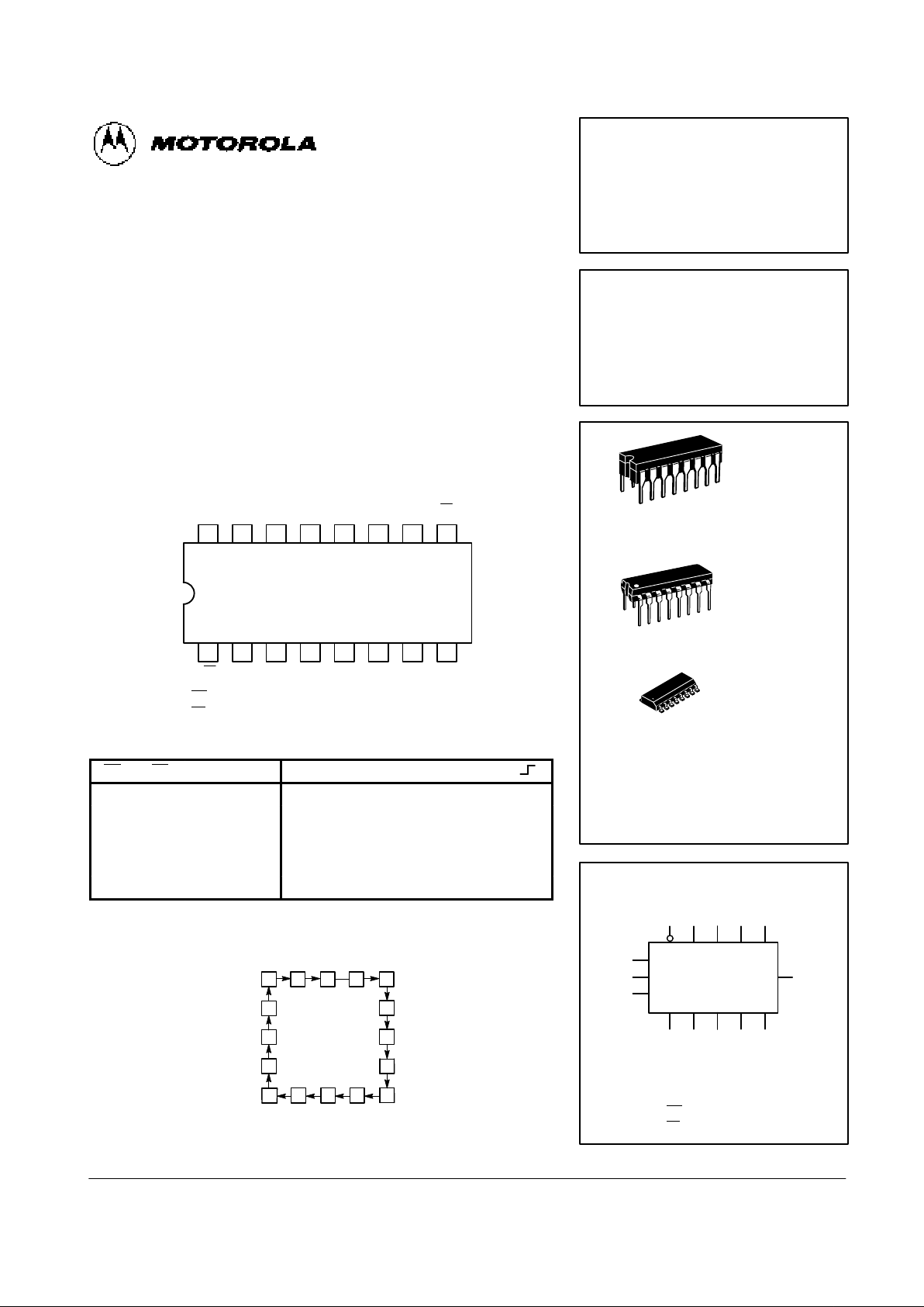
CONNECTION DIAGRAM
1516 14 13 12 11 10
21 3 4 5 6 7
V
CC
9
8
TC Q0Q1Q2Q3CET PE
*R CP P0P1P2P3CEP GND
*MR for MC74F161A
*SR for MC74F163A
FUNCTION TABLE
SR PE CET CEP ACTION ON THE RISING CLOCK EDGE ( )
L X X X Reset (Clear)
H L X X Load (Pn º Qn)
H H H H Count (Increment)
H H L X No Change (Hold)
H H X L No Change (Hold)
H = HIGH Voltage Level; L = LOW Voltage Level; X = Don’t Care
STATE DIAGRAM
15
12
1 2 3 4
5
6
7
8
91011
13
14
0
VCC = PIN 16
GND = PIN 8
LOGIC SYMBOL
PE P
0
P
1
P3P
2
CEP
CET
CP
*R
Q
0
Q
1
Q2Q
3
TC
1
15
7
14 13 12 11
9 3 4 5 6
10
2
MC74F161A
MC74F163A
SYNCHRONOUS PRESETTABLE
BINARY COUNTER
FAST SHOTTKY TTL
J SUFFIX
CERAMIC
CASE 620-09
N SUFFIX
PLASTIC
CASE 648-08
16
1
16
1
ORDERING INFORMATION
MC74FXXXAJ Ceramic
MC74FXXXAN Plastic
MC74FXXXAD SOIC
16
1
D SUFFIX
SOIC
CASE 751B-03
*MR for MC74F161A
*SR
for MC74F163A
Page 2
4-76
FAST AND LS TTL DATA
MC74F161A • MC74F163A
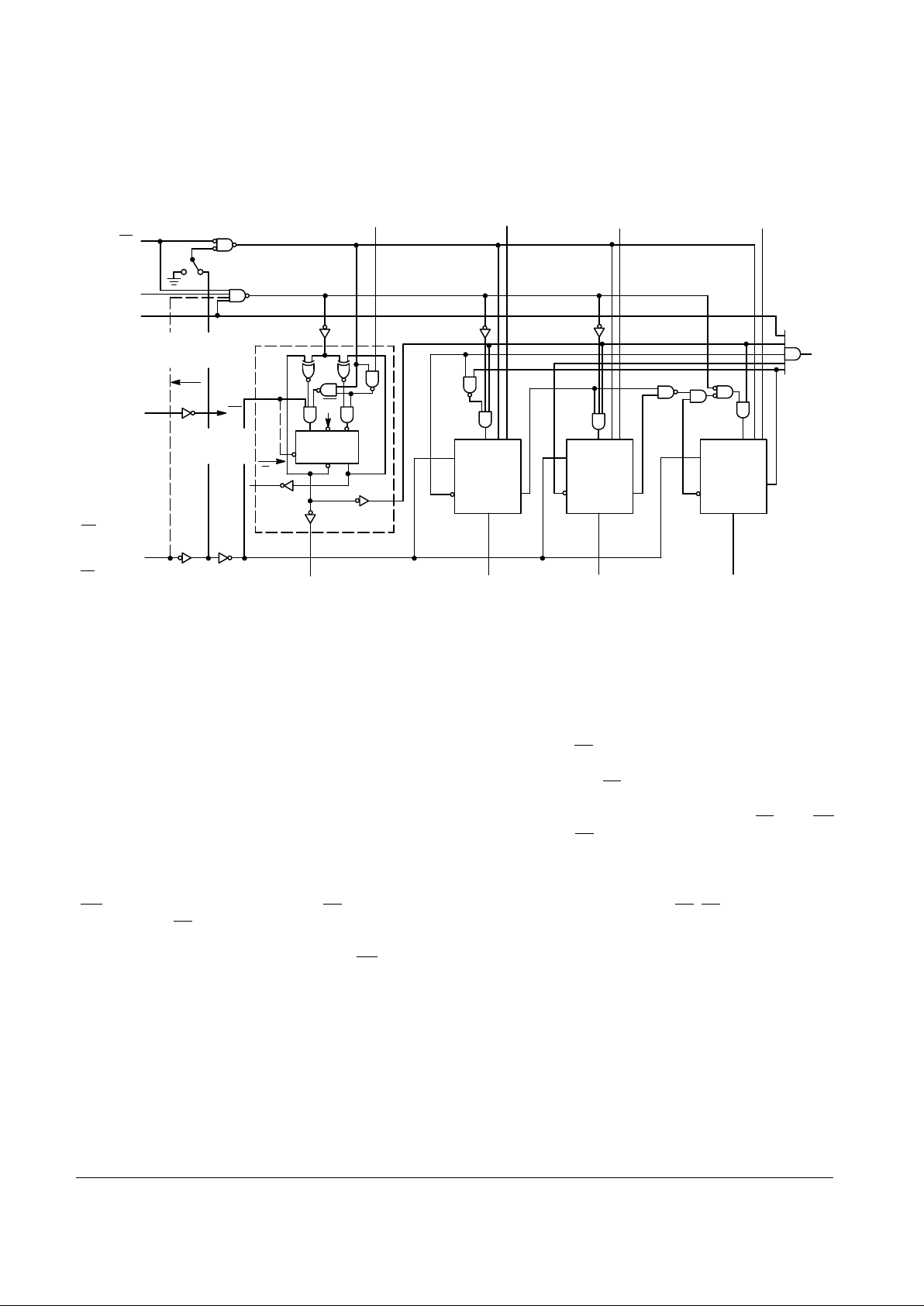
CP
D
NOTE:
This diagram is provided only for the understanding of logic operations and should not be used to estimate propagation delays.
LOGIC DIAGRAM
DETAIL A DETAIL A
DETAIL A
DETAIL A
P
0
P
1
P
3
P
2
CEP
CET
CP
Q
0
Q
1
Q
2
Q
3
MR
(MC74F161A)
SR
(MC74F163A)
Q
0
Q
0
TC
CP
CP D
Q Q
C
D
MC74F161A
MC74F163A
MC74F163A
ONLY
MC74F161A
ONLY
PE
FUNCTIONAL DESCRIPTION
The MC74F161A and MC74F163A count in modulo-16
binary sequence. From state 15 (HHHH) they increment to
state 0 (LLLL). The clock inputs of all flip-flops are driven in
parallel through a clock buffer. Thus all changes of the Q outputs (except due to Master Reset of the MC74F161A) occur
as a result of, and synchronous with, the LOW-to-HIGH transition of the CP input signal. The circuits have four fundamental
modes of operation, in order of precedence: asynchronous reset (MC74F161A), synchronous reset (MC74F163A), parallel
load, count-up and hold. Five control inputs Master Reset
(MR
, MC74F161A), Synchronous Reset (SR, MC74F163A),
Parallel Enable (PE
), Count Enable Parallel (CEP) and Count
Enable Trickle (CET) — determine the mode of operation, as
shown in the Function Table. A LOW signal on MR
overrides
all other inputs and asynchronously forces all outputs LOW. A
LOW signal on SR
overrides counting and parallel loading
and allows all outputs to go LOW on the next rising edge of
CP. A LOW signal on PE
overrides counting and allows information on the Parallel Data (Pn) inputs to be loaded into the
flip-flops on the next rising edge of CP. With PE
and MR
(MC74F161A) or SR (MC74F163A) HIGH, CEP and CET permit counting when both are HIGH. Conversely , a LOW signal
on either CEP or CET inhibits counting.
The MC74F161A and MC74F163A use D-type edge-trig-
gered flip-flops and changing the SR
, PE, CEP, and CET inputs when the CP is in either state does not cause errors, provided that the recommended setup and hold times, with
respect to the rising edge of CP, are observed.
Page 3

4-77
FAST AND LS TTL DATA
MC74F161A • MC74F163A
GUARANTEED OPERATING RANGES
Symbol Parameter Min Typ Max Unit
V
CC
Supply Voltage 74 4.5 5.0 5.5 V
T
A
Operating Ambient Temperature Range 74 0 25 70 °C
I
OH
Output Current — High 74 – 1.0 mA
I
OL
Output Current — Low 74 20 mA
DC CHARACTERISTICS OVER OPERATING TEMPERATURE RANGE (unless otherwise specified)
Limits
Symbol Parameter Min Typ Max Unit Test Conditions
V
IH
Input HIGH Voltage 2.0 V Guaranteed Input HIGH Voltage for
All Inputs
V
IL
Input LOW Voltage 0.8 V Guaranteed Input LOW Voltage for
All Inputs
V
IK
Input Clamp Diode Voltage –1.2 V VCC = MIN, IIN = – 18 mA
V
OH
Output HIGH Voltage 74 2.5 3.4 V IOH = –1.0 mA VCC = 4.50 V
74 2.7 3.4 V IOH = –1.0 mA VCC = 4.75 V
V
OL
Output LOW Voltage 0.35 0.5 V IOL = 20 mA VCC = MIN
I
IH
Input HIGH Current 20 µA VCC = MAX, VIN = 2.7 V
0.1 mA VCC = MAX, VIN = 7.0 V
I
IL
Input LOW Current
Data, CEP, Clock
PE
, CET, SR
–0.6
–1.2
mA VCC = MAX, VIN = 0.5 V
I
OS
Output Short Circuit Current (Note 2) –60 – 150 mA VCC = MAX, V
OUT
= 0 V
I
CC
Power Supply Current 37 55 mA VCC = MAX
NOTES:
1. For conditions shown as MIN or MAX, use the appropriate value specified under recommended operating conditions for the applicable device type.
2. Not more than one output should be shorted at a time, nor for more than 1 second.
The T erminal Count (TC) output is HIGH when CET is HIGH
and the counter is in state 15. T o implement synchronous multistage counters, the TC outputs can be used with the CEP
and CET inputs in two different ways. The TC output is subject
to decoding spikes due to internal race conditions and is there-
fore not recommended for use as a clock or asynchronous
reset for flip-flops, counters, or registers.
Logic Equations:
Count Enable = CEP • CET • PE
TC = Q0 • Q1 • Q2 • Q3 • CET
Page 4

4-78
FAST AND LS TTL DATA
MC74F161A • MC74F163A
AC CHARACTERISTCS
74F 74F
TA = +25°C TA = 0°C to 70°C
VCC = +5.0 V VCC = 5.0 V ± 10%
CL = 50 pF CL = 50 pF
Symbol Parameter Min Max Min Max Unit
f
max
Maximum Count Frequency 100 90 MHz
t
PLH
Propagation Delay, Count 3.5 6.0 3.5 7.0
t
PHL
CP to Qn (PE Input HIGH) 3.5 10 3.5 11 ns
t
PLH
Propagation Delay 3.5 7.0 3.5 9.5
t
PHL
CP to Qn (PE Input LOW) 4.0 8.5 4.0 9.5
t
PLH
Propagation Delay 5.0 14 5.0 15 ns
t
PHL
CP to TC 4.5 14 4.5 15
t
PLH
Propagation Delay 2.5 7.5 2.5 8.5 ns
t
PHL
CET to TC 2.5 7.5 2.5 8.5
t
PHL
Propagation Delay
MR
to Qn (MC74F161A)
5.5 12 5.5 13 ns
t
PHL
Propagation Delay
MR
to TC (MC74F161A)
4.5 10.5 4.5 11.5 ns
AC OPERATING REQUIREMENTS
74F 74F
TA = +25°C TA = 0°C to 70°C
VCC = +5.0 V VCC = 5.0 V ± 10%
CL = 50 pF CL = 50 pF
Symbol Parameter Min Max Min Max Unit
ts(H) Setup Time, HIGH or LOW 5.0 5.0
ts(L) Pn to CP 5.0 5.0 ns
th(H) Hold Time, HIGH or LOW 2.0 2.0
th(L) Pn to CP 2.0 2.0
ts(H) Setup Time, HIGH or LOW 11 11.5
ts(L) PE or SR to CP 8.5 9.5 ns
th(H) Hold Time, HIGH or LOW 2.0 2.0
th(L) PE or SR to CP 0 0
ts(H) Setup Time, HIGH or LOW 11 11.5
ts(L) CEP or CET to CP 5.0 5.0 ns
th(H) Hold Time, HIGH or LOW 0 0
th(L) CEP or CET to CP 0 0
tw(H) Clock Pulse Width (Load) 5.0 5.0 ns
tw(L) HIGH or LOW 5.0 5.0
tw(H) Clock Pulse Width (Count) 4.0 4.0 ns
tw(L) HIGH or LOW 6.0 7.0
tw(L) MR Pulse Width, LOW
(MC74F161A)
5.0 5.0
ns
t
rec
Recovery Time, MR to CP (MC74F161A) 6.0 6.0
 Loading...