

Page 1
5-1
FACT DATA
The MC74AC350/74ACT350 is a specialized multiplexer that accepts a 4-bit
word and shifts it 0, 1, 2 or 3 places, as determined by two Select (S0, S1) inputs.
For expansion to longer words, three linking inputs are provided for lower-order
bits; thus two packages can shift an 8-bit word, four packages a 16-bit word, etc.
Shifting by more than three places is accomplished by paralleling the 3-state outputs
of different packages and using the Output Enable (OE
) inputs as a third Select
level. With appropriate interconnections, the ′AC/ACT350 can perform zero-backfill,
sign-extend or end-around (barrel) shift functions.
• Linking Inputs for Word Expansion
• 3-State Outputs for Extending Shift Range
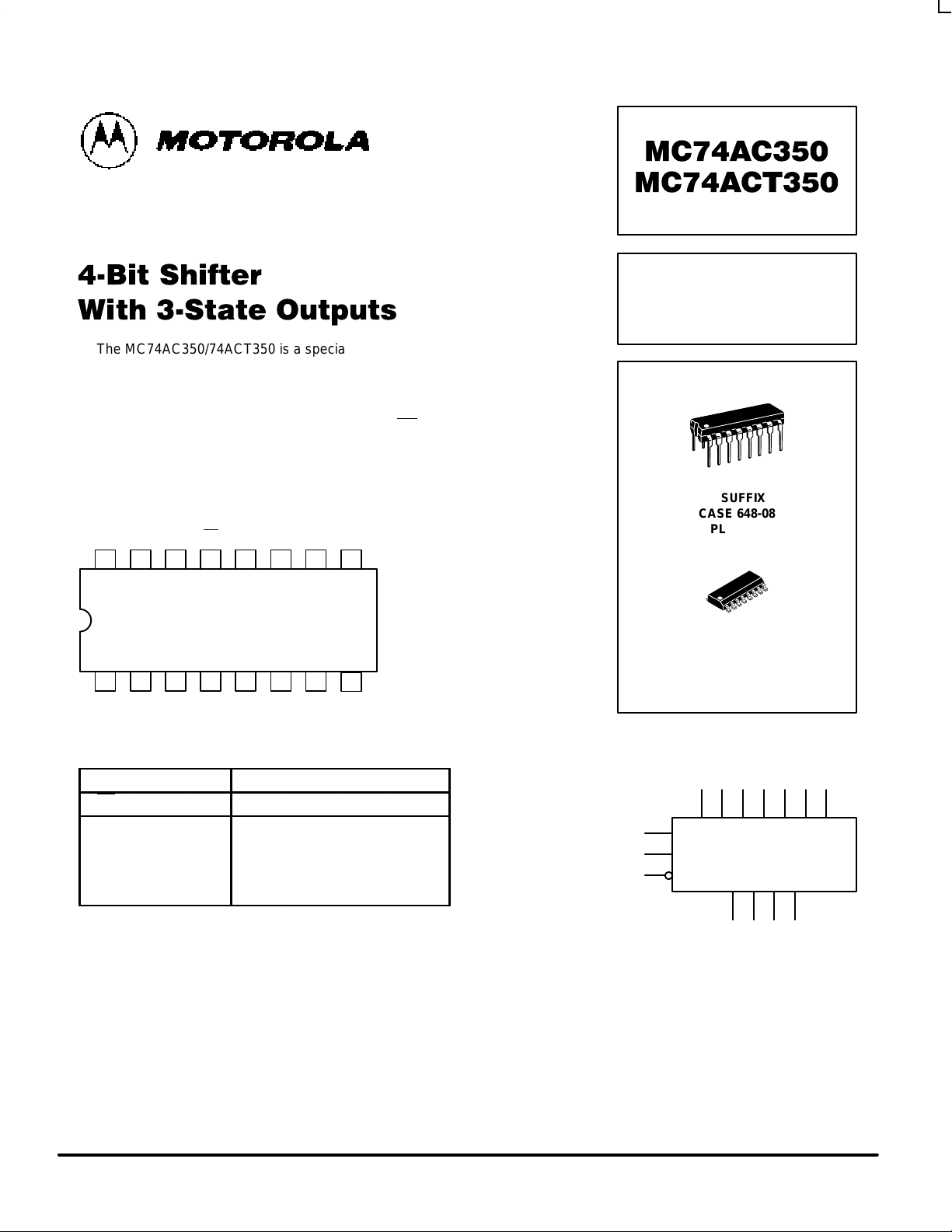
1516 14 13 12 11 10
21 3 4 5 6 7
V
CC
9
8
O0O1OE O2O3S0S
1
I
–3I–2I–1I0I1I2I3
GND
TRUTH TABLE
Inputs Outputs
OE S
1
S
0
O
0
O
1
O
2
O
3
H X X Z Z Z Z
L L L I
0
I
1
I
2
I
3
L L H I
–1
I
0
I
1
I
2
L H L I
–2
I
–1
I
0
I
1
L H H I
–3
I
–2
I
–1
I
0
H = HIGH Voltage Level
L = LOW Voltage Level
X = Immaterial
4-BIT SHIFTER
WITH 3-STATE
OUTPUTS
N SUFFIX
CASE 648-08
PLASTIC
D SUFFIX
CASE 751B-05
PLASTIC
LOGIC SYMBOL
OE
S
1
S
0
O0O1O2O
3
I–3I–2I–1I0I1I2I
3
13
9
10
15 14 12 11
1 2 3 4 5 6 7
Page 2
MC74AC350 MC74ACT350
5-2
FACT DATA
FUNCTIONAL DESCRIPTION
The MC74AC350/74ACT350 is operationally equivalent to
a 4-input multiplexer with the inputs connected so that the
select code causes successive one-bit shifts of the data word.
This internal connection makes it possible to perform shifts of
0, 1, 2 or 3 places on words of any length.
A 7-bit data word is introduced at the In inputs and is shifted
according to the code applied to the select inputs S0, S1.
Outputs O0–O3 are 3-state, controlled by an active-LOW
output enable (OE
). When OE is LOW, data outputs will follow
selected data inputs; when HIGH, the data outputs will be
forced to the high-impedance state. This feature allows
shifters to be cascaded on the same output lines or to a
common bus. The shift function can be logical, with zeros
pulled in at either or both ends of the shifting field; arithmetic,
where the sign bit is repeated during a shift down; or end
around, where the data word forms a continuous loop.
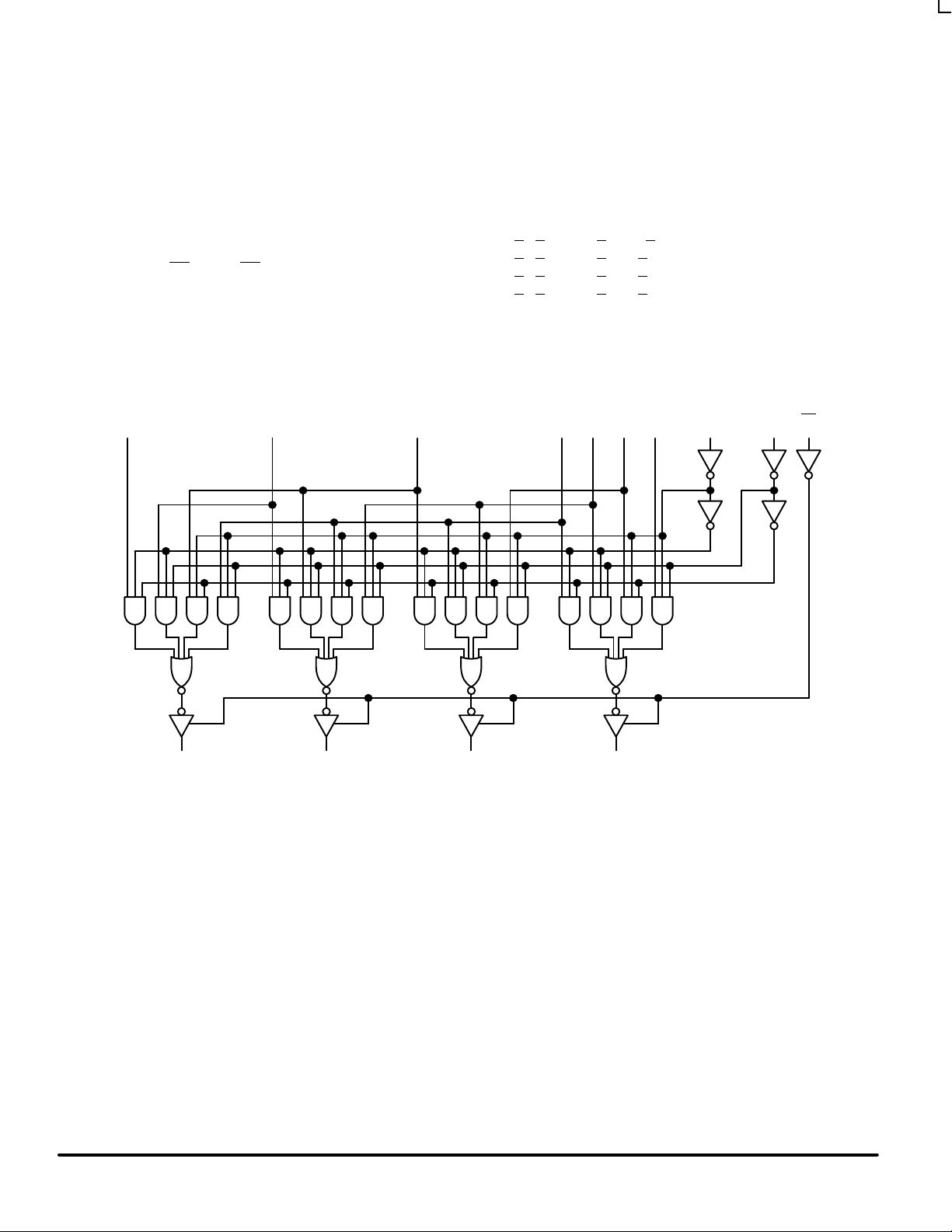
LOGIC EQUATIONS
O0=S
0 S1 I0+S0 S1 I–1+S0 S1 I–2+S0 S1 I–3
O1=S
0 S1 I1+S0 S1 I0+S0 S1 I–1+S0 S1 II–2
O2=S
0 S1 I2+S0 S1 I1+S0 S1 I0+S0 S1 I–1
O3=S
0 S1 I3+S0 S1 I2+S0 S1 I1+S0 S1 I0
LOGIC DIAGRAM
I
–3
I
–2
I
–1
I0I1I2I
3
S
1
S0OE
O
0
O
1
O
2
O
3
Page 3
MC74AC350 MC74ACT350
5-3
FACT DATA
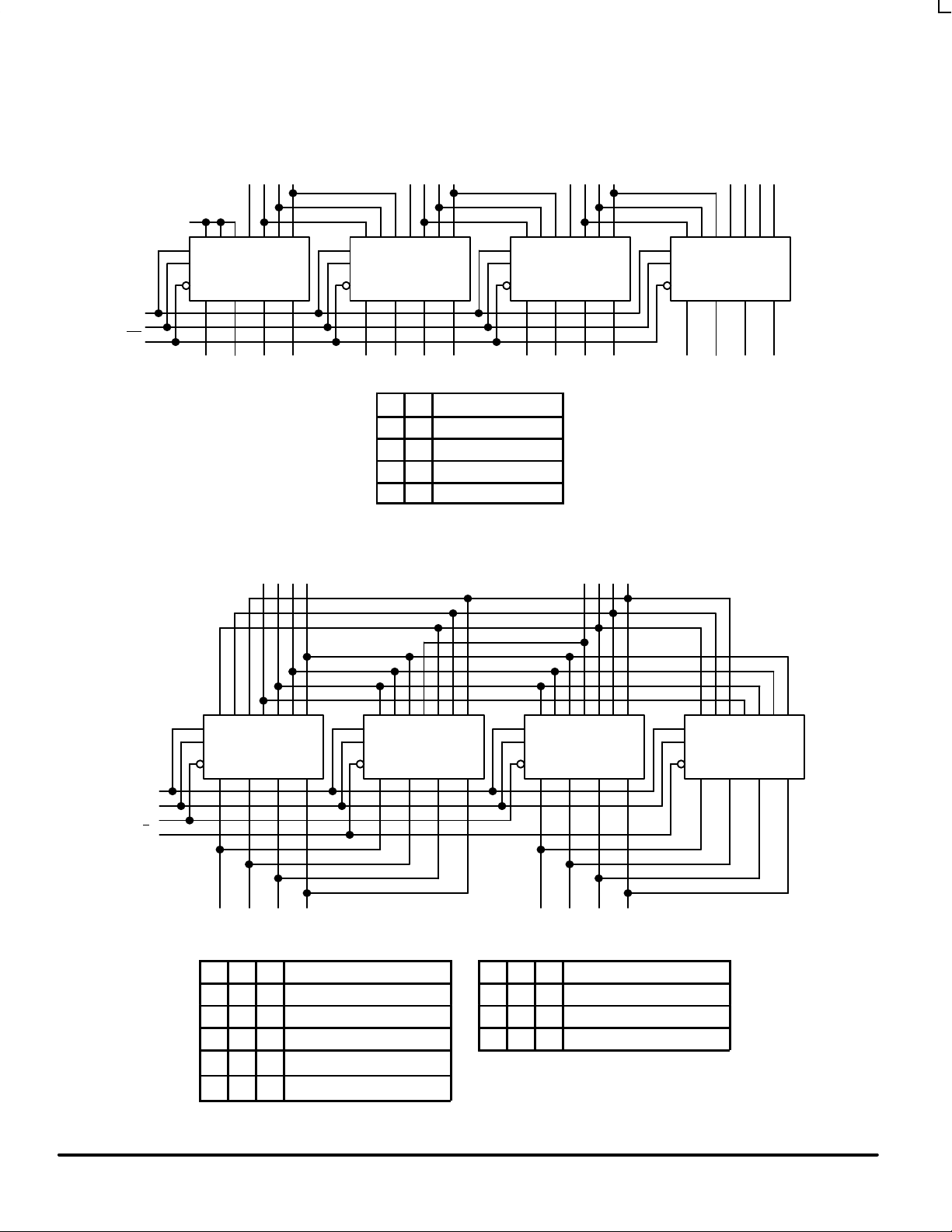
APPLICATIONS
16-Bit Shift-Up 0 to 3 Places, Zero Backfill
GND
S
0
S
1
OE
S
0
S
1
OE
Y0Y1Y2Y
3
I–3I–1I0I1I2I
3
I
–2
S
0
S
1
OE
Y0Y1Y2Y
3
I–3I–1I0I1I2I
3
I
–2
S
0
S
1
OE
Y0Y1Y2Y
3
I–3I–1I0I1I2I
3
I
–2
S
0
S
1
OE
Y0Y1Y2Y
0
I–3I–1I0I1I2I
3
I
–2
0 1 2 3 4 5 6 7 8 9 10 11 12 13 14 15
0 1 2 3 4 5 6 7 8 9 10 11 12 13 14 15
S1S
0
L L NO SHIFT
L H SHIFT 1 PLACE
H L SHIFT 2 PLACES
H H SHIFT 3 PLACES
S
0
S
1
S
2
S
0
S
1
OE
Y0Y1Y2Y
3
I–3I–1I0I1I2I
3
I
–2
S
0
S
1
OE
Y0Y1Y2Y
3
I–3I–1I0I1I2I
3
I
–2
S
0
S
1
OE
Y0Y1Y2Y
3
I–3I–1I0I1I2I
3
I
–2
S
0
S
1
OE
Y0Y1Y2Y
3
I–3I–1I0I1I2I
3
I
–2
0 1 2 3 4 5 6 7
0 1 2 3 4 5 6 7
S
2
8-Bit End Around Shift 0 to 7 Places
S2S1S
0
S2S1S
0
L L L NO SHIFT H L H SHIFT END AROUND 5
L L H SHIFT END AROUND 1 H H L SHIFT END AROUND 6
L H L SHIFT END AROUND 2 H H H SHIFT END AROUND 7
L H H SHIFT END AROUND 3
H L L SHIFT END AROUND 4
Page 4

MC74AC350 MC74ACT350
5-4
FACT DATA
13-Bit Twos Complement Scaler
S
0
S
1
OE
Y0Y1Y2Y
3
I–3I–1I0I1I2I
3
I
–2
S
0
S
1
OE
Y0Y1Y2Y
3
I–3I–1I0I1I2I
3
I
–2
S
0
S
1
OE
Y0Y1Y2Y
3
I–3I–1I0I1I2I
3
I
–2
12 11 10 9
12 11 10 9
8 7 6 5 4 3 2 1 S
8 7 6 5 4 3 2 1 S
S
0
S
1
S1S
0
SCALE
L L ÷ 8 1/8
L H ÷ 4 1/4
H L ÷ 2 1/2
H H NO CHANGE 1
MAXIMUM RATINGS*
Symbol Parameter Value Unit
V
CC
DC Supply Voltage (Referenced to GND) –0.5 to +7.0 V
V
in
DC Input Voltage (Referenced to GND) –0.5 to VCC +0.5 V
V
out
DC Output Voltage (Referenced to GND) –0.5 to VCC +0.5 V
I
in
DC Input Current, per Pin ±20 mA
I
out
DC Output Sink/Source Current, per Pin ±50 mA
I
CC
DC VCC or GND Current per Output Pin ±50 mA
T
stg
Storage Temperature –65 to +150 °C
* Maximum Ratings are those values beyond which damage to the device may occur. Functional operation should be restricted to the Recommended
Operating Conditions.
RECOMMENDED OPERATING CONDITIONS
Symbol Parameter Min Typ Max Unit
′AC 2.0 5.0 6.0
VCCSupply Voltage
′ACT 4.5 5.0 5.5
V
Vin, V
out
DC Input Voltage, Output Voltage (Ref. to GND) 0 V
CC
V
VCC @ 3.0 V 150
Input Rise and Fall Time (Note 1)
′AC Devices except Schmitt Inputs
VCC @ 4.5 V 40 ns/V
r
, t
f
′AC Devices except Schmitt Inputs
VCC @ 5.5 V 25
VCC @ 4.5 V 10
tr, t
f
Input Rise and Fall Time (Note 2)
′ACT Devices except Schmitt Inputs
VCC @ 5.5 V 8.0
ns/V
T
J
Junction Temperature (PDIP) 140 °C
T
A
Operating Ambient Temperature Range –40 25 85 °C
I
OH
Output Current — High –24 mA
I
OL
Output Current — Low 24 mA
1. Vin from 30% to 70% VCC; see individual Data Sheets for devices that differ from the typical input rise and fall times.
2. Vin from 0.8 V to 2.0 V; see individual Data Sheets for devices that differ from the typical input rise and fall times.
tr, t
f
Input Rise and Fall Time (Note 2)
Page 5

MC74AC350 MC74ACT350
5-5
FACT DATA
DC CHARACTERISTICS
74AC 74AC
Symbol
Parameter
V
CC
(V)
TA = +25°C
TA =
–40°C to +85°C
Unit
Conditions
Typ Guaranteed Limits
V
IH
3.0 1.5 2.1 2.1 V
OUT
= 0.1 V
4.5 2.25 3.15 3.15 V or VCC – 0.1 V
5.5 2.75 3.85 3.85
V
IL
3.0 1.5 0.9 0.9 V
OUT
= 0.1 V
4.5 2.25 1.35 1.35 V or VCC – 0.1 V
5.5 2.75 1.65 1.65
V
OH
3.0 2.99 2.9 2.9 I
OUT
= –50 µA
4.5 4.49 4.4 4.4 V
5.5 5.49 5.4 5.4
*VIN = VIL or V
IH
3.0 2.56 2.46
–12 mA
4.5 3.86 3.76
V
I
OH
–24 mA
5.5 4.86 4.76 –24 mA
V
OL
3.0 0.002 0.1 0.1 I
OUT
= 50 µA
4.5 0.001 0.1 0.1 V
5.5 0.001 0.1 0.1
*VIN = VIL or V
IH
3.0 0.36 0.44
12 mA
4.5 0.36 0.44
V
I
OL
24 mA
5.5 0.36 0.44 24 mA
I
IN
5.5
±0.1
±1.0
µA
VI = VCC, GND
I
OZ
VI (OE) = VIL, V
IH
5.5 ±0.5 ±5.0 µA VI = VCC, GND
VO = VCC, GND
I
OLD
5.5 75 mA V
OLD
= 1.65 V Max
I
OHD
Output Current
5.5 –75 mA V
OHD
= 3.85 V Min
I
CC
5.5
8.080µA
VIN = VCC or GND
* All outputs loaded; thresholds on input associated with output under test.
†Maximum test duration 2.0 ms, one output loaded at a time.
Note: IIN and ICC @ 3.0 V are guaranteed to be less than or equal to the respective limit @ 5.5 V VCC.
Minimum High Level
Input Voltage
Maximum Low Level
Input Voltage
Minimum High Level
Output Voltage
Maximum Low Level
Output Voltage
Maximum Input
Leakage Current
Maximum
3-State
Current
†Minimum Dynamic
Maximum Quiescent
Supply Current
Page 6

MC74AC350 MC74ACT350
5-6
FACT DATA
AC CHARACTERISTICS (For Figures and Waveforms — See Section 3)
74AC 74AC
Symbol
Parameter
VCC*
(V)
TA = +25°C
CL = 50 pF
TA = –40°C
to +85°C
CL = 50 pF
Unit
Fig.
No.
Min Typ Max Min Max
Propagation Delay
3.3 4.0 12.5 3.0 13.5
t
PLH
In to O
n
5.0 3.0 8.5 2.5 9.5
ns
3-5
Propagation Delay
3.3 4.0 12.5 3.0 13.5
t
PHL
In to O
n
5.0 3.0 8.5 2.5 9.5
ns
3-5
Propagation Delay
3.3 5.0 15.5 4.0 17.5
t
PLH
Sn to O
n
5.0 3.5 11.0 2.5 12.0
ns
3-6
Propagation Delay
3.3 5.0 15.5 4.5 17.5
t
PHL
Sn to O
n
5.0 3.5 11.0 3.0 12.0
ns
3-6
3.3 3.5 8.5 3.0 9.0
t
PZH
Output Enable to O
n
5.0 2.5 6.0 2.0 6.5
ns
3-7
3.3 3.5 11.0 2.5 12.0
t
PZL
Output Enable to O
n
5.0 2.5 7.5 2.0 8.0
ns
3-8
3.3 5.0 9.5 4.5 10.0
t
PHZ
Output Enable to O
n
5.0 4.5 8.0 4.0 8.5
ns
3-7
3.3 3.0 6.5 2.5 7.0
t
PLZ
Output Enable to O
n
5.0 2.5 6.0 2.0 6.5
ns
3-8
* Voltage Range 3.3 V is 3.3 V ±0.3 V.
Voltage Range 5.0 V is 5.0 V ±0.5 V.
Page 7

MC74AC350 MC74ACT350
5-7
FACT DATA
DC CHARACTERISTICS
74ACT 74ACT
Symbol
Parameter
V
CC
(V)
TA = +25°C
TA =
–40°C to +85°C
Unit
Conditions
Typ Guaranteed Limits
V
IH
4.5 1.5 2.0 2.0
V
OUT
= 0.1 V
5.5 1.5 2.0 2.0
V
or VCC – 0.1 V
V
IL
4.5 1.5 0.8 0.8
V
OUT
= 0.1 V
5.5 1.5 0.8 0.8
V
or VCC – 0.1 V
V
OH
4.5 4.49 4.4 4.4
I
OUT
= –50 µA
5.5 5.49 5.4 5.4
V
*VIN = VIL or V
IH
4.5 3.86 3.76 V
–24 mA
5.5 4.86 4.76
I
OH
–24 mA
V
OL
4.5 0.001 0.1 0.1
I
OUT
= 50 µA
5.5 0.001 0.1 0.1
V
*VIN = VIL or V
IH
4.5 0.36 0.44 V
24 mA
5.5 0.36 0.44
I
OL
24 mA
I
IN
5.5
±0.1
±1.0
µA
VI = VCC, GND
∆I
CCT
Additional Max. ICC/Input 5.5 0.6 1.5 mA VI = VCC – 2.1 V
I
OZ
VI (OE) = VIL, V
IH
5.5 ±0.5 ±5.0 µA VI = VCC, GND
VO = VCC, GND
I
OLD
5.5 75 mA V
OLD
= 1.65 V Max
I
OHD
Output Current
5.5 –75 mA V
OHD
= 3.85 V Min
I
CC
5.5
8.080µA
VIN = VCC or GND
* All outputs loaded; thresholds on input associated with output under test.
†Maximum test duration 2.0 ms, one output loaded at a time.
Minimum High Level
Input Voltage
Maximum Low Level
Input Voltage
Minimum High Level
Output Voltage
Maximum Low Level
Output Voltage
Maximum Input
Leakage Current
Maximum
3-State
Current
†Minimum Dynamic
Maximum Quiescent
Supply Current
Page 8

MC74AC350 MC74ACT350
5-8
FACT DATA
AC CHARACTERISTICS (For Figures and Waveforms — See Section 3)
74ACT 74ACT
Symbol
Parameter
VCC*
(V)
TA = +25°C
CL = 50 pF
TA = –40°C
to +85°C
CL = 50 pF
Unit
Fig.
No.
Min Typ Max Min Max
t
PLH
5.0
4.0
11.5
3.0
13.5ns3-6
t
PHL
5.0
4.0
11.5
3.0
13.5ns3-6
t
PLH
5.0
4.5
13.0
3.5
15.5ns3-6
t
PHL
5.0
4.5
13.0
3.5
15.5ns3-6
t
PZH
Output Enable to O
n
5.0 4.0 9.0 3.0 10.0 ns 3-7
t
PZL
Output Enable to O
n
5.0 4.0 10.0 3.0 11.5 ns 3-8
t
PHZ
Output Enable to O
n
5.0 4.0 10.0 3.0 11.0 ns 3-7
t
PLZ
Output Enable to O
n
5.0 4.0 8.0 3.0 9.0 ns 3-8
* Voltage Range 5.0 V is 5.0 V ±0.5 V.
CAPACITANCE
Symbol Parameter
Value
Typ
Unit Test Conditions
C
IN
Input Capacitance 4.5 pF VCC = 5.0 V
C
PD
Power Dissipation Capacitance 40.0 pF VCC = 5.0 V
Propagation Delay
In to O
n
Propagation Delay
In to O
n
Propagation Delay
Sn to O
n
Propagation Delay
Sn to O
n
Page 9

MC74AC350 MC74ACT350
5-9
FACT DATA
OUTLINE DIMENSIONS
N SUFFIX
PLASTIC DIP PACKAGE
CASE 648–08
ISSUE R
D SUFFIX
PLASTIC SOIC PACKAGE
CASE 751B–05
ISSUE J
NOTES:
1. DIMENSIONING AND TOLERANCING PER
ANSI Y14.5M, 1982.
2. CONTROLLING DIMENSION: MILLIMETER.
3. DIMENSIONS A AND B DO NOT INCLUDE
MOLD PROTRUSION.
4. MAXIMUM MOLD PROTRUSION 0.15 (0.006)
PER SIDE.
5. DIMENSION D DOES NOT INCLUDE DAMBAR
PROTRUSION. ALLOWABLE DAMBAR
PROTRUSION SHALL BE 0.127 (0.005) TOTAL
IN EXCESS OF THE D DIMENSION AT
MAXIMUM MATERIAL CONDITION.
1 8
16 9
SEATING
PLANE
F
J
M
R
X 45
_
G
8 PLP
–B–
–A–
M
0.25 (0.010) B
S
–T–
D
K
C
16 PL
S
B
M
0.25 (0.010) A
S
T
DIM MIN MAX MIN MAX
INCHESMILLIMETERS
A 9.80 10.00 0.386 0.393
B 3.80 4.00 0.150 0.157
C 1.35 1.75 0.054 0.068
D 0.35 0.49 0.014 0.019
F 0.40 1.25 0.016 0.049
G 1.27 BSC 0.050 BSC
J 0.19 0.25 0.008 0.009
K 0.10 0.25 0.004 0.009
M 0 7 0 7
P 5.80 6.20 0.229 0.244
R 0.25 0.50 0.010 0.019
_ _ _ _
NOTES:
1. DIMENSIONING AND TOLERANCING PER ANSI
Y14.5M, 1982.
2. CONTROLLING DIMENSION: INCH.
3. DIMENSION L TO CENTER OF LEADS WHEN
FORMED PARALLEL.
4. DIMENSION B DOES NOT INCLUDE MOLD FLASH.
5. ROUNDED CORNERS OPTIONAL.
–A–
B
F
C
S
H
G
D
J
L
M
16 PL
SEATING
1 8
916
K
PLANE
–T–
M
A
M
0.25 (0.010) T
DIM MIN MAX MIN MAX
MILLIMETERSINCHES
A 0.740 0.770 18.80 19.55
B 0.250 0.270 6.35 6.85
C 0.145 0.175 3.69 4.44
D 0.015 0.021 0.39 0.53
F 0.040 0.70 1.02 1.77
G 0.100 BSC 2.54 BSC
H 0.050 BSC 1.27 BSC
J 0.008 0.015 0.21 0.38
K 0.110 0.130 2.80 3.30
L 0.295 0.305 7.50 7.74
M 0 10 0 10
S 0.020 0.040 0.51 1.01
____
How to reach us:
USA/EUROPE: Motorola Literature Distribution; JAPAN: Nippon Motorola Ltd.; Tatsumi–SPD–JLDC, Toshikatsu Otsuki,
P.O. Box 20912; Phoenix, Arizona 85036. 1–800–441–2447 6F Seibu–Butsuryu–Center, 3–14–2 Tatsumi Koto–Ku, Tokyo 135, Japan. 03–3521–8315
MFAX: RMFAX0@email.sps.mot.com –TOUCHTONE (602) 244–6609 HONG KONG: Motorola Semiconductors H.K. Ltd.; 8B Tai Ping Industrial Park,
INTERNET: http://Design–NET.com 51 Ting Kok Road, Tai Po, N.T., Hong Kong. 852–26629298
Motorola reserves the right to make changes without further notice to any products herein. Motorola makes no warranty , representation or guarantee regarding
the suitability of its products for any particular purpose, nor does Motorola assume any liability arising out of the application or use of any product or circuit, and
specifically disclaims any and all liability , including without limitation consequential or incidental damages. “Typical” parameters can and do vary in different
applications. All operating parameters, including “T ypicals” must be validated for each customer application by customer’s technical experts. Motorola does
not convey any license under its patent rights nor the rights of others. Motorola products are not designed, intended, or authorized for use as components in
systems intended for surgical implant into the body, or other applications intended to support or sustain life, or for any other application in which the failure of
the Motorola product could create a situation where personal injury or death may occur. Should Buyer purchase or use Motorola products for any such
unintended or unauthorized application, Buyer shall indemnify and hold Motorola and its officers, employees, subsidiaries, affiliates, and distributors harmless
against all claims, costs, damages, and expenses, and reasonable attorney fees arising out of, directly or indirectly, any claim of personal injury or death
associated with such unintended or unauthorized use, even if such claim alleges that Motorola was negligent regarding the design or manufacture of the part.
Motorola and are registered trademarks of Motorola, Inc. Motorola, Inc. is an Equal Opportunity/Affirmative Action Employer.
MC74AC350/D
*MC74AC350/D*
◊
 Loading...