

Datasheet MC74ACT299DW, MC74ACT299DWR2, MC74ACT299N, MC74AC299N, MC74AC299DWR2 Datasheet (MOTOROLA)
Page 1
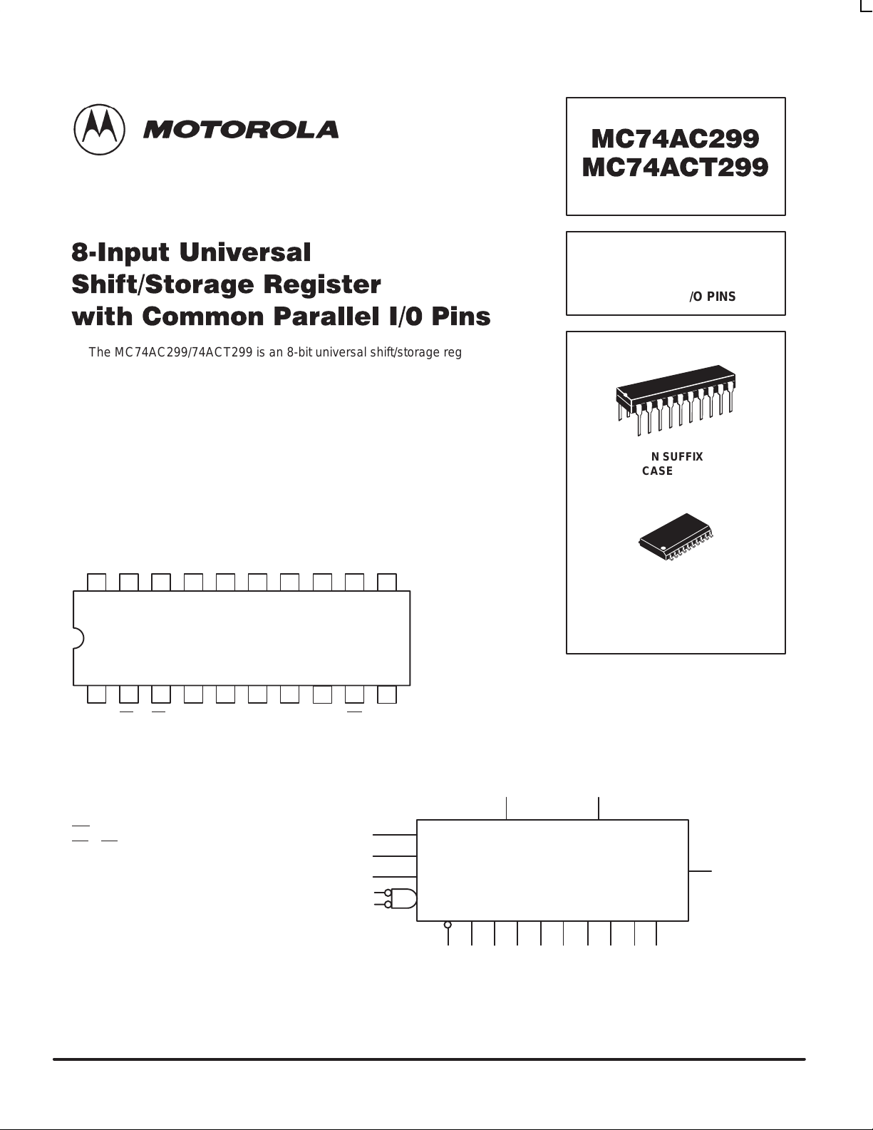
MC74AC299
MC74ACT299
8ĆInput Universal
Shift/Storage Register
with Common Parallel I/0 Pins
The MC74AC299/74ACT299 is an 8-bit universal shift/storage register
with 3-state outputs. Four modes of operation are possible: hold (store), shift left,
shift right and load data. The parallel load inputs and flip-flop outputs are multiplexed
to reduce the total number of package pins. Additional outputs are provided for
flip-flops Q0, Q7 to allow easy serial cascading. A separate active LOW Master
Reset is used to reset the register.
• Common Parallel I/O for Reduced Pin Count
• Additional Serial Inputs and Outputs for Expansion
• Four Operating Modes: Shift Left, Shift Right, Load and Store
• 3-State Outputs for Bus-Oriented Applications
• Outputs Source/Sink 24 mA
•′ACT299 Has TTL Compatible Inputs
S1DS7Q7I/O7I/O5I/O3I/O1CP DS
V
CC
1920 18 17 16 15 14
13
0
12
11
8-INPUT UNIVERSAL
SHIFT/STORAGE REGISTER
WITH COMMON
PARALLEL I/O PINS
N SUFFIX
CASE 738-03
PLASTIC
DW SUFFIX
CASE 751D-04
PLASTIC
21 34567
S0OE
1OE2
PIN NAMES
CP Clock Pulse Input
DS
0
DS
7
S0, S
MR Asynchronous Master Reset
OE
OE23-State Output Enable Inputs
1,
I/O0–I/O7Parallel Data Inputs or
Q0, Q
Serial Data Input for Right Shift
Serial Data Input for Left Shift
Mode Select Inputs
1
3-State Parallel Outputs
Serial Outputs
7
I/O6I/O4I/O2I/O0Q0MR GND
9
8
10
LOGIC SYMBOL
S
0
S
1
CP
OE
MR Q0I/O
DS
0
I/O
I/O
DS
7
Q
7
I/O
I/O
I/O
4
3
I/O
6
5
7
0
I/O
2
1
FACT DAT A
5-1
Page 2
MC74AC299 MC74ACT299
LOGIC DIAGRAM
DS
7
Q
7
DQ
C
D
CP
DQ
C
D
CP
DQ
C
D
CP
DQ
C
D
CP
DQ
C
D
I/O
7
I/O
6
I/O
5
I/O
4
I/O
3
CP
DQ
C
D
CP
DQ
C
D
CP
DQ
C
D
S
0
S
1
DS
0
CP
Q0MR
OE
1
Please note that this diagram is provided only for the understanding of logic
operations and should not be used to estimate propagation delays.
I/O
2
I/O
1
I/O
0
OE
2
FACT DAT A
5-2
Page 3
FUNCTIONAL DESCRIPTION
Response
VCCSupply Voltage
V
AC Devices exce t Schmitt In uts
t
t
()
ns/V
MC74AC299 MC74ACT299
The MC74AC299/74ACT299 contains eight edge-triggered
D-type flip-flops and the interstage logic necessary to perform
synchronous shift left, shift right, parallel load and hold
operations. The type of operation is determined by S0 and S1,
as shown in the Truth T able. All flip-flop outputs are brought out
through 3-state buffers to separate I/O pins that also serve as
data inputs in the parallel load mode. Q0 and Q7 are also
brought out on other pins for expansion in serial shifting of
longer words.
A LOW signal on MR
overrides the Select and CP inputs
and resets the flip-flops. All other state changes are initiated
by the rising edge of the clock. Inputs can change when the
clock is in either state provided only that the recommended
setup and hold times, relative to the rising edge of CP, are
TRUTH TABLE
Inputs
MR S1S0CP
L X X X Asynchronous Reset; Q0–Q7 = LOW
H H H Parallel Load; I/On Q
H L H Shift Rights; DS0 Q0, Q0 Q1, etc.
H H L Shift Left; DS7 Q7, Q7 Q6, etc.
H L L X Hold
H = HIGH Voltage Level
L = LOW Voltage Level
X = Immaterial
= LOW-to-HIGH Transition
n
observed.
A HIGH signal on either OE
or OE2 disables the 3-state
1
buffers and puts the I/O pins in the high impedance state. In
this condition the shift, hold, load and reset operations can still
occur. The 3-state buffers are also disabled by HIGH signals
on both S0 and S1 in preparation for a parallel load operation.
MAXIMUM RATINGS*
Symbol Parameter Value Unit
V
CC
V
in
V
out
I
in
I
out
I
CC
T
stg
* Maximum Ratings are those values beyond which damage to the device may occur. Functional operation should be restricted to the Recommended
Operating Conditions.
DC Supply Voltage (Referenced to GND) –0.5 to +7.0 V
DC Input Voltage (Referenced to GND) –0.5 to VCC +0.5 V
DC Output Voltage (Referenced to GND) –0.5 to VCC +0.5 V
DC Input Current, per Pin ±20 mA
DC Output Sink/Source Current, per Pin ±50 mA
DC VCC or GND Current per Output Pin ±50 mA
Storage Temperature –65 to +150 °C
RECOMMENDED OPERATING CONDITIONS
Symbol Parameter Min Typ Max Unit
Vin, V
out
tr, t
f
,
r
f
T
J
T
A
I
OH
I
OL
1. Vin from 30% to 70% VCC; see individual Data Sheets for devices that differ from the typical input rise and fall times.
2. Vin from 0.8 V to 2.0 V; see individual Data Sheets for devices that differ from the typical input rise and fall times.
DC Input Voltage, Output Voltage (Ref. to GND) 0 V
Input Rise and Fall Time (Note 1)
′AC Devices except Schmitt Inputs
Input Rise and Fall Time (Note 2)
′ACT Devices except Schmitt Inputs
Junction Temperature (PDIP) 140 °C
Operating Ambient Temperature Range –40 25 85 °C
Output Current — High –24 mA
Output Current — Low 24 mA
pp
VCC @ 3.0 V 150
VCC @ 4.5 V 40 ns/V
VCC @ 5.5 V 25
VCC @ 4.5 V 10
VCC @ 5.5 V 8.0
FACT DAT A
5-3
′AC 2.0 5.0 6.0
′ACT 4.5 5.0 5.5
CC
V
Page 4

MC74AC299 MC74ACT299
V
V
5.5
±0.1
±1.0
µA
V
I
V
CC
GND
Current
5.5
±0.6
±6.0
µA
V
I
V
CC
GND
5.5
8.080µA
V
IN
V
CC
GND
DC CHARACTERISTICS
74AC 74AC
V
Symbol Parameter
V
IH
V
IL
V
OH
V
OL
I
IN
I
OZT
I
OLD
I
OHD
I
CC
* All outputs loaded; thresholds on input associated with output under test.
†Maximum test duration 2.0 ms, one output loaded at a time.
Note: IIN and ICC @ 3.0 V are guaranteed to be less than or equal to the respective limit @ 5.5 V VCC.
Minimum High Level
Input Voltage
Maximum Low Level
Input Voltage
Minimum High Level
Output Voltage
Maximum Low Level
Output Voltage
Maximum Input
Leakage Current
Maximum 3-State
†Minimum Dynamic
Output Current
Maximum Quiescent
Supply Current
CC
(V)
3.0 1.5 2.1 2.1 V
4.5 2.25 3.15 3.15 V or VCC – 0.1 V
5.5 2.75 3.85 3.85
3.0 1.5 0.9 0.9 V
4.5 2.25 1.35 1.35 V or VCC – 0.1 V
5.5 2.75 1.65 1.65
3.0 2.99 2.9 2.9 I
4.5 4.49 4.4 4.4 V
5.5 5.49 5.4 5.4
3.0 2.56 2.46
4.5 3.86 3.76
5.5 4.86 4.76 –24 mA
3.0 0.002 0.1 0.1 I
4.5 0.001 0.1 0.1 V
5.5 0.001 0.1 0.1
3.0 0.36 0.44
4.5 0.36 0.44
5.5 0.36 0.44 24 mA
5.5 75 mA V
5.5 –75 mA V
TA = +25°C
Typ Guaranteed Limits
–40°C to +85°C
TA =
Unit Conditions
= 0.1 V
OUT
= 0.1 V
OUT
= –50 µA
OUT
*VIN = VIL or V
–12 mA
I
OH
OUT
*VIN = VIL or V
I
OL
VI (OE) = VIL, V
VO = VCC, GND
= 50 µA
=
=
= 1.65 V Max
OLD
= 3.85 V Min
OHD
=
–24 mA
12 mA
24 mA
,
,
or
IH
IH
IH
FACT DAT A
5-4
Page 5

MC74AC299 MC74ACT299
f
MHz
3-3
t
PLH
ns
3-6
t
PHL
ns
3-6
t
PLH
ns
3-6
t
PHL
ns
3-6
t
PHL
ns
3-6
t
PHL
ns
3-6
t
PZH
ns
3-7
t
PZL
ns
3-8
t
PHZ
ns
3-7
t
PLZ
ns
3-8
AC CHARACTERISTICS (For Figures and Waveforms — See Section 3)
Symbol Parameter
max
* Voltage Range 3.3 V is 3.3 V ±0.3 V.
Voltage Range 5.0 V is 5.0 V ±0.5 V.
Maximum Input
Frequency 5.0 130 105
Propagation Delay
CP to Q0 or Q
Propagation Delay
CP to Q0 or Q
Propagation Delay
CP to I/O
Propagation Delay
CP to I/O
Propagation Delay
MR to Q0 or Q
Propagation Delay
MR to I/O
Output Enable Time
OE to I/O
Output Enable Time
OE to I/O
Output Disable Time
OE to I/O
Output Disable Time
OE to I/O
7
7
n
n
7
n
n
n
n
n
VCC*
(V)
Min Typ Max Min Max
3.3 90 80
3.3 8.5 20.5 7.0 22
5.0 5.5 14 4.5 15
3.3 8.5 21.5 7.0 23
5.0 5.5 14.5 5.0 16
3.3 9.0 20.5 7.5 22.5
5.0 6.0 14.5 5.0 16
3.3 10 23 8.5 24.5
5.0 6.5 16 6.0 17.5
3.3 9.0 22.5 7.5 25.0
5.0 5.5 15.5 5.0 17.0
3.3 9.0 21.5 7.5 24.0
5.0 5.5 15.0 5.0 16.5
3.3 7.0 18 6.0 19.5
5.0 4.5 12.5 4.0 13.5
3.3 7.0 18 6.0 20.5
5.0 5.0 12.5 4.0 14
3.3 6.5 18.5 5.5 19.5
5.0 3.5 14 3.0 15
3.3 5.5 17 4.5 19
5.0 3.5 12.5 2.0 13.5
74AC 74AC
TA = +25°C
CL = 50 pF
TA = –40°C
CL = 50 pF
to +85°C
Unit
Fig.
No.
-
-
-
-
-
-
-
-
-
-
-
FACT DAT A
5-5
Page 6

AC OPERATING REQUIREMENTS
t
ns
3-9
t
h
ns
3-9
t
ns
3-9
t
h
ns
3-9
t
ns
3-6
t
h
ns
3-6
twCP Pulse Width, LOW
ns
3-6
t
MR Pulse Width, LOW
ns
3-9
t
ns
3-9
Symbol Parameter
s
s
s
w
rec
* Voltage Range 3.3 V is 3.3 V ±0.3 V.
Voltage Range 5.0 V is 5.0 V ±0.5 V.
Setup Time, HIGH or LOW 3.3 8.0 8.5
S0 or S1 to CP 5.0 5.0 5.5
Hold Time, HIGH or LOW 3.3 0.5 0.5
S0 or S1 to CP 5.0 1.0 1.0
Setup Time, HIGH or LOW 3.3 5.5 6.0
I/On to CP 5.0 3.5 4.0
Hold Time, HIGH or LOW 3.3 0 0
I/On to CP 5.0 1.0 1.0
Setup Time, HIGH or LOW 3.3 6.5 7.0
DS0 or DS7 to CP 5.0 4.0 4.5
Hold Time, HIGH or LOW 3.3 0 0.5
DS0 or DS7 to CP 5.0 1.0 1.0
Recovery TIme 3.3 1.5 1.5
MR to CP 5.0 1.5 1.5
MC74AC299 MC74ACT299
74AC 74AC
VCC*
(V)
3.3 4.5 5.0
5.0 3.5 3.5
3.3 4.5 5.0
5.0 3.5 3.5
TA = +25°C
CL = 50 pF
Typ Guaranteed Minimum
TA = –40°C
to +85°C
CL = 50 pF
Unit
Fig.
No.
-
-
-
-
-
-
-
-
-
FACT DAT A
5-6
Page 7

MC74AC299 MC74ACT299
V
V
V
I
OH
V
I
OL
5.5
±0.1
±1.0
µA
V
I
V
CC
GND
Current
5.5
±0.6
±6.0
µA
V
I
V
CC
GND
5.5
8.080µA
V
IN
V
CC
GND
DC CHARACTERISTICS
Symbol Parameter
V
IH
V
IL
V
OH
V
OL
I
IN
I
OZT
∆I
CCT
I
OLD
I
OHD
I
CC
* All outputs loaded; thresholds on input associated with output under test.
†Maximum test duration 2.0 ms, one output loaded at a time.
Minimum High Level
Input Voltage
Maximum Low Level
Input Voltage
Minimum High Level
Output Voltage
Maximum Low Level
Output Voltage
Maximum Input
Leakage Current
Maximum 3-State
Additional Max. ICC/Input 5.5 0.6 1.5 mA VI = VCC – 2.1 V
†Minimum Dynamic
Output Current
Maximum Quiescent
Supply Current
V
74ACT 74ACT
CC
(V)
4.5 1.5 2.0 2.0
5.5 1.5 2.0 2.0
4.5 1.5 0.8 0.8
5.5 1.5 0.8 0.8
4.5 4.49 4.4 4.4
5.5 5.49 5.4 5.4
4.5 3.86 3.76 V
5.5 4.86 4.76
4.5 0.001 0.1 0.1
5.5 0.001 0.1 0.1
4.5 0.36 0.44 V
5.5 0.36 0.44
5.5 75 mA V
5.5 –75 mA V
TA = +25°C
Typ Guaranteed Limits
TA =
–40°C to +85°C
Unit Conditions
V
= 0.1 V
OUT
or VCC – 0.1 V
V
= 0.1 V
OUT
or VCC – 0.1 V
I
= –50 µA
OUT
*VIN = VIL or V
–24 mA
–24 mA
I
= 50 µA
OUT
*VIN = VIL or V
24 mA
24 mA
=
,
VI (OE) = VIL, V
=
= 1.65 V Max
OLD
= 3.85 V Min
OHD
=
,
or
VO = VCC, GND
IH
IH
IH
FACT DAT A
5-7
Page 8

MC74AC299 MC74ACT299
f
5.0
120
110
MHz
3-3
t
PLH
5.0
4.0
12.5
3.014ns
3-6
t
PHL
5.0
4.0
13.5
3.515ns
3-6
t
PLH
5.0
4.5
12.5
4.5
13.5ns3-6
t
PHL
5.0
5.0154.5
16.5ns3-6
t
PHL
5.0
4.0154.018ns
3-6
t
PHL
5.0
4.0
14.5
3.5
17.5ns3-6
t
PZH
5.0
2.5121.513ns
3-7
t
PZL
5.0
2.0121.5
13.5ns3-8
t
PHZ
5.0
2.0
12.5
2.0
13.5ns3-7
t
PLZ
5.0
2.5
11.5
2.0
12.5ns3-8
AC CHARACTERISTICS (For Figures and Waveforms — See Section 3)
Symbol Parameter
max
* Voltage Range 5.0 V is 5.0 V ±0.5 V.
Maximum Input
Frequency
Propagation Delay
CP to Q0 or Q
Propagation Delay
CP to Q0 or Q
Propagation Delay
CP to I/O
Propagation Delay
CP to I/O
Propagation Delay
MR to Q0 or Q
Propagation Delay
MR to I/O
Output Enable Time
OE to I/O
Output Enable Time
OE to I/O
Output Disable Time
OE to I/O
Output Disable Time
OE to I/O
7
7
n
n
7
n
n
n
n
n
VCC*
(V)
Min Typ Max Min Max
74ACT 74ACT
TA = +25°C
CL = 50 pF
TA = –40°C
to +85°C
CL = 50 pF
Unit
Fig.
No.
-
-
-
-
-
-
-
-
-
-
-
FACT DAT A
5-8
Page 9

AC OPERATING REQUIREMENTS
t
5.0
5.0
5.5
ns
3-9
t
h
5.0
1.0
1.0
ns
3-9
t
5.0
4.0
4.5
ns
3-9
t
h
5.0
1.0
1.0
ns
3-9
t
5.0
4.5
5.0
ns
3-6
t
h
5.0
1.0
1.0
ns
3-6
t
5.0
4.0
4.5
ns
3-9
t
MR Pulse Width, LOW
5.0
3.5
3.5
ns
3-9
t
5.0
1.5
1.5
ns
3-9
Symbol Parameter
s
s
s
w
Setup Time, HIGH or LOW
S0 or S1 to CP
Hold Time, HIGH or LOW
S0 or S1 to CP
Setup Time, HIGH or LOW
I/On to CP
Hold Time, HIGH or LOW
I/On to CP
Setup Time, HIGH or LOW
DS0 or DS7 to CP
Hold Time, HIGH or LOW
DS0 or DS7 to CP
CP Pulse Width
HIGH or LOW
MC74AC299 MC74ACT299
74ACT 74ACT
VCC*
(V)
TA = +25°C
CL = 50 pF
Typ Guaranteed Minimum
TA = –40°C
to +85°C
CL = 50 pF
Unit
Fig.
No.
-
-
-
-
-
-
-
w
rec
* Voltage Range 5.0 V is 5.0 V ±0.5 V.
Recovery Time
MR to CP
CAPACITANCE
Symbol Parameter
C
IN
C
PD
Input Capacitance 4.5 pF VCC = 5.0 V
Power Dissipation Capacitance 170 pF VCC = 5.0 V
Value
Typ
-
-
Unit Test Conditions
FACT DAT A
5-9
Page 10

–T–
SEATING
PLANE
20
MC74AC299 MC74ACT299
OUTLINE DIMENSIONS
N SUFFIX
–A–
20
1
11
10
E
FG
20 PL
D
0.25 (0.010) T
–A–
11
–B–
1
20X
D
0.010 (0.25) B
10
M
S
A
T
S
C
18X
G
K
PLASTIC DIP PACKAGE
CASE 738–03
ISSUE E
B
C
K
N
M
M
A
DW SUFFIX
PLASTIC SOIC PACKAGE
CASE 751D–04
ISSUE E
P10X
M
B
J
F
–T–
0.010 (0.25)
SEATING
PLANE
M
M
L
J
20 PL
0.25 (0.010) T
R
X 45
NOTES:
1. DIMENSIONING AND TOLERANCING PER
ANSI Y14.5M, 1982.
2. CONTROLLING DIMENSION: INCH.
3. DIMENSION L TO CENTER OF LEAD WHEN
FORMED PARALLEL.
4. DIMENSION B DOES NOT INCLUDE MOLD
FLASH.
DIM MIN MAX MIN MAX
A 25.66 27.171.010 1.070
B 6.10 6.600.240 0.260
C 3.81 4.570.150 0.180
D 0.39 0.550.015 0.022
M
M
B
_
E
F
G 2.54 BSC0.100 BSC
J 0.21 0.380.008 0.015
K 2.80 3.550.110 0.140
L 7.62 BSC0.300 BSC
M
M 0 15 0 15
N 0.51 1.010.020 0.040
NOTES:
1. DIMENSIONING AND TOLERANCING PER
ANSI Y14.5M, 1982.
2. CONTROLLING DIMENSION: MILLIMETER.
3. DIMENSIONS A AND B DO NOT INCLUDE
MOLD PROTRUSION.
4. MAXIMUM MOLD PROTRUSION 0.150
(0.006) PER SIDE.
5. DIMENSION D DOES NOT INCLUDE
DAMBAR PROTRUSION. ALLOWABLE
DAMBAR PROTRUSION SHALL BE 0.13
(0.005) TOTAL IN EXCESS OF D
DIMENSION AT MAXIMUM MATERIAL
CONDITION.
DIM MIN MAX MIN MAX
A 12.65 12.95 0.499 0.510
B 7.40 7.60 0.292 0.299
C 2.35 2.65 0.093 0.104
D 0.35 0.49 0.014 0.019
F 0.50 0.90 0.020 0.035
G 1.27 BSC 0.050 BSC
J 0.25 0.32 0.010 0.012
K 0.10 0.25 0.004 0.009
M 0 7 0 7
__
P 10.05 10.55 0.395 0.415
R 0.25 0.75 0.010 0.029
MILLIMETERSINCHES
1.27 BSC0.050 BSC
1.27 1.770.050 0.070
____
INCHESMILLIMETERS
__
Motorola reserves the right to make changes without further notice to any products herein. Motorola makes no warranty , representation or guarantee regarding
the suitability of its products for any particular purpose, nor does Motorola assume any liability arising out of the application or use of any product or circuit, and
specifically disclaims any and all liability, including without limitation consequential or incidental damages. “T ypical” parameters can and do vary in different
applications. All operating parameters, including “T ypicals” must be validated for each customer application by customer’s technical experts. Motorola does
not convey any license under its patent rights nor the rights of others. Motorola products are not designed, intended, or authorized for use as components in
systems intended for surgical implant into the body, or other applications intended to support or sustain life, or for any other application in which the failure of
the Motorola product could create a situation where personal injury or death may occur. Should Buyer purchase or use Motorola products for any such
unintended or unauthorized application, Buyer shall indemnify and hold Motorola and its officers, employees, subsidiaries, affiliates, and distributors harmless
against all claims, costs, damages, and expenses, and reasonable attorney fees arising out of, directly or indirectly, any clai m of personal injury or death
associated with such unintended or unauthorized use, even if such claim alleges that Motorola was negligent regarding the design or manufacture of the part.
Motorola and are registered trademarks of Motorola, Inc. Motorola, Inc. is an Equal Opportunity/Affirmative Action Employer.
How to reach us:
USA/EUROPE: Motorola Literature Distribution; JAPAN: Nippon Motorola Ltd.; Tatsumi–SPD–JLDC, Toshikatsu Otsuki,
P.O. Box 20912; Phoenix, Arizona 85036. 1–800–441–2447 6F Seibu–Butsuryu–Center, 3–14–2 Tatsumi Koto–Ku, Tokyo 135, Japan. 03–3521–8315
MFAX: RMFAX0@email.sps.mot.com –TOUCHTONE (602) 244–6609 HONG KONG: Motorola Semiconductors H.K. Ltd.; 8B Tai Ping Industrial Park,
INTERNET: http://Design–NET.com 51 Ting Kok Road, Tai Po, N.T ., Hong Kong. 852–26629298
◊
FACT DAT A
5-10
*MC74AC299/D*
MC74AC299/D
 Loading...