

Page 1
5-1
FACT DATA
Product Preview
" "
"!
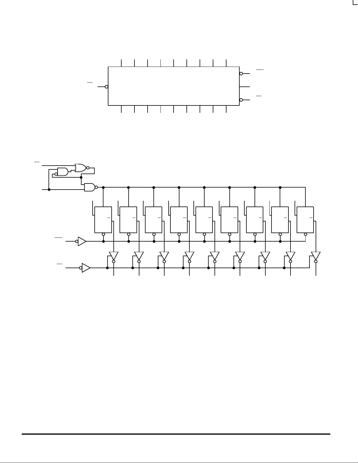
The MC74AC/ACT823 consists of nine D-type edge-triggered flip-flops. This
device has 3-state outputs for bus systems, organized in a broadside pinning. In
addition to the clock and output enabled pins, the buffered clock (CP) and buffered
Output Enable (OE
) are common to all flip-flips. The flip-flops will store the state of
their individual D inputs that meet the setup and hold time requirements on the
LOW-to-HIGH CP transition. With OE
LOW, the contents of the flip-flops are available
at the outputs. When OE
is HIGH, the outputs go to the high impedance state.
Operation of the OE
input does not affect the state of the flip-flops. The
MC74AC/ACT823 has Clear (CLR
) and Clock Enable (EN) pins. These devices are
ideal for parity bus interfacing in high performance systems.
When CLR
is LOW, and OE is LOW, the outputs are LOW. When CLR is HIGH,
data can be entered into the flip-flops. When EN
is LOW, data on the inputs is
transferred to the outputs on the LOW-to-HIGH clock transition. When EN
is HIGH,
the outputs do not change state, regardless of the data or clock input transitions.
• 3-State Outputs for Bus Interfacing
• Broad Side Pin Configuration
• ACT has TTL – Compatible Inputs
• High Speed Parallel Positive Edge-Triggered D-Type Flip-Flops
• High Performance Bus Interface Buffering for Busses Carrying Parity
• Outputs Source/Sink 24 mA
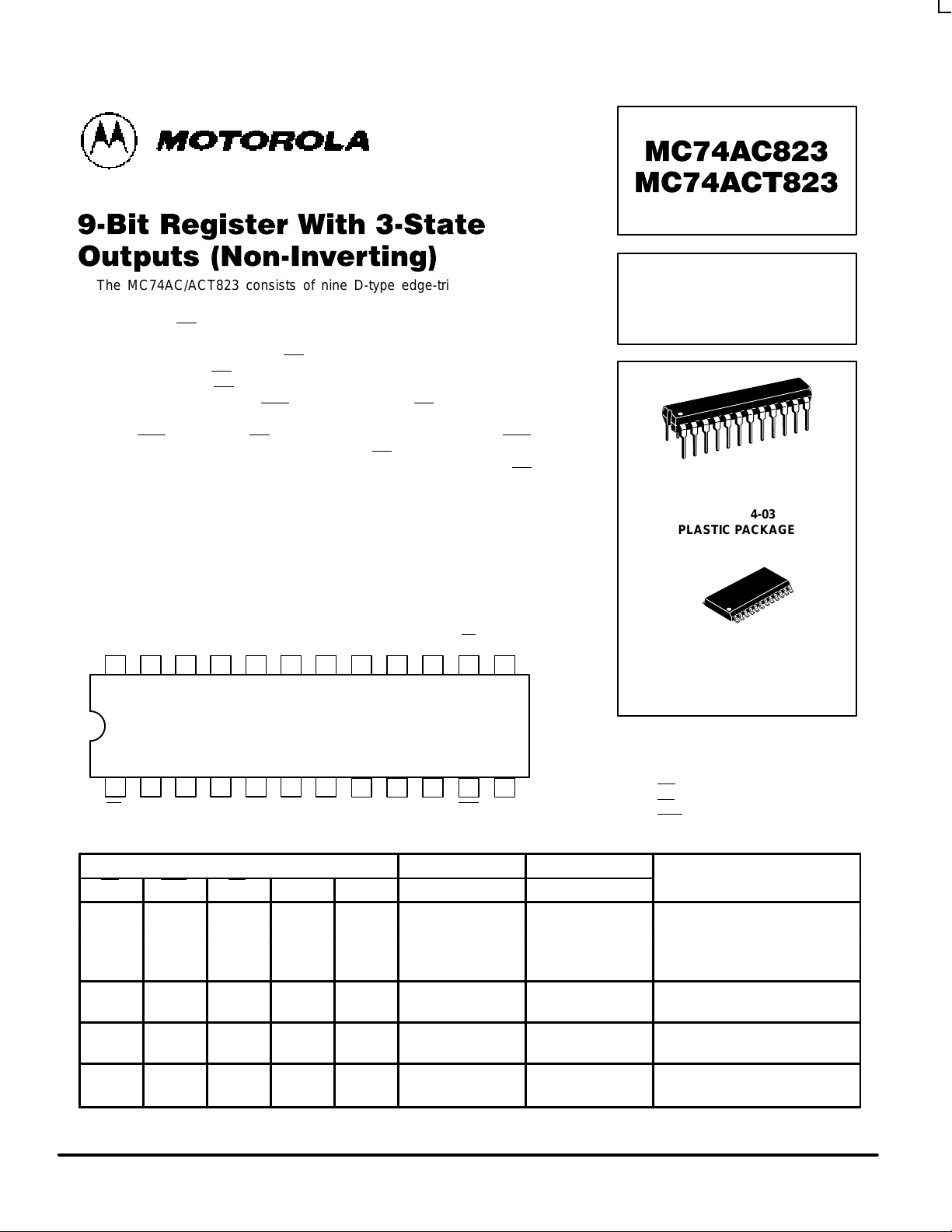
Pinout: 24-Lead Packages (Top View)
2324 22 21 20 19 18
V
CC
17
O0O1O2O3O4O5O
6
21 3 4 5 6 7
8
OE
1D0D1D2D3D4D5D6
16
9
O
7
D
7
15
10
O
8
D
8
14
11
EN
CLR
13
12
CP
GND
FUNCTION TABLE
Inputs Internal Outputs
OE CLR EN CP Dn Q O
Operating Mode
H X L ↑ L L Z High Z
H X L ↑ H H Z High Z
H L X X X L Z Clear
L L X X X L L Clear
H H H X X NC Z Hold
L H H X X NC NC Hold
H H L ↑ L L Z Load
H H L ↑ H H Z Load
L H L ↑ L L L Load
L H L ↑ H H H Load
H = HIGH Voltage Level; L = LOW Voltage Level; X = Immaterial; Z = High Impedance State; ↑ = LOW-to-High Transition; NC = No Change
This document contains information on a product under development. Motorola reserves the right to change or discontinue this product without notice.
9-BIT REGISTER WITH
3-STATE OUTPUTS
N SUFFIX
CASE 724-03
PLASTIC PACKAGE
1
24
PIN NAMES
Data Inputs
Data Outputs
Output Enable
Clock Enable
Clear
Clock Input
D0 – D
8
O0 – O
8
OE
EN
CLR
CP
DW SUFFIX
CASE 751E-04
SOIC PACKAGE
Page 2
MC74AC823 MC74ACT823
5-2
FACT DATA
LOGIC SYMBOL
O0O1O2O3O4O5O
6
D0D1D2D3D4D5D
6
O
7
D
7
O
8
D
8
CLR
CP
EN
OE
Q
D
CP
D
0
Q
0
CLR
OE
EN
CP
CLR
Q
D
CP
D
1
Q
1
CLR
Q
D
CP
D
2
Q
2
CLR
Q
D
CP
D
3
Q
3
CLR
Q
D
CP
D
4
Q
4
CLR
Q
D
CP
D
5
Q
5
CLR
Q
D
CP
D
6
Q
6
CLR
Q
D
CP
D
7
Q
7
CLR
Q
D
CP
D
8
Q
8
CLR
LOGIC DIAGRAM
Page 3
MC74AC823 MC74ACT823
5-3
FACT DATA
MAXIMUM RATINGS*
Symbol Parameter Value Units
V
CC
DC Supply Voltage (Referenced to GND) –0.5 to +7.0 V
V
in
DC Input Voltage (Referenced to GND) –0.5 to VCC + 0.5 V
V
O
DC Output Voltage (Referenced to GND) –0.5 to VCC + 0.5 V
I
in
DC Input Current, per Pin ± 20 mA
I
out
DC Output Sink/Source Current, per Pin ± 50 mA
I
CC
DC VCC or GND Current per Output Pin ± 50 mA
T
stg
Storage Temperature Range –65 to +150 °C
* Maximum Ratings are those values beyond which damage to the device may occur. Functional operation should be restricted to the Recommended
Operating Conditions.
RECOMMENDED OPERATING CONDITIONS
Symbol Parameter Min Typ Min Unit
′AC 2.0 5.0 6.0
VCCSupply Voltage
′ACT 4.5 5.0 5.5
V
V
in
DC Input Voltage, Output Voltage (Ref. to GND) 0 V
CC
V
VCC @ 3.0 V 150
∆t/∆ v
Input Rise and Fall Time (Note 1)
′AC Devices except Schmitt Inputs
VCC @ 4.5 V 40 ns/V
′AC Devices except Schmitt Inputs
VCC @ 5.5 V 25
VCC @ 4.5 V 10
tr, t
f
Input Rise and Fall Time (Note 2)
′ACT Devices except Schmitt Inputs
VCC @ 5.5 V 8.0
ns/V
T
J
Junction Temperature (PDIP) 140 °C
T
A
Operating Ambient Temperature Range –40 25 85 °C
I
OH
Output Current — HIGH –24 mA
I
OL
Output Current — LOW 24 mA
1. Vin from 30% to 70% VCC; see individual Data Sheets for devices that differ from the typical input rise and fall times.
2. Vin from 0.8 V to 2.0 V; see individual Data Sheets for devices that differ from the typical input rise and fall times.
Input Rise and Fall Time (Note 2)
Page 4

MC74AC823 MC74ACT823
5-4
FACT DATA
DC CHARACTERISTICS
74AC 74AC
Symbol
Parameter
V
CC
(V)
TA = +25°C
TA =
–40°C to +85°C
Unit
Conditions
Typ Guaranteed Limits
V
IH
3.0 1.5 2.1 2.1 V
OUT
= 0.1 V
4.5 2.25 3.15 3.15 V or VCC – 0.1 V
5.5 2.75 3.85 3.85
V
IL
3.0 1.5 0.9 0.9 V
OUT
= 0.1 V
4.5 2.25 1.35 1.35 V or VCC – 0.1 V
5.5 2.75 1.65 1.65
V
OH
3.0 2.99 2.9 2.9 I
OUT
= – 50 µA
4.5 4.49 4.4 4.4 V
5.5 5.49 5.4 5.4
*VIN = VIL or V
IH
3.0 2.56 2.46
– 12 mA
4.5 3.86 3.76
V
I
OH
– 24 mA
5.5 4.86 4.76 – 24 mA
V
OL
3.0 0.002 0.1 0.1 I
OUT
= 50 µA
4.5 0.001 0.1 0.1 V
5.5 0.001 0.1 0.1
*VIN = VIL or V
IH
3.0 0.36 0.44
12 mA
4.5 0.36 0.44
V
I
OH
24 mA
5.5 0.36 0.44 24 mA
I
IN
5.5
±0.1
±1.0
µA
I
= VCC, GND
I
OZ
VI (OE) = VIL, V
IH
5.5 ±0.5 ±5.0 µA VI = VCC, GND
VO = VCC, GND
I
OLD
5.5 75 mA V
OLD
= 1.65 V Max
I
OHD
Output Current
5.5 –75 mA V
OHD
= 3.85 V Min
I
CC
5.5
8.080µA
IN
= VCC or GND
* All outputs loaded; thresholds on input associated with output under test.
†Maximum test duration 2.0 ms, one input loaded at a time.
Note: IIN and ICC @ 3.0 V are guaranteed to be less than or equal to the respective limit @ 5.5 V VCC.
Minimum High Level
Input Voltage
Maximum Low Level
Input Voltage
Minimum High Level
Output Voltage
Maximum Low Level
Output Voltage
Maximum Input
Leakage Current
VI = VCC, GND
Maximum
3-State Current
†Minimum Dynamic
Maximum Quiescent
Supply Current
VIN = VCC or GND
Page 5

MC74AC823 MC74ACT823
5-5
FACT DATA
AC CHARACTERISTICS
74AC 74AC
Symbol
Parameter
VCC*
(V)
TA = +25°C
CL = 50 pF
TA = –40°C
to +85°C
CL = 50 pF
Unit
Fig.
No.
Min Typ Max Min Max
3.3
f
max
5.0
MHz
3.3
t
PLH
5.0
ns
3.3
t
PHL
5.0
ns
3.3
t
PHL
to O
n
5.0
ns
3.3
t
PZH
to O
n
5.0
ns
3.3
t
PZL
to O
n
5.0
ns
3.3
t
PHZ
to O
n
5.0
ns
3.3
t
PLZ
to O
n
5.0
ns
* Voltage Range 3.3 V is 3.3 V ±0.3 V.
Voltage Range 5.0 V is 5.0 V ±0.5 V.
AC OPERATING REQUIREMENTS
74AC 74AC
Symbol
Parameter
VCC*
(V)
TA = +25°C
CL = 50 pF
TA = –40°C
to +85°C
CL = 50 pF
Unit
Fig.
No.
Typ Guaranteed Minimum
Set-up Time, HIGH or LOW 3.3
t
s
Dn to CP 5.0
ns
Hold Time, HIGH or LOW 3.3
t
h
Dn to CP 5.0
ns
Set-up Time, HIGH or LOW 3.3
t
s
EN to CP 5.0
ns
Hold Time, HIGH or LOW 3.3
t
h
EN to CP 5.0
ns
CP Pulse Width 3.3
t
w
HIGH or LOW 5.0
ns
CLR Pulse Width, LOW 3.3
t
w
5.0
ns
CLR to CP 3.3
t
rec
Recovery Time 5.0
ns
* Voltage Range 3.3 V is 3.3 V ±0.3 V.
Voltage Range 5.0 V is 5.0 V ±0.5 V.
Maximum Clock
Frequency
Propagation Delay
CP to Q
n
Propagation Delay
CP to Q
n
Propagation Delay
CLR
Output Enable Time
OE
Output Enable Time
OE
Output Disable Time
OE
Output Disable Time
OE
Page 6

MC74AC823 MC74ACT823
5-6
FACT DATA
DC CHARACTERISTICS
74ACT 74ACT
Symbol
Parameter
V
CC
(V)
TA = +25°C
TA =
–40°C to +85°C
Unit
Conditions
Typ Guaranteed Limits
V
IH
4.5 1.5 2.0 2.0
V
OUT
= 0.1 V
5.5 1.5 2.0 2.0
V
or VCC – 0.1 V
V
IL
4.5 1.5 0.8 0.8
V
OUT
= 0.1 V
5.5 1.5 0.8 0.8
V
or VCC – 0.1 V
V
OH
4.5 4.49 4.4 4.4
I
OUT
= – 50 µA
5.5 5.49 5.4 5.4
V
*VIN = VIL or V
IH
4.5 3.86 3.76 V
– 24 mA
5.5 4.86 4.76
I
OH
– 24 mA
V
OL
4.5 0.001 0.1 0.1
I
OUT
= 50 µA
5.5 0.001 0.1 0.1
V
*VIN = VIL or V
IH
4.5 0.36 0.44 V
24 mA
5.5 0.36 0.44
I
OH
24 mA
I
IN
5.5
±0.1
±1.0
µA
VI = VCC, GND
I
OZ
VI (OE) = VIL, V
IH
5.5 ±0.5 ±5.0 µA VI = VCC, GND
VO = VCC, GND
∆I
CCT
Additional Max. ICC/Input 5.5 0.6 1.5
I
OLD
5.5 75 mA V
OLD
= 1.65 V Max
I
OHD
Output Current
5.5 –75 mA V
OHD
= 3.85 V Min
I
CC
5.5
8.080µA
IN
= VCC or GND
* All outputs loaded; thresholds on input associated with output under test.
†Maximum test duration 2.0 ms, one input loaded at a time.
Minimum High Level
Input Voltage
Maximum Low Level
Input Voltage
Minimum High Level
Output Voltage
Maximum Low Level
Output Voltage
Maximum Input
Leakage Current
Maximum
3-State Current
†Minimum Dynamic
Maximum Quiescent
Supply Current
VIN = VCC or GND
Page 7

MC74AC823 MC74ACT823
5-7
FACT DATA
AC CHARACTERISTICS (For Figures and Waveforms — See Section 3)
74ACT 74ACT
Symbol
Parameter
VCC*
(V)
TA = +25°C
CL = 50 pF
TA = –40°C
to +85°C
CL = 50 pF
Unit
Fig.
No.
Min Typ Max Min Max
f
max
5.0
120
158
109
MHz
t
PLH
5.0
1.5
5.5
9.5
1.5
10.5
ns
t
PHL
5.0
2.0
5.5
9.5
1.5
10.5
ns
t
PHL
to O
n
5.0
2.5
8.0
13.5
2.0
15.5
ns
t
PZH
to O
n
5.0
1.5
6.0
10.5
1.5
11.5
ns
t
PZL
to O
n
5.0
2.0
6.5
11.0
1.5
12.0
ns
t
PHZ
to O
n
5.0
1.5
6.5
11.0
1.5
12.0
ns
t
PLZ
to O
n
5.0
1.5
6.0
10.5
1.5
11.5
ns
* Voltage Range 5.0 V is 5.0 V ±0.5 V.
AC OPERATING REQUIREMENTS
74ACT 74ACT
Symbol
Parameter
VCC*
(V)
TA = +25°C
CL = 50 pF
TA = –40°C
to +85°C
CL = 50 pF
Unit
Fig.
No.
Typ Guaranteed Minimum
Set-up Time, HIGH or LOW
t
s
Dn to CP
5.0
0.5
2.5
2.5
ns
Hold Time, HIGH or LOW
t
h
Dn to CP
5.002.5
2.5
ns
Set-up Time, HIGH or LOW
t
s
EN to CP
5.002.0
2.5
ns
Hold Time, HIGH or LOW
t
h
EN to CP
5.001.0
1.0
ns
CP Pulse Width,
t
w
HIGH or LOW
5.0
2.5
4.5
5.5
ns
CLR Pulse Width,
t
w
LOW
5.0
3.0
5.5
5.5
ns
CLR to CP
t
rec
Recovery TIme
5.0
1.5
3.5
4.0
ns
* Voltage Range 5.0 V is 5.0 V ±0.5 V.
CAPACITANCE
Symbol Parameter
Value
Typ
Unit Test Conditions
C
IN
Input Capacitance 4.5 pF VCC = 5.0 V
C
PD
Power Dissipation Capacitance 44.0 pF VCC = 5.0 V
Maximum Clock
Frequency
Propagation Delay
CP to Q
n
Propagation Delay
CP to Q
n
Propagation Delay
CLR
Output Enable Time
OE
Output Enable Time
OE
Output Disable Time
OE
Output Disable Time
OE
Page 8

MC74AC823 MC74ACT823
5-8
FACT DATA
OUTLINE DIMENSIONS
N SUFFIX
PLASTIC DIP PACKAGE
CASE 724–03
ISSUE D
DW SUFFIX
PLASTIC SOIC PACKAGE
CASE 751E–04
ISSUE E
NOTES:
1. DIMENSIONING AND TOLERANCING PER
ANSI Y14.5M, 1982.
2. CONTROLLING DIMENSION: MILLIMETER.
3. DIMENSIONS A AND B DO NOT INCLUDE
MOLD PROTRUSION.
4. MAXIMUM MOLD PROTRUSION 0.15 (0.006)
PER SIDE.
5. DIMENSION D DOES NOT INCLUDE DAMBAR
PROTRUSION. ALLOWABLE DAMBAR
PROTRUSION SHALL BE 0.13 (0.005) TOTAL IN
EXCESS OF D DIMENSION AT MAXIMUM
MATERIAL CONDITION.
–A–
–B– P12X
D24X
12
1324
1
M
0.010 (0.25) B
M
S
A
M
0.010 (0.25) B
S
T
–T–
G
22X
SEATING
PLANE
K
C
R
X 45
_
M
F
J
DIM MIN MAX MIN MAX
INCHESMILLIMETERS
A 15.25 15.54 0.601 0.612
B 7.40 7.60 0.292 0.299
C 2.35 2.65 0.093 0.104
D 0.35 0.49 0.014 0.019
F 0.41 0.90 0.016 0.035
G 1.27 BSC 0.050 BSC
J 0.23 0.32 0.009 0.013
K 0.13 0.29 0.005 0.011
M 0 8 0 8
P 10.05 10.55 0.395 0.415
R 0.25 0.75 0.010 0.029
____
NOTES:
1. CHAMFERED CONTOUR OPTIONAL.
2. DIMENSION L TO CENTER OF LEADS WHEN
FORMED PARALLEL.
3. DIMENSIONING AND TOLERANCING PER ANSI
Y14.5M, 1982.
4. CONTROLLING DIMENSION: INCH.
–A–
–B–
24 13
12
1
–T–
SEATING
PLANE
24 PL
K
E
F
N
C
D
G
M
A
M
0.25 (0.010) T
24 PLJ
M
B
M
0.25 (0.010) T
L
M
NOTE 1
DIM MIN MAX MIN MAX
MILLIMETERSINCHES
A 1.230 1.265 31.25 32.13
B 0.250 0.270 6.35 6.85
C 0.145 0.175 3.69 4.44
D 0.015 0.020 0.38 0.51
E 0.050 BSC 1.27 BSC
F 0.040 0.060 1.02 1.52
G 0.100 BSC 2.54 BSC
J 0.007 0.012 0.18 0.30
K 0.110 0.140 2.80 3.55
L 0.300 BSC 7.62 BSC
M 0 15 0 15
N 0.020 0.040 0.51 1.01
_ _ _ _
How to reach us:
USA/EUROPE: Motorola Literature Distribution; JAPAN: Nippon Motorola Ltd.; Tatsumi–SPD–JLDC, Toshikatsu Otsuki,
P.O. Box 20912; Phoenix, Arizona 85036. 1–800–441–2447 6F Seibu–Butsuryu–Center, 3–14–2 Tatsumi Koto–Ku, Tokyo 135, Japan. 03–3521–8315
MFAX: RMFAX0@email.sps.mot.com –TOUCHTONE (602) 244–6609 HONG KONG: Motorola Semiconductors H.K. Ltd.; 8B Tai Ping Industrial Park,
INTERNET: http://Design–NET.com 51 Ting Kok Road, Tai Po, N.T., Hong Kong. 852–26629298
Motorola reserves the right to make changes without further notice to any products herein. Motorola makes no warranty , representation or guarantee regarding
the suitability of its products for any particular purpose, nor does Motorola assume any liability arising out of the application or use of any product or circuit, and
specifically disclaims any and all liability , including without limitation consequential or incidental damages. “Typical” parameters can and do vary in different
applications. All operating parameters, including “T ypicals” must be validated for each customer application by customer’s technical experts. Motorola does
not convey any license under its patent rights nor the rights of others. Motorola products are not designed, intended, or authorized for use as components in
systems intended for surgical implant into the body, or other applications intended to support or sustain life, or for any other application in which the failure of
the Motorola product could create a situation where personal injury or death may occur. Should Buyer purchase or use Motorola products for any such
unintended or unauthorized application, Buyer shall indemnify and hold Motorola and its officers, employees, subsidiaries, affiliates, and distributors harmless
against all claims, costs, damages, and expenses, and reasonable attorney fees arising out of, directly or indirectly, any claim of personal injury or death
associated with such unintended or unauthorized use, even if such claim alleges that Motorola was negligent regarding the design or manufacture of the part.
Motorola and are registered trademarks of Motorola, Inc. Motorola, Inc. is an Equal Opportunity/Affirmative Action Employer.
MC74AC823/D
*MC74AC823/D*
◊
 Loading...