

Datasheet MC74ACT646DWR2, MC74ACT646DW, MC74AC646N, MC74AC646DW, MC74AC646DWR2 Datasheet (Motorola)
...Page 1
5-1
FACT DATA
! !
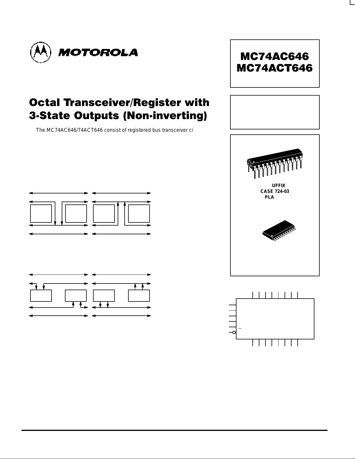
The MC74AC646/74ACT646 consist of registered bus transceiver circuits,
with outputs, D-type flip-flops and control circuitry providing multiplexed transmission
of data directly from the input bus or from the internal storage registers. Data on the
A or B bus will be loaded into the respective registers on the LOW-to-HIGH transition
of the appropriate clock pin (CAB or CBA). The four fundamental data handling
functions available are illustrated in the following figures.
REAL TIME TRANSFER
A-BUS TO B-BUS
REAL TIME TRANSFER
B-BUS TO A-BUS
REG
REG REG REG
REG REG REG REG
B-BUS B-BUS
A-BUS A-BUS
B-BUS B-BUS
A-BUS A-BUS
STORAGE
FROM BUS TO REGISTER
TRANSFER
FROM REGISTER TO BUS
Figure 1 Figure 2
Figure 3 Figure 4
• Independent Registers for A and B Buses
• Multiplexed Real-Time and Stored Data Transfers
• Choice of True and Inverting Data Paths
• 3-State Outputs
• 300 mil Slim Dual In-Line Package
• Outputs Source/Sink 24 mA
• ′ACT646 Has TTL Compatible Inputs
OCTAL
TRANSCEIVER/REGISTER
WITH 3-STATE OUTPUTS
(NON-INVERTING)
N SUFFIX
CASE 724-03
PLASTIC
DW SUFFIX
CASE 751E-04
SOIC PACKAGE
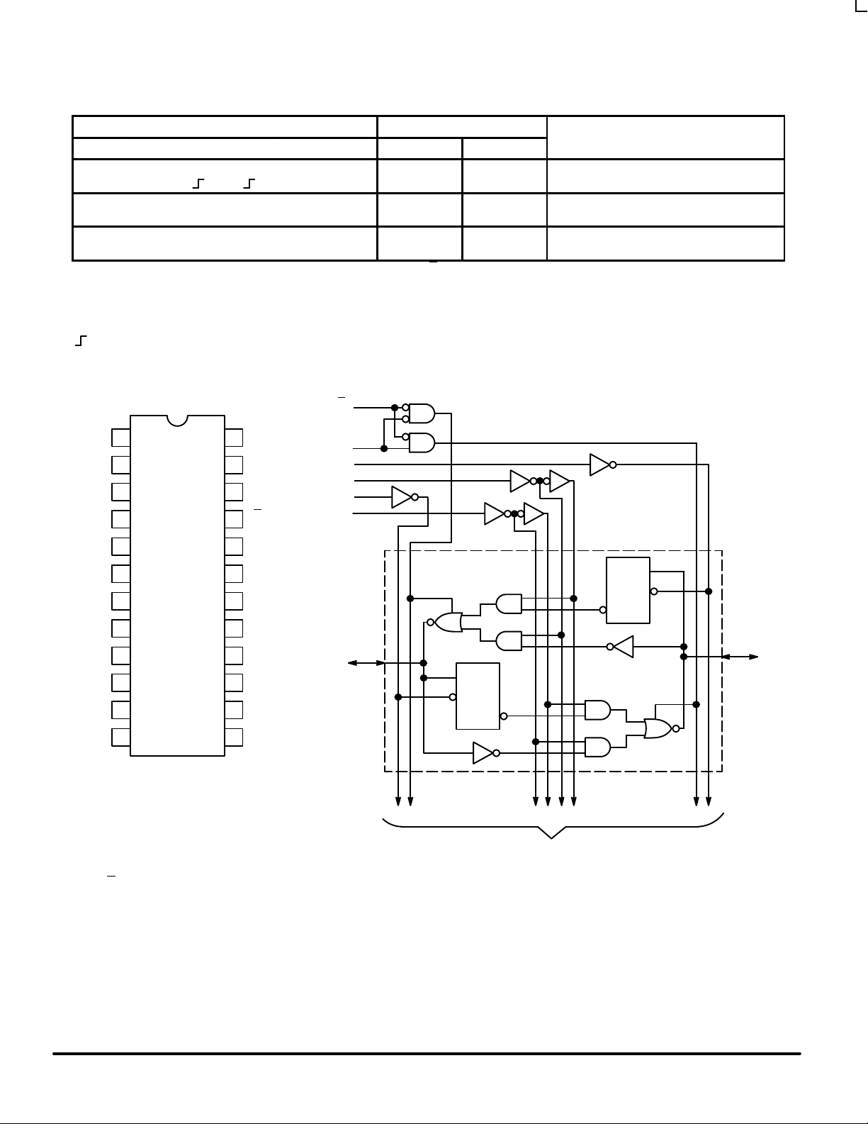
LOGIC SYMBOL
A0A1A2A3A4A5A6A
7
B0B1B2B3B4B5B6B
7
CAB
SAB
DIR
CBA
SBA
G
Page 2
MC74AC646 MC74ACT646
5-2
FACT DATA
FUNCTION TABLE
Inputs Data I/O*
G DIR CAB CBA SAB SBA A0–A
7
B0–B
7
Operation or Function
H
H
X
X
H or L H or L X
X
X
X
Input Input
Isolation
Store A and B Data
L
L
L
L
X
X
X
X
X
X
L
H
Output Input
Real Time B Data to A Bus
Stored B Data to A Bus
L
L
H
H
X
H or L
X
X
L
H
X
X
Input Output
Real Time A Data to B Bus
Stored A Data to B Bus
* The data output functions may be enabled or disabled by various signals at the G and DIR inputs. Data input functions are always enabled; i.e., data at the bus
pins will be stored on every LOW-to-HIGH transition of the appropriate clock inputs.
H = HIGH Voltage Level
L = LOW Voltage Level
X = Immaterial
= LOW-to-HIGH Transition
1 OF 8 CHANNELS
D
0
C
0
D
0
C
0
CAB
SAB
DIR
CBA
SBA
G
B
0
A
0
TO 7 OTHER CHANNELS
LOGIC DIAGRAM
Please note that this diagram is provided only for the understanding of logic
operations and should not be used to estimate propagation delays.
1
CAB
2
SAB
3
DIR
4
A
0
5
A
1
6
A
2
7
A
3
8
A
4
9
A
5
10
A
6
11
A
7
12
GND
24
23
22
21
20
19
18
17
16
14
13
V
CC
CBA
SBA
G
B
0
B
1
B
2
B
3
B
4
B
5
B
6
B
7
PIN NAMES
A0–A7 Data Register Inputs
Data Register A Outputs
B0–B
7
Data Register B Inputs
Data Register B Outputs
CAB, CBA Clock Pulse Inputs
SAB, SBA Transmit/Receive Inputs
DIR, G
Output Enable Inputs
15
Page 3
MC74AC646 MC74ACT646
5-3
FACT DATA
MAXIMUM RATINGS*
Symbol Parameter Value Unit
V
CC
DC Supply Voltage (Referenced to GND) –0.5 to +7.0 V
V
in
DC Input Voltage (Referenced to GND) –0.5 to VCC +0.5 V
V
out
DC Output Voltage (Referenced to GND) –0.5 to VCC +0.5 V
I
in
DC Input Current, per Pin ±20 mA
I
out
DC Output Sink/Source Current, per Pin ±50 mA
I
CC
DC VCC or GND Current per Output Pin ±50 mA
T
stg
Storage Temperature –65 to +150 °C
* Maximum Ratings are those values beyond which damage to the device may occur. Functional operation should be restricted to the Recommended
Operating Conditions.
RECOMMENDED OPERATING CONDITIONS
Symbol Parameter Min Typ Max Unit
′AC 2.0 5.0 6.0
VCCSupply Voltage
′ACT 4.5 5.0 5.5
V
Vin, V
out
DC Input Voltage, Output Voltage (Ref. to GND) 0 V
CC
V
VCC @ 3.0 V 150
Input Rise and Fall Time (Note 1)
′AC Devices except Schmitt Inputs
VCC @ 4.5 V 40 ns/V
r
, t
f
′AC Devices except Schmitt Inputs
VCC @ 5.5 V 25
VCC @ 4.5 V 10
tr, t
f
Input Rise and Fall Time (Note 2)
′ACT Devices except Schmitt Inputs
VCC @ 5.5 V 8.0
ns/V
T
J
Junction Temperature (PDIP) 140 °C
T
A
Operating Ambient Temperature Range –40 25 85 °C
I
OH
Output Current — High –24 mA
I
OL
Output Current — Low 24 mA
1. Vin from 30% to 70% VCC; see individual Data Sheets for devices that differ from the typical input rise and fall times.
2. Vin from 0.8 V to 2.0 V; see individual Data Sheets for devices that differ from the typical input rise and fall times.
tr, t
f
Input Rise and Fall Time (Note 2)
Page 4

MC74AC646 MC74ACT646
5-4
FACT DATA
DC CHARACTERISTICS
74AC 74AC
Symbol
Parameter
V
CC
(V)
TA = +25°C
TA =
–40°C to +85°C
Unit
Conditions
Typ Guaranteed Limits
V
IH
3.0 1.5 2.1 2.1 V
OUT
= 0.1 V
4.5 2.25 3.15 3.15 V or VCC – 0.1 V
5.5 2.75 3.85 3.85
V
IL
3.0 1.5 0.9 0.9 V
OUT
= 0.1 V
4.5 2.25 1.35 1.35 V or VCC – 0.1 V
5.5 2.75 1.65 1.65
V
OH
3.0 2.99 2.9 2.9 I
OUT
= –50 µA
4.5 4.49 4.4 4.4 V
5.5 5.49 5.4 5.4
*VIN = VIL or V
IH
3.0 2.56 2.46
–12 mA
4.5 3.86 3.76
V
I
OH
–24 mA
5.5 4.86 4.76 –24 mA
V
OL
3.0 0.002 0.1 0.1 I
OUT
= 50 µA
4.5 0.001 0.1 0.1 V
5.5 0.001 0.1 0.1
*VIN = VIL or V
IH
3.0 0.36 0.44
12 mA
4.5 0.36 0.44
V
I
OL
24 mA
5.5 0.36 0.44 24 mA
I
IN
5.5
±0.1
±1.0
µA
VI = VCC, GND
I
OZT
VI (OE) = VIL, V
IH
5.5 ±0.6 ±6.0 µA VI = VCC, GND
VO = VCC, GND
I
OLD
5.5 75 mA V
OLD
= 1.65 V Max
I
OHD
Output Current
5.5 –75 mA V
OHD
= 3.85 V Min
I
CC
5.5
8.080µA
VIN = VCC or GND
* All outputs loaded; thresholds on input associated with output under test.
†Maximum test duration 2.0 ms, one output loaded at a time.
Note: IIN and ICC @ 3.0 V are guaranteed to be less than or equal to the respective limit @ 5.5 V VCC.
Minimum High Level
Input Voltage
Maximum Low Level
Input Voltage
Minimum High Level
Output Voltage
Maximum Low Level
Output Voltage
Maximum Input
Leakage Current
Maximum
3-State
Current
†Minimum Dynamic
Maximum Quiescent
Supply Current
Page 5

MC74AC646 MC74ACT646
5-5
FACT DATA
AC CHARACTERISTICS (For Figures and Waveforms — See Section 3)
74AC 74AC
Symbol
Parameter
VCC*
(V)
TA = +25°C
CL = 50 pF
TA = –40°C
to +85°C
CL = 50 pF
Unit
Fig.
No.
Min Typ Max Min Max
Propagation Delay
3.3 4.0 10.5 16.5 3.0 18.5
t
PLH
Clock to Bus 5.0 2.5 7.5 12 2.0 13
ns
3-6
Propagation Delay
3.3 3.0 9.5 14.5 2.5 16
t
PHL
Clock to Bus 5.0 2.0 6.5 10.5 1.5 11.5
ns
3-6
Propagation Delay
3.3 2.5 7.5 12 2.0 13.5
t
PLH
Bus to Bus 5.0 1.5 5.0 8.0 1.0 9.0
ns
3-5
Propagation Delay
3.3 1.5 7.5 12.5 1.5 13.5
t
PHL
Bus to Bus 5.0 1.5 5.0 9.0 1.0 9.5
ns
3-5
Propagation Delay
SBA or SAB to An or B
n
(w/An or Bn HIGH or LOW)
3.3
5.0
2.0
1.5
8.5
6.0
13.5101.5
1.5
15.5
11
Propagation Delay
SBA or SAB to An or B
n
(w/An or Bn HIGH or LOW)
3.3
5.0
1.5
1.5
8.5
6.0
13.5101.5
1.51511
3.3 2.5 7.0 11.5 2.0 12.5
t
PZH
to An or B
n
5.0 1.5 5.0 8.5 1.5 9.0
ns
3-7
3.3 2.5 7.5 12.5 2.0 14
t
PZL
to An or B
n
5.0 1.5 5.5 9.0 1.5 10
ns
3-8
3.3 3.0 8.0 12.5 2.5 13.5
t
PHZ
to An or B
n
5.0 2.0 6.5 10 2.0 11
ns
3-7
3.3 2.0 7.5 12 2.0 13.5
t
PLZ
to An or B
n
5.0 1.5 6.0 9.5 1.5 10.5
ns
3-8
3.3 2.0 6.5 11 1.5 12
t
PZH
5.0 1.5 5.0 7.5 1.0 8.5
ns
3-7
3.3 2.5 7.0 11.5 2.0 13
t
PZL
5.0 1.5 5.0 8.0 1.0 9.0
ns
3-8
3.3 2.5 7.5 11.5 1.5 12.5
t
PHZ
5.0 1.5 5.5 9.5 1.5 10
ns
3-7
3.3 1.5 7.5 12 1.5 13.5
t
PLZ
5.0 1.5 5.5 9.5 1.5 10.5
ns
3-8
* Voltage Range 3.3 V is 3.3 V ±0.3 V.
Voltage Range 5.0 V is 5.0 V ±0.5 V.
t
PLH
t
PHL
Enable Time
G
Enable Time
G
Disable Time
G
Disable Time
G
Enable Time
DIR to An or B
Enable Time
DIR to An or B
Disable Time
DIR to An or B
Disable Time
DIR to An or B
n
n
n
n
ns 3-6
ns 3-6
Page 6

MC74AC646 MC74ACT646
5-6
FACT DATA
AC OPERATING REQUIREMENTS
74AC 74AC
Symbol
Parameter
VCC*
(V)
TA = +25°C
CL = 50 pF
TA = –40°C
to +85°C
CL = 50 pF
Unit
Fig.
No.
Typ Guaranteed Minimum
Setup Time, HIGH or LOW 3.3 2.0 5.0 5.5
t
s
Bus to Clock 5.0 1.5 4.0 4.5
ns
3-9
Hold Time, HIGH or LOW 3.3 –1.5 0 0
t
h
Bus to Clock 5.0 –0.5 0.5 1.0
ns
3-9
Clock Pulse Width 3.3 2.0 3.5 4.5
t
w
HIGH or LOW 5.0 2.0 3.5 3.5
ns
3-6
* Voltage Range 3.3 V is 3.3 V ±0.3 V.
Voltage Range 5.0 V is 5.0 V ±0.5 V.
DC CHARACTERISTICS
74ACT 74ACT
Symbol
Parameter
V
CC
(V)
TA = +25°C
TA =
–40°C to +85°C
Unit
Conditions
Typ Guaranteed Limits
V
IH
4.5 1.5 2.0 2.0
V
OUT
= 0.1 V
5.5 1.5 2.0 2.0
V
or VCC – 0.1 V
V
IL
4.5 1.5 0.8 0.8
V
OUT
= 0.1 V
5.5 1.5 0.8 0.8
V
or VCC – 0.1 V
V
OH
4.5 4.49 4.4 4.4
I
OUT
= –50 µA
5.5 5.49 5.4 5.4
V
*VIN = VIL or V
IH
4.5 3.86 3.76 V
–24 mA
5.5 4.86 4.76
I
OH
–24 mA
V
OL
4.5 0.001 0.1 0.1
I
OUT
= 50 µA
5.5 0.001 0.1 0.1
V
*VIN = VIL or V
IH
4.5 0.36 0.44 V
24 mA
5.5 0.36 0.44
I
OL
24 mA
I
IN
5.5
±0.1
±1.0
µA
VI = VCC, GND
∆I
CCT
Additional Max. ICC/Input 5.5 0.6 1.5 mA VI = VCC – 2.1 V
I
OZT
VI (OE) = VIL, V
IH
5.5 ±0.6 ±6.0 µA VI = VCC, GND
VO = VCC, GND
I
OLD
5.5 75 mA V
OLD
= 1.65 V Max
I
OHD
Output Current
5.5 –75 mA V
OHD
= 3.85 V Min
I
CC
5.5
8.080µA
VIN = VCC or GND
* All outputs loaded; thresholds on input associated with output under test.
†Maximum test duration 2.0 ms, one output loaded at a time.
Minimum High Level
Input Voltage
Maximum Low Level
Input Voltage
Minimum High Level
Output Voltage
Maximum Low Level
Output Voltage
Maximum Input
Leakage Current
Maximum
3-State
Current
†Minimum Dynamic
Maximum Quiescent
Supply Current
Page 7

MC74AC646 MC74ACT646
5-7
FACT DATA
AC CHARACTERISTICS (For Figures and Waveforms — See Section 3)
74ACT 74ACT
Symbol
Parameter
VCC*
(V)
TA = +25°C
CL = 50 pF
TA = –40°C
to +85°C
CL = 50 pF
Unit
Fig.
No.
Min Typ Max Min Max
t
PLH
5.0
3.5
12.0
14.5
3.0
16.0ns3-6
t
PHL
5.0
4.0
12.0
14.5
3.5
16.0ns3-6
t
PLH
5.0
3.0
8.5
11.0
2.5
12.0ns3-5
t
PHL
5.0
2.5
8.5
11.0
2.0
12.0ns3-5
t
PLH
SBA or SAB to An or B
n
(w/An or Bn HIGH or LOW)
5.0
3.0
9.5
12.0
2.5
13.0ns3-6
t
PHL
SBA or SAB to An or B
n
(w/An or Bn HIGH or LOW)
5.0
3.0
9.5
12.0
2.5
13.0ns3-6
t
PZH
to An or B
n
5.0
2.0
9.0
11.0
1.5
12.0ns3-7
t
PZL
to An or B
n
5.0
3.5
9.0
11.0
3.0
12.0ns3-8
t
PHZ
to An or B
n
5.0
5.0
10.5
13.0
4.5
14.5ns3-7
t
PLZ
to An or B
n
5.0
3.5
10.0
12.5
3.0
14.0ns3-8
t
PZH
5.0
2.0
6.5
12.5
1.5
13.5ns3-7
t
PZL
5.0
3.5
6.5
12.5
3.0
13.5ns3-8
t
PHZ
5.0
5.0
8.5
12.5
4.5
13.5ns3-7
t
PLZ
5.0
3.5
8.5
12.5
3.0
13.5ns3-8
* Voltage Range 5.0 V is 5.0 V ±0.5 V.
Propagation Delay
Clock to Bus
Propagation Delay
Clock to Bus
Propagation Delay
Bus to Bus
Propagation Delay
Bus to Bus
Propagation Delay
Propagation Delay
Enable Time
G
Enable Time
G
Disable Time
G
Disable Time
G
Enable Time
DIR to An or B
Enable Time
DIR to An or B
Disable Time
DIR to An or B
Disable Time
DIR to An or B
n
n
n
n
Page 8

MC74AC646 MC74ACT646
5-8
FACT DATA
AC OPERATING REQUIREMENTS
74ACT 74ACT
Symbol
Parameter
VCC*
(V)
TA = +25°C
CL = 50 pF
TA = –40°C
to +85°C
CL = 50 pF
Unit
Fig.
No.
Typ Guaranteed Minimum
t
s
5.0
7.0
8.0
ns
3-9
t
h
5.0
2.5
2.5
ns
3-9
t
w
5.0
7.0
8.0
ns
3-6
* Voltage Range 5.0 V is 5.0 V ±0.5 V.
CAPACITANCE
Symbol Parameter
Value
Typ
Unit Test Conditions
C
IN
Input Capacitance 4.5 pF VCC = 5.0 V
C
I/O
Input/Output Capacitance 15 pF VCC = 5.0 V
C
PD
Power Dissipation Capacitance 60 pF VCC = 5.0 V
Setup Time, HIGH or LOW
Bus to Clock
Hold Time, HIGH or LOW
Bus to Clock
Clock Pulse Width
HIGH or LOW
Page 9

MC74AC646 MC74ACT646
5-9
FACT DATA
OUTLINE DIMENSIONS
N SUFFIX
PLASTIC DIP PACKAGE
CASE 724–03
ISSUE D
DW SUFFIX
PLASTIC SOIC PACKAGE
CASE 751E–04
ISSUE E
NOTES:
1. DIMENSIONING AND TOLERANCING PER
ANSI Y14.5M, 1982.
2. CONTROLLING DIMENSION: MILLIMETER.
3. DIMENSIONS A AND B DO NOT INCLUDE
MOLD PROTRUSION.
4. MAXIMUM MOLD PROTRUSION 0.15 (0.006)
PER SIDE.
5. DIMENSION D DOES NOT INCLUDE DAMBAR
PROTRUSION. ALLOWABLE DAMBAR
PROTRUSION SHALL BE 0.13 (0.005) TOTAL IN
EXCESS OF D DIMENSION AT MAXIMUM
MATERIAL CONDITION.
–A–
–B– P12X
D24X
12
1324
1
M
0.010 (0.25) B
M
S
A
M
0.010 (0.25) B
S
T
–T–
G
22X
SEATING
PLANE
K
C
R
X 45
_
M
F
J
DIM MIN MAX MIN MAX
INCHESMILLIMETERS
A 15.25 15.54 0.601 0.612
B 7.40 7.60 0.292 0.299
C 2.35 2.65 0.093 0.104
D 0.35 0.49 0.014 0.019
F 0.41 0.90 0.016 0.035
G 1.27 BSC 0.050 BSC
J 0.23 0.32 0.009 0.013
K 0.13 0.29 0.005 0.011
M 0 8 0 8
P 10.05 10.55 0.395 0.415
R 0.25 0.75 0.010 0.029
____
NOTES:
1. CHAMFERED CONTOUR OPTIONAL.
2. DIMENSION L TO CENTER OF LEADS WHEN
FORMED PARALLEL.
3. DIMENSIONING AND TOLERANCING PER ANSI
Y14.5M, 1982.
4. CONTROLLING DIMENSION: INCH.
–A–
–B–
24 13
12
1
–T–
SEATING
PLANE
24 PL
K
E
F
N
C
D
G
M
A
M
0.25 (0.010) T
24 PLJ
M
B
M
0.25 (0.010) T
L
M
NOTE 1
DIM MIN MAX MIN MAX
MILLIMETERSINCHES
A 1.230 1.265 31.25 32.13
B 0.250 0.270 6.35 6.85
C 0.145 0.175 3.69 4.44
D 0.015 0.020 0.38 0.51
E 0.050 BSC 1.27 BSC
F 0.040 0.060 1.02 1.52
G 0.100 BSC 2.54 BSC
J 0.007 0.012 0.18 0.30
K 0.110 0.140 2.80 3.55
L 0.300 BSC 7.62 BSC
M 0 15 0 15
N 0.020 0.040 0.51 1.01
_ _ _ _
How to reach us:
USA/EUROPE: Motorola Literature Distribution; JAPAN: Nippon Motorola Ltd.; Tatsumi–SPD–JLDC, Toshikatsu Otsuki,
P.O. Box 20912; Phoenix, Arizona 85036. 1–800–441–2447 6F Seibu–Butsuryu–Center, 3–14–2 Tatsumi Koto–Ku, Tokyo 135, Japan. 03–3521–8315
MFAX: RMFAX0@email.sps.mot.com –TOUCHTONE (602) 244–6609 HONG KONG: Motorola Semiconductors H.K. Ltd.; 8B Tai Ping Industrial Park,
INTERNET: http://Design–NET.com 51 Ting Kok Road, Tai Po, N.T., Hong Kong. 852–26629298
Motorola reserves the right to make changes without further notice to any products herein. Motorola makes no warranty , representation or guarantee regarding
the suitability of its products for any particular purpose, nor does Motorola assume any liability arising out of the application or use of any product or circuit, and
specifically disclaims any and all liability , including without limitation consequential or incidental damages. “Typical” parameters can and do vary in different
applications. All operating parameters, including “T ypicals” must be validated for each customer application by customer’s technical experts. Motorola does
not convey any license under its patent rights nor the rights of others. Motorola products are not designed, intended, or authorized for use as components in
systems intended for surgical implant into the body, or other applications intended to support or sustain life, or for any other application in which the failure of
the Motorola product could create a situation where personal injury or death may occur. Should Buyer purchase or use Motorola products for any such
unintended or unauthorized application, Buyer shall indemnify and hold Motorola and its officers, employees, subsidiaries, affiliates, and distributors harmless
against all claims, costs, damages, and expenses, and reasonable attorney fees arising out of, directly or indirectly, any claim of personal injury or death
associated with such unintended or unauthorized use, even if such claim alleges that Motorola was negligent regarding the design or manufacture of the part.
Motorola and are registered trademarks of Motorola, Inc. Motorola, Inc. is an Equal Opportunity/Affirmative Action Employer.
MC74AC646/D
*MC74AC646/D*
◊
 Loading...