

Datasheet MC68HSC705C8ACS, MC68HSC705C8ACFS, MC68HSC705C8ACFB, MC68HSC705C8ACFN, MC68HSC705C8AC Datasheet (Motorola)
...Page 1

MC68HC705C8A/D
Brought to you as a courtesy from Midon Design - home of the TEMP05
www.midondesign.com
Rev. 2.0
HC 5
MC68HC705C8A
MC68HSC705C8A
HCMOS Microcontroller Unit
TECHNICAL DATA
Page 2

Technical Data
Motorola reserves the right to make changes without further notice to
any products herein to improve reliability, function or design. Motorola
does not assume any liability arising out of the application or use of any
product or circuit described herein; neither does it convey any license
under its patent rights nor the rights of others. Motorola products are not
designed, intended, or authorized for use as components in systems
intendedfor surgical implant into thebody, or other applications intended
to support or sustain life, or for any other application in which the failure
of the Motorola product could create a situation where personal injury or
death may occur. Should Buyer purchase or use Motorola products for
any such unintended or unauthorized application, Buyer shall indemnify
and hold Motorola and its officers, employees, subsidiaries, affiliates,
and distributors harmless against all claims, costs, damages, and
expenses, and reasonable attorney fees arising out of, directly or
indirectly, any claim of personal injury or death associated with such
unintended or unauthorized use, evenif such claim alleges that Motorola
was negligent regarding the design or manufacture of the part.
© Motorola, Inc., 1999
NON-DISCLOSURE AGREEMENT REQUIRED
Technical Data MC68HC705C8A — Rev. 2.0
2 MOTOROLA
Page 3

Technical Data — MC68HC705C8A
Section 1. General Description . . . . . . . . . . . . . . . . . . . .19
Section 2. Memory . . . . . . . . . . . . . . . . . . . . . . . . . . . . . .33
Section 3. Central Processor Unit (CPU) . . . . . . . . . . . .41
Section 4. Interrupts . . . . . . . . . . . . . . . . . . . . . . . . . . . . .47
Section 5. Resets . . . . . . . . . . . . . . . . . . . . . . . . . . . . . . .59
Section 6. Low-Power Modes. . . . . . . . . . . . . . . . . . . . . .67
Section 7. Parallel Input/Output (I/O). . . . . . . . . . . . . . . .75
List of Sections
Section 8. Capture/Compare Timer . . . . . . . . . . . . . . . . .87
Section 9. EPROM/OTPROM (PROM) . . . . . . . . . . . . . .101
Section 10. Serial Communications Interface (SCI). . .119
Section 11. Serial Peripheral Interface (SPI). . . . . . . . .137
Section 12. Instruction Set. . . . . . . . . . . . . . . . . . . . . . .151
Section 13. Electrical Specifications . . . . . . . . . . . . . .169
Section 14. Mechanical Specifications . . . . . . . . . . . . .189
Section 15. Ordering Information . . . . . . . . . . . . . . . . .197
Appendix A. MC68HSC705C8A . . . . . . . . . . . . . . . . . . .199
MC68HC705C8A — Rev. 2.0 Technical Data
MOTOROLA List of Sections 3
Page 4

List of Sections
Technical Data MC68HC705C8A — Rev. 2.0
4 List of Sections MOTOROLA
Page 5

Technical Data — MC68HC705C8A
Section 1. General Description
1.1 Contents . . . . . . . . . . . . . . . . . . . . . . . . . . . . . . . . . . . . . . . . . .19
1.2 Introduction. . . . . . . . . . . . . . . . . . . . . . . . . . . . . . . . . . . . . . . .20
1.3 Features . . . . . . . . . . . . . . . . . . . . . . . . . . . . . . . . . . . . . . . . . .20
1.4 Programmable Options. . . . . . . . . . . . . . . . . . . . . . . . . . . . . . .21
1.5 Block Diagram . . . . . . . . . . . . . . . . . . . . . . . . . . . . . . . . . . . . .22
1.6 Pin Assignments. . . . . . . . . . . . . . . . . . . . . . . . . . . . . . . . . . . .24
1.7 Pin Functions . . . . . . . . . . . . . . . . . . . . . . . . . . . . . . . . . . . . . .27
1.7.1 V
1.7.2 OSC1 and OSC2 . . . . . . . . . . . . . . . . . . . . . . . . . . . . . . . . .27
1.7.3 External Reset Pin (
1.7.4 External Interrupt Request Pin (
1.7.5 Input Capture Pin (TCAP) . . . . . . . . . . . . . . . . . . . . . . . . . .30
1.7.6 Output Compare Pin (TCMP). . . . . . . . . . . . . . . . . . . . . . . .30
1.7.7 Port A I/O Pins (PA7–PA0). . . . . . . . . . . . . . . . . . . . . . . . . .30
1.7.8 Port B I/O Pins (PB7–PB0). . . . . . . . . . . . . . . . . . . . . . . . . .30
1.7.9 Port C I/O Pins (PC7–PC0) . . . . . . . . . . . . . . . . . . . . . . . . .31
1.7.10 Port D I/O Pins (PD7 and PD5–PD0). . . . . . . . . . . . . . . . . .31
and VSS. . . . . . . . . . . . . . . . . . . . . . . . . . . . . . . . . . . . .27
DD
Table of Contents
RESET) . . . . . . . . . . . . . . . . . . . . . . . .30
IRQ) . . . . . . . . . . . . . . . . . .30
Section 2. Memory
2.1 Contents . . . . . . . . . . . . . . . . . . . . . . . . . . . . . . . . . . . . . . . . . .33
2.2 Introduction. . . . . . . . . . . . . . . . . . . . . . . . . . . . . . . . . . . . . . . .33
2.3 Memory Map. . . . . . . . . . . . . . . . . . . . . . . . . . . . . . . . . . . . . . .33
2.4 Input/Output (I/O) . . . . . . . . . . . . . . . . . . . . . . . . . . . . . . . . . . .34
MC68HC705C8A — Rev. 2.0 Technical Data
MOTOROLA Table of Contents 5
Page 6

Table of Contents
2.5 RAM . . . . . . . . . . . . . . . . . . . . . . . . . . . . . . . . . . . . . . . . . . . . .34
2.6 EPROM/OTPROM (PROM) . . . . . . . . . . . . . . . . . . . . . . . . . . .35
2.7 Bootloader ROM. . . . . . . . . . . . . . . . . . . . . . . . . . . . . . . . . . . .35
Section 3. Central Processor Unit (CPU)
3.1 Contents . . . . . . . . . . . . . . . . . . . . . . . . . . . . . . . . . . . . . . . . . .41
3.2 Introduction. . . . . . . . . . . . . . . . . . . . . . . . . . . . . . . . . . . . . . . .41
3.3 CPU Registers . . . . . . . . . . . . . . . . . . . . . . . . . . . . . . . . . . . . .42
3.3.1 Accumulator . . . . . . . . . . . . . . . . . . . . . . . . . . . . . . . . . . . .43
3.3.2 Index Register . . . . . . . . . . . . . . . . . . . . . . . . . . . . . . . . . . .43
3.3.3 Stack Pointer . . . . . . . . . . . . . . . . . . . . . . . . . . . . . . . . . . . .44
3.3.4 Program Counter . . . . . . . . . . . . . . . . . . . . . . . . . . . . . . . . .44
3.3.5 Condition Code Register . . . . . . . . . . . . . . . . . . . . . . . . . . .45
3.4 Arithmetic/Logic Unit (ALU) . . . . . . . . . . . . . . . . . . . . . . . . . . .46
Section 4. Interrupts
4.1 Contents . . . . . . . . . . . . . . . . . . . . . . . . . . . . . . . . . . . . . . . . . .47
4.2 Introduction. . . . . . . . . . . . . . . . . . . . . . . . . . . . . . . . . . . . . . . .47
4.3 Interrupt Sources . . . . . . . . . . . . . . . . . . . . . . . . . . . . . . . . . . .48
4.3.1 Software Interrupt. . . . . . . . . . . . . . . . . . . . . . . . . . . . . . . . .48
4.3.2 External Interrupt (
4.3.3 Port B Interrupts. . . . . . . . . . . . . . . . . . . . . . . . . . . . . . . . . .51
4.3.4 Capture/Compare Timer Interrupts . . . . . . . . . . . . . . . . . . .53
4.3.5 SCI Interrupts. . . . . . . . . . . . . . . . . . . . . . . . . . . . . . . . . . . .53
4.3.6 SPI Interrupts . . . . . . . . . . . . . . . . . . . . . . . . . . . . . . . . . . . .54
4.4 Interrupt Processing . . . . . . . . . . . . . . . . . . . . . . . . . . . . . . . . .55
IRQ) . . . . . . . . . . . . . . . . . . . . . . . . . . . .49
Section 5. Resets
5.1 Contents . . . . . . . . . . . . . . . . . . . . . . . . . . . . . . . . . . . . . . . . . .59
5.2 Introduction. . . . . . . . . . . . . . . . . . . . . . . . . . . . . . . . . . . . . . . .59
Technical Data MC68HC705C8A — Rev. 2.0
6 Table of Contents MOTOROLA
Page 7

Table of Contents
5.3 Reset Sources . . . . . . . . . . . . . . . . . . . . . . . . . . . . . . . . . . . . .59
5.3.1 Power-On Reset (POR) . . . . . . . . . . . . . . . . . . . . . . . . . . . .60
5.3.2 External Reset . . . . . . . . . . . . . . . . . . . . . . . . . . . . . . . . . . .60
5.3.3 Programmable and Non-Programmable
COP Watchdog Resets. . . . . . . . . . . . . . . . . . . . . . . . . .60
5.3.4 Clock Monitor Reset. . . . . . . . . . . . . . . . . . . . . . . . . . . . . . .65
Section 6. Low-Power Modes
6.1 Contents . . . . . . . . . . . . . . . . . . . . . . . . . . . . . . . . . . . . . . . . . .67
6.2 Introduction. . . . . . . . . . . . . . . . . . . . . . . . . . . . . . . . . . . . . . . .67
6.3 Stop Mode . . . . . . . . . . . . . . . . . . . . . . . . . . . . . . . . . . . . . . . .67
6.3.1 SCI During Stop Mode . . . . . . . . . . . . . . . . . . . . . . . . . . . . .69
6.3.2 SPI During Stop Mode . . . . . . . . . . . . . . . . . . . . . . . . . . . . .69
6.3.3 Programmable COP Watchdog in Stop Mode . . . . . . . . . . .69
6.3.4 Non-Programmable COP Watchdog in Stop Mode . . . . . . .71
6.4 Wait Mode. . . . . . . . . . . . . . . . . . . . . . . . . . . . . . . . . . . . . . . . .71
6.4.1 Programmable COP Watchdog in Wait Mode . . . . . . . . . . .73
6.4.2 Non-Programmable COP Watchdog in Wait Mode . . . . . . .73
6.5 Data-Retention Mode . . . . . . . . . . . . . . . . . . . . . . . . . . . . . . . .73
Section 7. Parallel Input/Output (I/O)
7.1 Contents . . . . . . . . . . . . . . . . . . . . . . . . . . . . . . . . . . . . . . . . . .75
7.2 Introduction. . . . . . . . . . . . . . . . . . . . . . . . . . . . . . . . . . . . . . . .75
7.3 Port A . . . . . . . . . . . . . . . . . . . . . . . . . . . . . . . . . . . . . . . . . . . .76
7.3.1 Port A Data Register . . . . . . . . . . . . . . . . . . . . . . . . . . . . . .76
7.3.2 Data Direction Register A. . . . . . . . . . . . . . . . . . . . . . . . . . .77
7.3.3 Port A Logic . . . . . . . . . . . . . . . . . . . . . . . . . . . . . . . . . . . . .78
7.4 Port B . . . . . . . . . . . . . . . . . . . . . . . . . . . . . . . . . . . . . . . . . . . .79
7.4.1 Port B Data Register . . . . . . . . . . . . . . . . . . . . . . . . . . . . . .79
7.4.2 Data Direction Register B. . . . . . . . . . . . . . . . . . . . . . . . . . .80
7.4.3 Port B Logic . . . . . . . . . . . . . . . . . . . . . . . . . . . . . . . . . . . . .81
MC68HC705C8A — Rev. 2.0 TechnicalData
MOTOROLA Table of Contents 7
Page 8

Table of Contents
7.5 Port C . . . . . . . . . . . . . . . . . . . . . . . . . . . . . . . . . . . . . . . . . . . .83
7.5.1 Port C Data Register . . . . . . . . . . . . . . . . . . . . . . . . . . . . . .83
7.5.2 Data Direction Register C. . . . . . . . . . . . . . . . . . . . . . . . . . .84
7.5.3 Port C Logic . . . . . . . . . . . . . . . . . . . . . . . . . . . . . . . . . . . . .85
7.6 Port D . . . . . . . . . . . . . . . . . . . . . . . . . . . . . . . . . . . . . . . . . . . .86
Section 8. Capture/Compare Timer
8.1 Contents . . . . . . . . . . . . . . . . . . . . . . . . . . . . . . . . . . . . . . . . . .87
8.2 Introduction. . . . . . . . . . . . . . . . . . . . . . . . . . . . . . . . . . . . . . . .87
8.3 Timer Operation . . . . . . . . . . . . . . . . . . . . . . . . . . . . . . . . . . . .87
8.3.1 Input Capture . . . . . . . . . . . . . . . . . . . . . . . . . . . . . . . . . . . .90
8.3.2 Output Compare. . . . . . . . . . . . . . . . . . . . . . . . . . . . . . . . . .91
8.4 Timer I/O Registers. . . . . . . . . . . . . . . . . . . . . . . . . . . . . . . . . .92
8.4.1 Timer Control Register. . . . . . . . . . . . . . . . . . . . . . . . . . . . .92
8.4.2 Timer Status Register . . . . . . . . . . . . . . . . . . . . . . . . . . . . .94
8.4.3 Timer Registers . . . . . . . . . . . . . . . . . . . . . . . . . . . . . . . . . .95
8.4.4 Alternate Timer Registers. . . . . . . . . . . . . . . . . . . . . . . . . . .96
8.4.5 Input Capture Registers . . . . . . . . . . . . . . . . . . . . . . . . . . .98
8.4.6 Output Compare Registers. . . . . . . . . . . . . . . . . . . . . . . . . .99
Section 9. EPROM/OTPROM (PROM)
9.1 Contents . . . . . . . . . . . . . . . . . . . . . . . . . . . . . . . . . . . . . . . . .101
9.2 Introduction. . . . . . . . . . . . . . . . . . . . . . . . . . . . . . . . . . . . . . .101
9.3 EPROM/OTPROM (PROM) Programming. . . . . . . . . . . . . . .102
9.3.1 Program Register. . . . . . . . . . . . . . . . . . . . . . . . . . . . . . . .107
9.3.2 Preprogramming Steps . . . . . . . . . . . . . . . . . . . . . . . . . . .108
9.4 PROM Programming Routines. . . . . . . . . . . . . . . . . . . . . . . .109
9.4.1 Program and Verify PROM. . . . . . . . . . . . . . . . . . . . . . . . .109
9.4.2 Verify PROM Contents. . . . . . . . . . . . . . . . . . . . . . . . . . . .110
9.4.3 Secure PROM . . . . . . . . . . . . . . . . . . . . . . . . . . . . . . . . . .110
9.4.4 Secure PROM and Verify. . . . . . . . . . . . . . . . . . . . . . . . . .111
9.4.5 Secure PROM and Dump. . . . . . . . . . . . . . . . . . . . . . . . . .111
9.4.6 Load Program into RAM and Execute . . . . . . . . . . . . . . . .112
Technical Data MC68HC705C8A — Rev. 2.0
8 Table of Contents MOTOROLA
Page 9

Table of Contents
9.4.7 Execute Program in RAM. . . . . . . . . . . . . . . . . . . . . . . . . .113
9.4.8 Dump PROM Contents. . . . . . . . . . . . . . . . . . . . . . . . . . . .113
9.5 Control Registers . . . . . . . . . . . . . . . . . . . . . . . . . . . . . . . . . .114
9.5.1 Option Register . . . . . . . . . . . . . . . . . . . . . . . . . . . . . . . . .114
9.5.2 Mask Option Register 1 . . . . . . . . . . . . . . . . . . . . . . . . . . .115
9.5.3 Mask Option Register 2 . . . . . . . . . . . . . . . . . . . . . . . . . . .116
9.6 EPROM Erasing . . . . . . . . . . . . . . . . . . . . . . . . . . . . . . . . . . .117
Section 10. Serial Communications Interface (SCI)
10.1 Contents . . . . . . . . . . . . . . . . . . . . . . . . . . . . . . . . . . . . . . . . .119
10.2 Introduction. . . . . . . . . . . . . . . . . . . . . . . . . . . . . . . . . . . . . . .119
10.3 Features . . . . . . . . . . . . . . . . . . . . . . . . . . . . . . . . . . . . . . . . .120
10.4 SCI Data Format. . . . . . . . . . . . . . . . . . . . . . . . . . . . . . . . . . .120
10.5 SCI Operation. . . . . . . . . . . . . . . . . . . . . . . . . . . . . . . . . . . . .121
10.5.1 Transmitter. . . . . . . . . . . . . . . . . . . . . . . . . . . . . . . . . . . . .121
10.5.2 Receiver. . . . . . . . . . . . . . . . . . . . . . . . . . . . . . . . . . . . . . .125
10.6 SCI I/O Registers . . . . . . . . . . . . . . . . . . . . . . . . . . . . . . . . . .127
10.6.1 SCI Data Register . . . . . . . . . . . . . . . . . . . . . . . . . . . . . . .127
10.6.2 SCI Control Register 1 . . . . . . . . . . . . . . . . . . . . . . . . . . . .128
10.6.3 SCI Control Register 2 . . . . . . . . . . . . . . . . . . . . . . . . . . . .129
10.6.4 SCI Status Register . . . . . . . . . . . . . . . . . . . . . . . . . . . . . .131
10.6.5 Baud Rate Register . . . . . . . . . . . . . . . . . . . . . . . . . . . . . .134
Section 11. Serial Peripheral Interface (SPI)
11.1 Contents . . . . . . . . . . . . . . . . . . . . . . . . . . . . . . . . . . . . . . . . .137
11.2 Introduction. . . . . . . . . . . . . . . . . . . . . . . . . . . . . . . . . . . . . . .137
11.3 Features . . . . . . . . . . . . . . . . . . . . . . . . . . . . . . . . . . . . . . . . .138
11.4 Operation . . . . . . . . . . . . . . . . . . . . . . . . . . . . . . . . . . . . . . . .140
11.4.1 Pin Functions in Master Mode . . . . . . . . . . . . . . . . . . . . . .141
11.4.2 Pin Functions in Slave Mode . . . . . . . . . . . . . . . . . . . . . . .142
11.5 Multiple-SPI Systems . . . . . . . . . . . . . . . . . . . . . . . . . . . . . . .143
MC68HC705C8A — Rev. 2.0 TechnicalData
MOTOROLA Table of Contents 9
Page 10

Table of Contents
11.6 Serial Clock Polarity and Phase . . . . . . . . . . . . . . . . . . . . . . .144
11.7 SPI Error Conditions. . . . . . . . . . . . . . . . . . . . . . . . . . . . . . . .145
11.7.1 Mode Fault Error . . . . . . . . . . . . . . . . . . . . . . . . . . . . . . . .145
11.7.2 Write Collision Error . . . . . . . . . . . . . . . . . . . . . . . . . . . . . .145
11.7.3 Overrun Error . . . . . . . . . . . . . . . . . . . . . . . . . . . . . . . . . . .146
11.8 SPI Interrupts . . . . . . . . . . . . . . . . . . . . . . . . . . . . . . . . . . . . .146
11.9 SPI I/O Registers . . . . . . . . . . . . . . . . . . . . . . . . . . . . . . . . . .146
11.9.1 SPI Data Register. . . . . . . . . . . . . . . . . . . . . . . . . . . . . . . .147
11.9.2 SPI Control Register. . . . . . . . . . . . . . . . . . . . . . . . . . . . . .147
11.9.3 SPI Status Register . . . . . . . . . . . . . . . . . . . . . . . . . . . . . .149
Section 12. Instruction Set
12.1 Contents . . . . . . . . . . . . . . . . . . . . . . . . . . . . . . . . . . . . . . . . .151
12.2 Introduction. . . . . . . . . . . . . . . . . . . . . . . . . . . . . . . . . . . . . . .152
12.3 Addressing Modes . . . . . . . . . . . . . . . . . . . . . . . . . . . . . . . . .152
12.3.1 Inherent . . . . . . . . . . . . . . . . . . . . . . . . . . . . . . . . . . . . . . .153
12.3.2 Immediate. . . . . . . . . . . . . . . . . . . . . . . . . . . . . . . . . . . . . .153
12.3.3 Direct . . . . . . . . . . . . . . . . . . . . . . . . . . . . . . . . . . . . . . . . .153
12.3.4 Extended . . . . . . . . . . . . . . . . . . . . . . . . . . . . . . . . . . . . . .153
12.3.5 Indexed, No Offset . . . . . . . . . . . . . . . . . . . . . . . . . . . . . . .154
12.3.6 Indexed, 8-Bit Offset. . . . . . . . . . . . . . . . . . . . . . . . . . . . . .154
12.3.7 Indexed, 16-Bit Offset. . . . . . . . . . . . . . . . . . . . . . . . . . . . .154
12.3.8 Relative . . . . . . . . . . . . . . . . . . . . . . . . . . . . . . . . . . . . . . .155
12.4 Instruction Types . . . . . . . . . . . . . . . . . . . . . . . . . . . . . . . . . .155
12.4.1 Register/Memory Instructions. . . . . . . . . . . . . . . . . . . . . . .156
12.4.2 Read-Modify-Write Instructions . . . . . . . . . . . . . . . . . . . . .157
12.4.3 Jump/Branch Instructions. . . . . . . . . . . . . . . . . . . . . . . . . .158
12.4.4 Bit Manipulation Instructions . . . . . . . . . . . . . . . . . . . . . . .160
12.4.5 Control Instructions . . . . . . . . . . . . . . . . . . . . . . . . . . . . . .161
12.5 Instruction Set Summary . . . . . . . . . . . . . . . . . . . . . . . . . . . .162
12.6 Opcode Map. . . . . . . . . . . . . . . . . . . . . . . . . . . . . . . . . . . . . .167
Technical Data MC68HC705C8A — Rev. 2.0
10 Table of Contents MOTOROLA
Page 11

Table of Contents
Section 13. Electrical Specifications
13.1 Contents . . . . . . . . . . . . . . . . . . . . . . . . . . . . . . . . . . . . . . . . .169
13.2 Introduction. . . . . . . . . . . . . . . . . . . . . . . . . . . . . . . . . . . . . . .169
13.3 Maximum Ratings. . . . . . . . . . . . . . . . . . . . . . . . . . . . . . . . . .170
13.4 Operating Temperature Range. . . . . . . . . . . . . . . . . . . . . . . .171
13.5 Thermal Characteristics . . . . . . . . . . . . . . . . . . . . . . . . . . . . .171
13.6 Power Considerations. . . . . . . . . . . . . . . . . . . . . . . . . . . . . . .172
13.7 5.0-Volt DC Electrical Characteristics. . . . . . . . . . . . . . . . . . .173
13.8 3.3-Volt DC Electrical Characteristics . . . . . . . . . . . . . . . . . .174
13.9 5.0-Volt Control Timing. . . . . . . . . . . . . . . . . . . . . . . . . . . . . .179
13.10 3.3-Volt Control Timing. . . . . . . . . . . . . . . . . . . . . . . . . . . . . .180
13.11 5.0-Volt Serial Peripheral Interface (SPI) Timing . . . . . . . . . .183
13.12 3.3-Volt Serial Peripheral Interface (SPI) Timing . . . . . . . . . .185
Section 14. Mechanical Specifications
14.1 Contents . . . . . . . . . . . . . . . . . . . . . . . . . . . . . . . . . . . . . . . . .189
14.2 Introduction. . . . . . . . . . . . . . . . . . . . . . . . . . . . . . . . . . . . . . .189
14.3 40-Pin Plastic Dual In-Line Package (PDIP). . . . . . . . . . . . . .190
14.4 40-Pin Ceramic Dual In-Line Package (Cerdip) . . . . . . . . . . .191
14.5 44-Lead Plastic-Leaded Chip Carrier (PLCC) . . . . . . . . . . . .192
14.6 44-Lead Ceramic-Leaded Chip Carrier (CLCC) . . . . . . . . . . .193
14.7 44-Pin Quad Flat Pack (QFP). . . . . . . . . . . . . . . . . . . . . . . . .194
14.8 42-Pin Shrink Dual In-Line Package (SDIP). . . . . . . . . . . . . .195
MC68HC705C8A — Rev. 2.0 TechnicalData
MOTOROLA Table of Contents 11
Page 12

Table of Contents
Section 15. Ordering Information
15.1 Contents . . . . . . . . . . . . . . . . . . . . . . . . . . . . . . . . . . . . . . . . .197
15.2 Introduction. . . . . . . . . . . . . . . . . . . . . . . . . . . . . . . . . . . . . . .197
15.3 MCU Order Numbers . . . . . . . . . . . . . . . . . . . . . . . . . . . . . . .197
Appendix A. MC68HSC705C8A
A.1 Contents . . . . . . . . . . . . . . . . . . . . . . . . . . . . . . . . . . . . . . . . .199
A.2 Introduction. . . . . . . . . . . . . . . . . . . . . . . . . . . . . . . . . . . . . . .199
A.3 5.0-Volt High-Speed DC Electrical Characteristics. . . . . . . . .200
A.4 3.3-Volt High-Speed DC Electrical Characteristics . . . . . . . .201
A.5 5.0-Volt High-Speed Control Timing. . . . . . . . . . . . . . . . . . . .202
A.6 3.3-Volt High-Speed Control Timing. . . . . . . . . . . . . . . . . . . .202
A.7 5.0-Volt High-Speed SPI Timing. . . . . . . . . . . . . . . . . . . . . . .203
A.8 3.3-Volt High-Speed SPI Timing. . . . . . . . . . . . . . . . . . . . . . .205
A.9 Ordering Information. . . . . . . . . . . . . . . . . . . . . . . . . . . . . . . .207
Index
Index. . . . . . . . . . . . . . . . . . . . . . . . . . . . . . . . . . . . . . . . . . . .209
Technical Data MC68HC705C8A — Rev. 2.0
12 Table of Contents MOTOROLA
Page 13

Technical Data — MC68HC705C8A
Figure Title Page
1-1 Option Register (Option) . . . . . . . . . . . . . . . . . . . . . . . . . . .21
1-2 MC68HC705C8A Block Diagram . . . . . . . . . . . . . . . . . . . . .23
1-3 40-Pin PDIP/Cerdip Pin Assignments . . . . . . . . . . . . . . . . .24
1-4 44-Lead PLCC/CLCC Pin Assignments. . . . . . . . . . . . . . . .25
1-5 44-Pin QFP Pin Assignments. . . . . . . . . . . . . . . . . . . . . . . .25
1-6 42-Pin SDIP Pin Assignments . . . . . . . . . . . . . . . . . . . . . . .26
1-7 Bypassing Layout Recommendation . . . . . . . . . . . . . . . . . .27
1-8 Crystal Connections. . . . . . . . . . . . . . . . . . . . . . . . . . . . . . .28
1-9 2-Pin Ceramic Resonator Connections . . . . . . . . . . . . . . . .28
1-10 3-Pin Ceramic Resonator Connections . . . . . . . . . . . . . . . .29
1-11 External Clock . . . . . . . . . . . . . . . . . . . . . . . . . . . . . . . . . . .29
List of Figures
2-1 Memory Map . . . . . . . . . . . . . . . . . . . . . . . . . . . . . . . . . . . .36
2-2 I/O Register Summary . . . . . . . . . . . . . . . . . . . . . . . . . . . . .37
3-1 Programming Model. . . . . . . . . . . . . . . . . . . . . . . . . . . . . . .42
3-2 Accumulator (A) . . . . . . . . . . . . . . . . . . . . . . . . . . . . . . . . . .43
3-3 Index Register (X) . . . . . . . . . . . . . . . . . . . . . . . . . . . . . . . .43
3-4 Stack Pointer (SP) . . . . . . . . . . . . . . . . . . . . . . . . . . . . . . . .44
3-5 Program Counter (PC) . . . . . . . . . . . . . . . . . . . . . . . . . . . . .44
3-6 Condition Code Register (CCR). . . . . . . . . . . . . . . . . . . . . .45
4-1 External Interrupt Internal Function Diagram . . . . . . . . . . . .50
4-2 External Interrupt Timing . . . . . . . . . . . . . . . . . . . . . . . . . . .50
4-3 Port B I/O Logic . . . . . . . . . . . . . . . . . . . . . . . . . . . . . . . . . .52
4-4 Interrupt Stacking Order. . . . . . . . . . . . . . . . . . . . . . . . . . . .56
4-5 Reset and Interrupt Processing Flowchart . . . . . . . . . . . . . .57
MC68HC705C8A — Rev. 2.0 Technical Data
MOTOROLA List of Figures 13
Page 14

List of Figures
Figure Title Page
5-1 Programmable COP Watchdog Diagram . . . . . . . . . . . . . . .61
5-2 Programmable COP Reset Register (COPRST) . . . . . . . . .62
5-3 Programmable COP Control Register (COPCR) . . . . . . . . .62
5-4 Non-Programmable COP Watchdog Diagram . . . . . . . . . . .65
6-1 Stop/Wait Mode Function Flowchart . . . . . . . . . . . . . . . . . .68
6-2 Programmable COP Watchdog
in Stop Mode (PCOPE = 1) Flowchart. . . . . . . . . . . . . . .70
6-3 Non-Programmable COP Watchdog
in Stop Mode (NCOPE = 1) Flowchart . . . . . . . . . . . . . .72
7-1 Port A Data Register (PORTA). . . . . . . . . . . . . . . . . . . . . . .76
7-2 Data Direction Register A (DDRA) . . . . . . . . . . . . . . . . . . . .77
7-3 Port A I/O Logic . . . . . . . . . . . . . . . . . . . . . . . . . . . . . . . . . .78
7-4 Port B Data Register (PORTB). . . . . . . . . . . . . . . . . . . . . . .79
7-5 Data Direction Register B (DDRB) . . . . . . . . . . . . . . . . . . . .80
7-6 Port B I/O Logic . . . . . . . . . . . . . . . . . . . . . . . . . . . . . . . . . .81
7-7 Port C Data Register (PORTC) . . . . . . . . . . . . . . . . . . . . . .83
7-8 Data Direction Register C (DDRC). . . . . . . . . . . . . . . . . . . .84
7-9 Port C I/O Logic . . . . . . . . . . . . . . . . . . . . . . . . . . . . . . . . . .85
7-10 Port D Fixed Input Register (PORTD) . . . . . . . . . . . . . . . . .86
8-1 Timer Block Diagram . . . . . . . . . . . . . . . . . . . . . . . . . . . . . .88
8-2 Timer I/O Register Summary . . . . . . . . . . . . . . . . . . . . . . . .89
8-3 Input Capture Operation. . . . . . . . . . . . . . . . . . . . . . . . . . . .90
8-4 Output Compare Operation . . . . . . . . . . . . . . . . . . . . . . . . .91
8-5 Timer Control Register (TCR) . . . . . . . . . . . . . . . . . . . . . . .92
8-6 Timer Status Register (TSR) . . . . . . . . . . . . . . . . . . . . . . . .94
8-7 Timer Registers (TRH and TRL) . . . . . . . . . . . . . . . . . . . . .95
8-8 Timer Register Reads . . . . . . . . . . . . . . . . . . . . . . . . . . . . .96
8-10 Alternate Timer Register Reads. . . . . . . . . . . . . . . . . . . . . .97
8-9 Alternate Timer Registers (ATRH and ATRL) . . . . . . . . . . .97
8-11 Input Capture Registers (ICRH and ICRL). . . . . . . . . . . . . .98
8-12 Output Compare Registers (OCRH and OCRL). . . . . . . . . .99
Technical Data MC68HC705C8A — Rev. 2.0
14 List of Figures MOTOROLA
Page 15

List of Figures
Figure Title Page
9-1 EPROM/OTPROM Programming Flowchart . . . . . . . . . . .103
9-2 PROM Programming Circuit. . . . . . . . . . . . . . . . . . . . . . . .104
9-3 Program Register (PROG). . . . . . . . . . . . . . . . . . . . . . . . .107
9-4 Option Register (Option) . . . . . . . . . . . . . . . . . . . . . . . . . .114
9-5 Mask Option Register 1 (MOR1) . . . . . . . . . . . . . . . . . . . .115
9-6 Mask Option Register 2 (MOR2) . . . . . . . . . . . . . . . . . . . .116
10-1 SCI Data Format . . . . . . . . . . . . . . . . . . . . . . . . . . . . . . . .121
10-2 SCI Transmitter . . . . . . . . . . . . . . . . . . . . . . . . . . . . . . . . .122
10-3 SCI Transmitter I/O Register Summary . . . . . . . . . . . . . . .123
10-4 SCI Receiver . . . . . . . . . . . . . . . . . . . . . . . . . . . . . . . . . . .125
10-5 SCI Data Register (SCDR). . . . . . . . . . . . . . . . . . . . . . . . .127
10-6 SCI Control Register 1 (SCCR1) . . . . . . . . . . . . . . . . . . . .128
10-7 SCI Control Register 2 (SCCR2) . . . . . . . . . . . . . . . . . . . .129
10-8 SCI Status Register (SCSR) . . . . . . . . . . . . . . . . . . . . . . .131
10-9 Baud Rate Register (Baud) . . . . . . . . . . . . . . . . . . . . . . . .134
11-1 SPI Block Diagram. . . . . . . . . . . . . . . . . . . . . . . . . . . . . . .139
11-2 SPI I/O Register Summary. . . . . . . . . . . . . . . . . . . . . . . . .140
11-3 Master/Slave Connections . . . . . . . . . . . . . . . . . . . . . . . . .141
11-4 One Master and Three Slaves Block Diagram. . . . . . . . . .143
11-5 Two Master/Slaves and Three Slaves Block Diagram . . . .144
11-6 SPI Clock/Data Timing. . . . . . . . . . . . . . . . . . . . . . . . . . . .144
11-7 SPI Data Register (SPDR). . . . . . . . . . . . . . . . . . . . . . . . .147
11-8 SPI Control Register (SPCR) . . . . . . . . . . . . . . . . . . . . . . .147
11-9 SPI Status Register (SPSR). . . . . . . . . . . . . . . . . . . . . . . .149
13-1 Equivalent Test Load . . . . . . . . . . . . . . . . . . . . . . . . . . . . .171
13-2 Typical Voltage Compared to Current . . . . . . . . . . . . . . . .175
13-3 Typical Current versus Internal Frequency
for Run and Wait Modes . . . . . . . . . . . . . . . . . . . . . . . .177
13-4 Total Current Drain versus Frequency . . . . . . . . . . . . . . . .178
13-5 Timer Relationships . . . . . . . . . . . . . . . . . . . . . . . . . . . . . .180
13-6 Stop Recovery Timing Diagram . . . . . . . . . . . . . . . . . . . . .181
13-7 Power-On Reset and External Reset Timing Diagram. . . .182
MC68HC705C8A — Rev. 2.0 TechnicalData
MOTOROLA List of Figures 15
Page 16

List of Figures
Figure Title Page
13-8 SPI Master Timing . . . . . . . . . . . . . . . . . . . . . . . . . . . . . . .187
13-9 SPI Slave Timing . . . . . . . . . . . . . . . . . . . . . . . . . . . . . . . .188
14-1 MC68HC705C8AP Package Dimensions
(Case #711). . . . . . . . . . . . . . . . . . . . . . . . . . . . . . . . . .190
14-2 MC68HC705C8AS Package Dimensions
(Case #734A) . . . . . . . . . . . . . . . . . . . . . . . . . . . . . . . .191
14-3 MC68HC705C8AFN Package Dimensions
(Case #777). . . . . . . . . . . . . . . . . . . . . . . . . . . . . . . . . .192
14-4 MC68HC705C8AFS Package Dimensions
(Case #777B) . . . . . . . . . . . . . . . . . . . . . . . . . . . . . . . .193
14-5 MC68HC705C8AFB Package Dimensions
(Case #824E) . . . . . . . . . . . . . . . . . . . . . . . . . . . . . . . .194
14-6 MC68HC705C8AB Package Dimensions
(Case #858). . . . . . . . . . . . . . . . . . . . . . . . . . . . . . . . . .195
Technical Data MC68HC705C8A — Rev. 2.0
16 List of Figures MOTOROLA
Page 17

Technical Data — MC68HC705C8A
Table Title Page
2-1 Memory Configurations . . . . . . . . . . . . . . . . . . . . . . . . . . . . .34
4-1 Reset/Interrupt Vector Addresses . . . . . . . . . . . . . . . . . . . . .55
5-1 Programmable COP Timeout Period Selection . . . . . . . . . . .64
7-1 Port A Pin Functions. . . . . . . . . . . . . . . . . . . . . . . . . . . . . . . .78
7-2 Port B Pin Functions. . . . . . . . . . . . . . . . . . . . . . . . . . . . . . . .82
7-3 Port C Pin Functions. . . . . . . . . . . . . . . . . . . . . . . . . . . . . . . .85
List of Tables
9-1 MC68HC05PGMR PCB Reference Designators . . . . . . . . .102
9-2 PROM Programming Routines. . . . . . . . . . . . . . . . . . . . . . .106
10-1 Baud Rate Generator Clock Prescaling . . . . . . . . . . . . . . . .134
10-2 Baud Rate Selection. . . . . . . . . . . . . . . . . . . . . . . . . . . . . . .135
10-3 Baud Rate Selection Examples . . . . . . . . . . . . . . . . . . . . . .136
11-1 SPI Clock Rate Selection . . . . . . . . . . . . . . . . . . . . . . . . . . .148
12-1 Register/Memory Instructions. . . . . . . . . . . . . . . . . . . . . . . .156
12-2 Read-Modify-Write Instructions . . . . . . . . . . . . . . . . . . . . . .157
12-3 Jump and Branch Instructions . . . . . . . . . . . . . . . . . . . . . . .159
12-4 Bit Manipulation Instructions. . . . . . . . . . . . . . . . . . . . . . . . .160
12-5 Control Instructions. . . . . . . . . . . . . . . . . . . . . . . . . . . . . . . .161
12-6 Instruction Set Summary . . . . . . . . . . . . . . . . . . . . . . . . . . .162
12-7 Opcode Map. . . . . . . . . . . . . . . . . . . . . . . . . . . . . . . . . . . . .168
15-1 MC68HC705C8A Order Numbers . . . . . . . . . . . . . . . . . . . .197
MC68HC705C8A — Rev. 2.0 Technical Data
MOTOROLA List of Tables 17
Page 18

List of Tables
Table Title Page
A-1 Programmable COP Timeout Period Selection . . . . . . . . . . .200
A-2 MC68HSC705C8A Order Numbers . . . . . . . . . . . . . . . . . . . .207
Technical Data MC68HC705C8A — Rev. 2.0
18 List of Tables MOTOROLA
Page 19

Technical Data — MC68HC705C8A
1.1 Contents
1.2 Introduction. . . . . . . . . . . . . . . . . . . . . . . . . . . . . . . . . . . . . . . .19
1.3 Features . . . . . . . . . . . . . . . . . . . . . . . . . . . . . . . . . . . . . . . . . .20
1.4 Programmable Options. . . . . . . . . . . . . . . . . . . . . . . . . . . . . . .21
1.5 Block Diagram . . . . . . . . . . . . . . . . . . . . . . . . . . . . . . . . . . . . .22
1.6 Pin Assignments. . . . . . . . . . . . . . . . . . . . . . . . . . . . . . . . . . . .24
1.7 Pin Functions . . . . . . . . . . . . . . . . . . . . . . . . . . . . . . . . . . . . . .27
1.7.1 V
1.7.2 OSC1 and OSC2 . . . . . . . . . . . . . . . . . . . . . . . . . . . . . . . . .27
1.7.2.1 Crystal Resonator . . . . . . . . . . . . . . . . . . . . . . . . . . . . . .28
1.7.2.2 Ceramic Resonator . . . . . . . . . . . . . . . . . . . . . . . . . . . . .28
1.7.2.3 External Clock Signal. . . . . . . . . . . . . . . . . . . . . . . . . . . .29
1.7.3 External Reset Pin (
1.7.4 External Interrupt Request Pin (
1.7.5 Input Capture Pin (TCAP) . . . . . . . . . . . . . . . . . . . . . . . . . .30
1.7.6 Output Compare Pin (TCMP). . . . . . . . . . . . . . . . . . . . . . . .30
1.7.7 Port A I/O Pins (PA7–PA0). . . . . . . . . . . . . . . . . . . . . . . . . .30
1.7.8 Port B I/O Pins (PB7–PB0). . . . . . . . . . . . . . . . . . . . . . . . . .30
1.7.9 Port C I/O Pins (PC7–PC0) . . . . . . . . . . . . . . . . . . . . . . . . .31
1.7.10 Port D I/O Pins (PD7 and PD5–PD0). . . . . . . . . . . . . . . . . .31
and VSS. . . . . . . . . . . . . . . . . . . . . . . . . . . . . . . . . . . . .27
DD
Section 1. General Description
RESET) . . . . . . . . . . . . . . . . . . . . . . . .30
IRQ) . . . . . . . . . . . . . . . . . .30
MC68HC705C8A — Rev. 2.0 Technical Data
MOTOROLA General Description 19
Page 20

General Description
1.2 Introduction
1.3 Features
The MC68HC705C8A, an enhanced version of the MC68HC705C8, is a
member of the low-cost, high-performance M68HC05 Family of 8-bit
microcontroller units (MCU). The MC68HSC705C8A, introduced in
AppendixA.MC68HSC705C8A,isanenhanced, high-speed version of
the MC68HC705C8A. The M68HC05 Family is based on the
customer-specified integrated circuit (CSIC) design strategy. All MCUs
in the family use the M68HC05 central processor unit (CPU) and are
available with a variety of subsystems, memory sizes and types, and
package types.
Features of the MC68HC705C8A include:
• M68HC05 central processor unit (CPU)
• On-chip oscillator with crystal/ceramic resonator
• Memory-mapped input/output (I/O)
• Selectable memory configurations
• Selectable programmable and/or non-programmable computer
operating properly (COP) watchdog timers
• Selectable port B external interrupt capability
• Clock monitor
• High current drive on pin C7 (PC7)
• 24 bidirectional I/O lines and 7 input-only lines
• Serial communications interface (SCI) system
• Serial peripheral interface (SPI) system
• Bootstrap capability
• Power-saving stop, wait, and data-retention modes
• Single 3.0-volt to 5.5-volt supply (2-volt data-retention mode)
• Fully static operation
Technical Data MC68HC705C8A — Rev. 2.0
20 General Description MOTOROLA
Page 21

General Description
Programmable Options
• Software-programmable external interrupt sensitivity
• Bidirectional
NOTE: A line over a signal name indicates an active low signal. For example,
RESETisactive high and
current, or frequency specified in this document will refer to the nominal
values. The exact values and their tolerance or limits are specified in
Section 13. Electrical Specifications.
1.4 Programmable Options
These options are programmable in the mask option registers:
• Enabling of port B pullup devices (see 9.5.2 Mask Option
Register 1)
• Enabling of non-programmable COP watchdog (see 9.5.3 Mask
Option Register 2)
These options are programmable in the option register (see Figure 1-1):
• One of four selectable memory configurations
RESET pin
RESETisactive low. Any reference tovoltage,
• Programmable read-only memory (PROM) security
1
• External interrupt sensitivity
Address: $1FDF
Bit 7 654321Bit 0
Read:
RAM0 RAM1 0 0 SEC* IRQ 0
Write:
Reset: 0000* U10
*Implemented as an EPROM cell
= Unimplemented U = Unaffected
Figure 1-1. Option Register (Option)
1. No security feature is absolutely secure. However, Motorola’s strategy is to make reading or
copying the PROM difficult for unauthorized users.
MC68HC705C8A — Rev. 2.0 TechnicalData
MOTOROLA General Description 21
Page 22

General Description
RAM0 — Random-Access Memory Control Bit 0
1 = Maps 32 bytes of RAM into page zero starting at address
$0030. Addresses from $0020 to $002F are reserved. This bit
can be read or written at any time, allowing memory
configuration to be changed during program execution.
0 = Provides 48 bytes of PROM at location $0020–$005F.
RAM1 — Random-Access Memory Control Bit 1
1=Maps 96 bytes of RAM intopageone starting at address $0100.
This bit can be read or written at any time, allowing memory
configuration to be changed during program execution.
0 = Provides 96 bytes of PROM at location $0100.
SEC — Security Bit
This bit is implemented as an erasable, programmable read-only
memory (EPROM) cell and is not affected by reset.
1 = Bootloader disabled; MCU operates only in single-chip mode
0 = Security off; bootloader can be enabled
1.5 Block Diagram
IRQ — Interrupt Request Pin Sensitivity Bit
IRQ is set only by reset, but can be cleared by software. This bit can
be written only once.
1 =
IRQ pin is both negative edge- and level-sensitive.
0 =
IRQ pin is negative edge-sensitive only.
Bits 5, 4, and 0 — Not used; always read 0
Bit 2 — Unaffected by reset; reads either 1 or 0
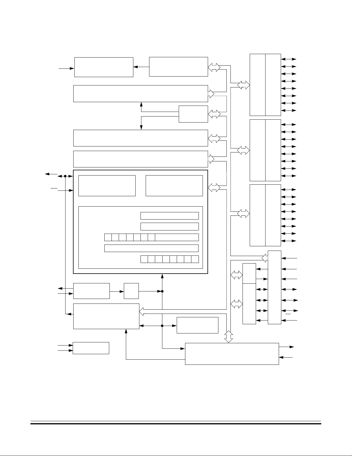
Figure 1-2 shows the structure of the MC68HC705C8A.
Technical Data MC68HC705C8A — Rev. 2.0
22 General Description MOTOROLA
Page 23
General Description
Block Diagram
V
RESET
IRQ
EPROM PROGRAMMING
PP
CONTROL
EPROM/OTPROM — 7744 BYTES
(144 BYTES CONFIGURABLE)
RAM — 176 BYTES
(304 BYTES MAXIMUM)
BOOT ROM — 240 BYTES
CPU
CONTROL
M68HC05 CPU
CPU REGISTERS
PROGRAM COUNTER
CONDITION CODE REGISTER
PROGRAM REGISTER
ARITHMETIC
LOGIC UNIT
ACCUMULATOR
INDEX REGISTER
1100000
STACK POINTER
PORT A
DATA DIRECTION A
OPTION
REGISTER
PORT B
DATA DIRECTION B
PORT C
DATA DIRECTION C
CZNIH111
SCI
PA0
PA1
PA2
PA3
PA4
PA5
PA6
PA7
PB0*
PB1*
PB2*
PB3*
PB4*
PB5*
PB6*
PB7*
PC0
PC1
PC2
PC3
PC4
PC5
PC6
PC7†
PD7
RDI (PD0)
TDO (PD1)
OSC2
OSC1
V
V
OSCILLATOR
COP WATCHDOG
AND
CLOCK MONITOR
DD
SS
POWER
÷ 2
INTERNAL
PROCESSOR
CLOCK
GENERATOR
BAUD RATE
16-BIT
CAPTURE/COMPARE
TIMER SYSTEM
SPI
PORT D
MISO (PD2)
MOSI (PD3)
SCK (PD4)
SS (PD5)
TCMP
TCAP
* Port B pins also function as external interrupts.
† PC7 has a high current sink and source capability.
Figure 1-2. MC68HC705C8A Block Diagram
MC68HC705C8A — Rev. 2.0 TechnicalData
MOTOROLA General Description 23
Page 24

General Description
1.6 Pin Assignments
The MC68HC705C8A is available in six packages:
• 40-pin plastic dual in-line package (PDIP)
• 40-pin ceramic dual in-line package (cerdip)
• 44-lead plastic-leaded chip carrier (PLCC)
• 44-lead ceramic-leaded chip carrier (CLCC)
• 44-pin quad flat pack (QFP)
• 42-pin shrink dual in-line package (SDIP)
The pin assignments for these packages are shown in Figure 1-3,
Figure 1-4, Figure 1-5, and Figure 1-6.
RESET
IRQ
V
PP
PA7
PA6
PA5
PA4
PA3
PA2
PA1
PA0
PB0
PB1
PB2
PB3
PB4
PB5
PB6
PB7
V
1
2
3
4
5
6
7
8
9
10
11
12
13
14
15
16
17
18
19
20
SS
40 V
DD
OSC1
39
OSC2
38
TCAP
37
PD7
36
TCMP
35
PD5/
34
PD4/SCK
33
32
PD3/MOSI
31
PD2/MISO
PD1/TDO
30
29
PD0/RDI
PC0
28
PC1
27
26 PC2
PC3
25
PC4
24
PC5
23
PC6
22
PC7
21
SS
Figure 1-3. 40-Pin PDIP/Cerdip Pin Assignments
Technical Data MC68HC705C8A — Rev. 2.0
24 General Description MOTOROLA
Page 25
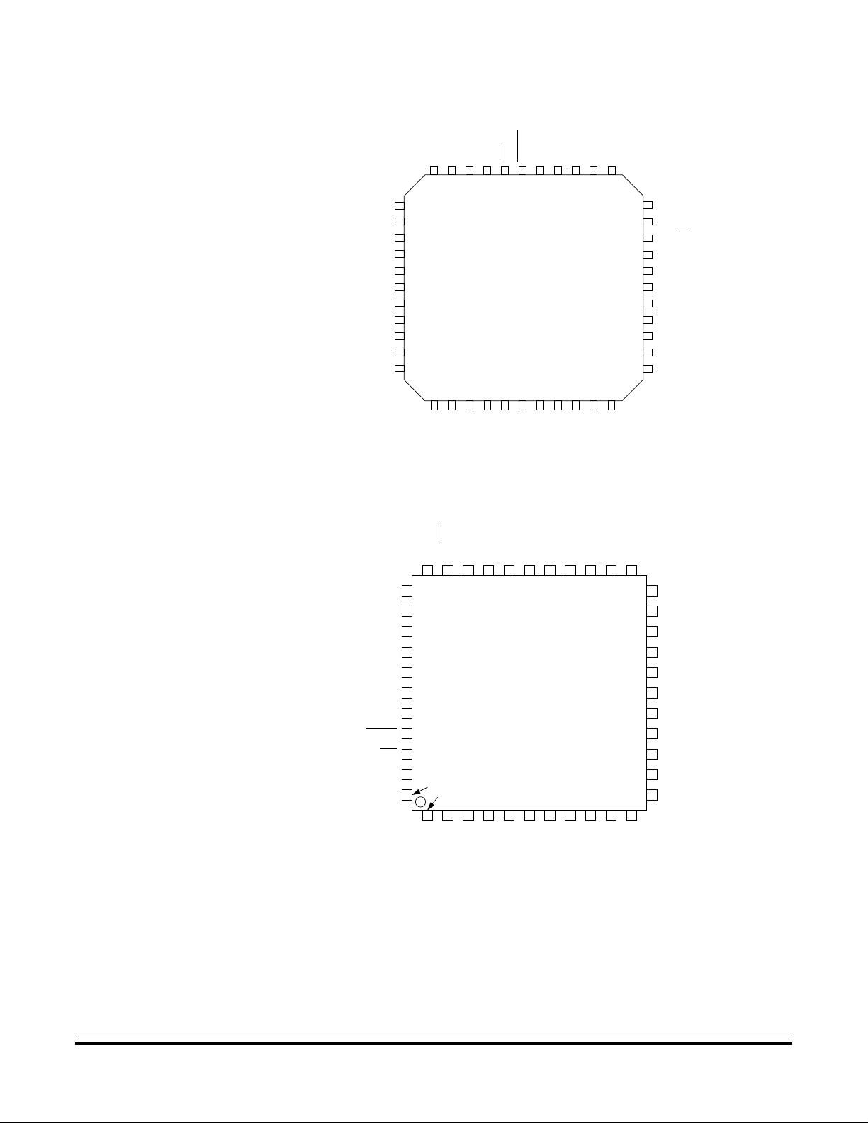
PA5 7
PA4 8
PA3
PA2
PA1
PA0
PB0
PB1
PB2
PB3
PB4
General Description
Pin Assignments
PA6
PA7
VPPNC
IRQ
RESET
VDDOSC1
OSC2
TCAP
NC
6
5
4
3
1
2
4443424140
39
PD7
38
TCMP
9
10
11
12
13
14
15
16
17
26
25
24
23
22
21
20
19
18
37
36
35
34
33
32
31
30
29
28
27
SS
PD5/
PD4/SCK
PD3/MOSI
PD2/MISO
PD1/TDO
PD0/RDI
PC0
PC1
PC2
PB6
PB7
SS
NC
V
PC7
PC6
PC5
PC4
PC3
NC
PB5
Figure 1-4. 44-Lead PLCC/CLCC Pin Assignments
PD3/MOSI
PD2/MISO
PD4/SCK
PD5/SS
PD7
TCAP
OSC2
OSC1
V
DD
NC
NC
RESET
IRQ
V
PP
PA7
TCMP
34
35
36
37
38
39
40
41
42
43
44
234567891011
PD1/TDO
PD0/RDI
PC0
PC1
PC2
PC3
2324252627282930313233
NC
22
PC4
21
PC5
20
PC6
19
PC7
18
V
17
SS
NC
16
PB7
15
PB6
14
PB5
13
PB41
12
PA6
PA5
PA4
PA3
PA2
PA1
PA0
PB0
PB1
PB2
PB3
Figure 1-5. 44-Pin QFP Pin Assignments
MC68HC705C8A — Rev. 2.0 TechnicalData
MOTOROLA General Description 25
Page 26
General Description
RESET
IRQ
V
PP
PA7
PA6
PA5
PA4
PA3
PA2
PA1
PA0
PB0
PB1
PB2
PB3
NC
PB4
PB5
PB6
PB7
V
SS
1
2
3
4
5
6
7
8
9
10
11
12
13
14
15
16
17
18
19
20
21
V
42
DD
OSC1
41
OSC2
40
TCAP
39
PD7
38
TCMP
37
PD5/SS
36
PD4/SCK
35
PD3/MOSI
34
PD2/MISO
33
PD1/TDO
32
PD0/RDI
31
PC0
30
PC1
29
PC2
28
NC
27
PC3
26
25
PC4
PC5
24
23
PC6
22 PC7
Figure 1-6. 42-Pin SDIP Pin Assignments
Technical Data MC68HC705C8A — Rev. 2.0
26 General Description MOTOROLA
Page 27
1.7 Pin Functions
General Description
Pin Functions
This subsection describes the MC68HC705C8A signals. Reference is
made, where applicable, to other sections that contain moredetail about
the function being performed.
1.7.1 V
and V
DD
SS
1.7.2 OSC1 and OSC2
VDDand VSSare the power supply and ground pins. The MCU operates
from a single power supply.
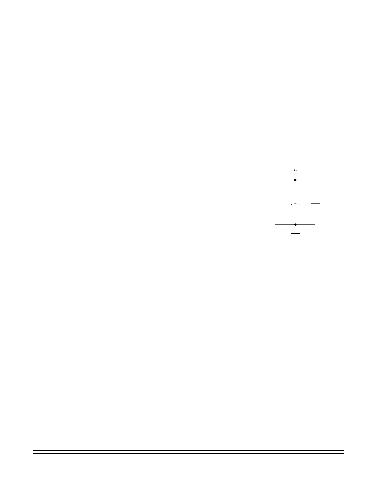
Very fast signal transitions occur
on the MCU pins, placing high
V+
V
DD
short-duration current demands
on the power supply. To prevent
noise problems, take special care
MCU
C1
+
C2
to provide good power supply
V
bypassing at the MCU. Place
SS
bypass capacitors as close to the
MCU as possible, as shown in
Figure 1-7.
Figure 1-7. Bypassing Layout
Recommendation
The OSC1 and OSC2 pins are the control connections for the 2-pin
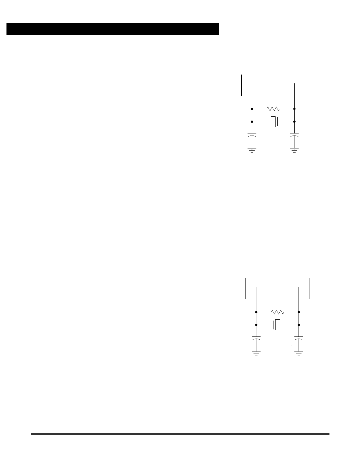
on-chip oscillator. The oscillator can be driven by:
• Crystal resonator
• Ceramic resonator
• External clock signal
NOTE: The frequency of the internal oscillator is f
. The MCU divides the
OSC
internal oscillator output by two to produce the internal clock with a
frequency of f
MC68HC705C8A — Rev. 2.0 Technical Data
MOTOROLA General Description 27
OP
.
Page 28
General Description
1.7.2.1 Crystal Resonator
The circuit in Figure 1-8 shows a
MCU
crystal oscillator circuit for an AT-cut,
parallel resonant crystal. Follow the
crystal supplier’s recommendations,
OSC1
10 MΩ
∗
OSC2
because the crystal parameters
determine the external component
values required to provide reliable
startup and maximum stability. The
22 pF
∗
XTAL
2 MHz
22 pF
∗
load capacitance values used in the
oscillator circuit design should
account for all stray layout
capacitances. To minimize output
distortion, mount the crystal and
capacitorsasclose as possible tothe
∗
Starting value only. Follow crystal supplier’s
recommendations regarding component
values that will provide reliable startup and
maximum stability.
Figure 1-8. Crystal
Connections
pins.
NOTE: Use an AT-cut crystal and not a strip or tuning fork crystal. The MCU
mightoverdrive or havethe incorrect characteristicimpedance for astrip
or tuning fork crystal.
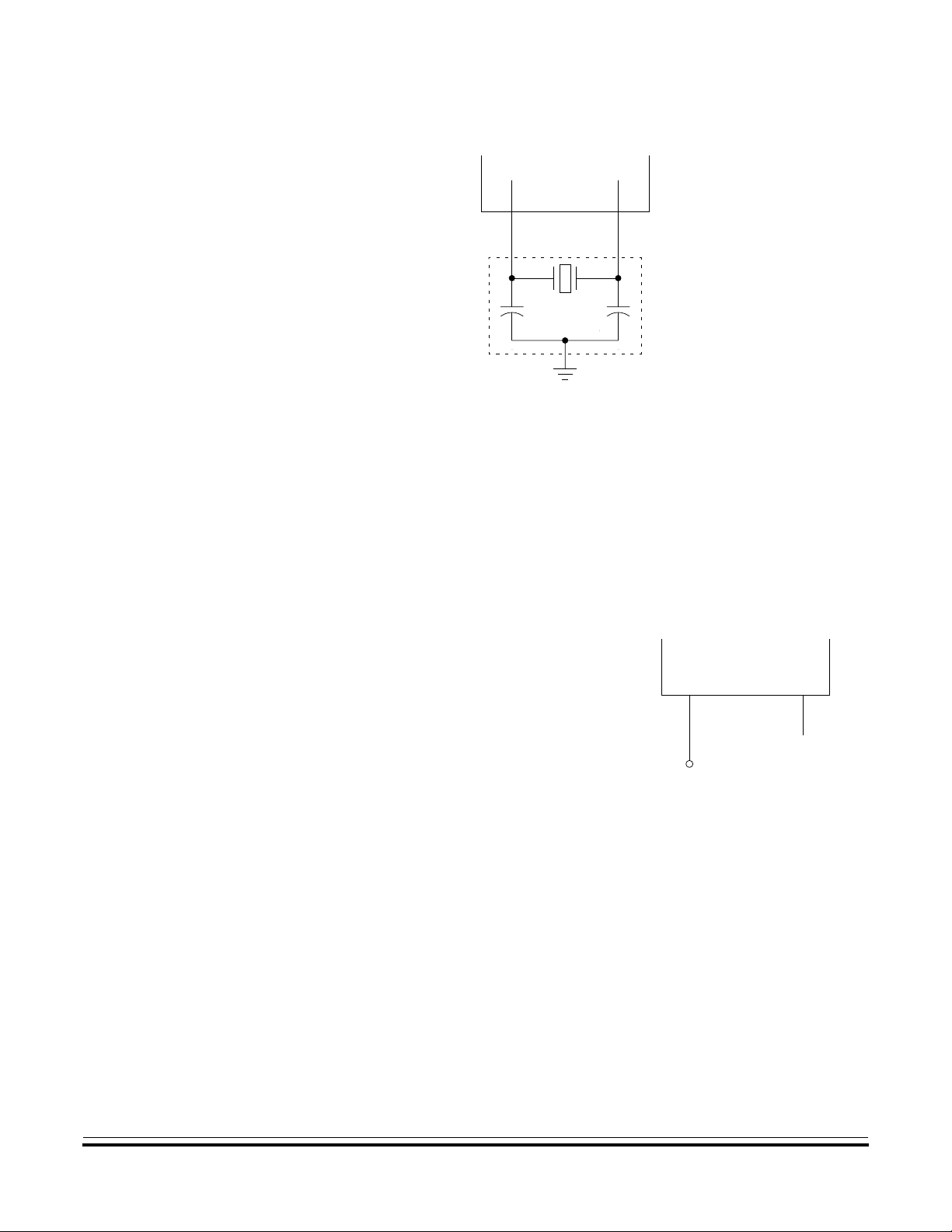
1.7.2.2 Ceramic Resonator
To reduce cost, use a ceramic
MCU
resonator instead of a crystal. Use the
circuit shown in Figure 1-9 for a 2-pin
ceramic resonator or the circuit shown
OSC1
R
OSC2
in Figure 1-10 for a 3-pin ceramic
resonator, and follow the resonator
manufacturer’s recommendations.
CC
CERAMIC
RESONATOR
The external component values
required for maximum stability and
reliable starting depend upon the
resonator parameters. The load
Figure 1-9. 2-Pin Ceramic
Resonator Connections
.
capacitancevalues used in the oscillator circuit designshould include all
stray layout capacitances. To minimize output distortion, mount the
resonator and capacitors as close as possible to the pins.
Technical Data MC68HC705C8A — Rev. 2.0
28 General Description MOTOROLA
Page 29
MCU
OSC1 OSC2
CERAMIC
RESONATOR
Figure 1-10. 3-Pin
Ceramic Resonator
Connections
General Description
Pin Functions
NOTE: The bus frequency (f
(f
OSC
period.
1.7.2.3 External Clock Signal
An external clock from another
CMOS-compatible device can drive the
OSC1 input, with the OSC2 pin
unconnected, as Figure 1-11 shows.
NOTE: The bus frequency (f
the processor clock cycle is two times the f
) is one-half the external or crystal frequency
OP
), while the processor clock cycle (t
) is one-half the external frequency (f
OP
) is two times the f
CYC
MCU
OSC1
EXTERNAL
CMOS CLOCK
Figure 1-11. External
Clock
period.
OSC
OSC
OSC
OSC2
) while
MC68HC705C8A — Rev. 2.0 Technical Data
MOTOROLA General Description 29
Page 30

General Description
1.7.3 External Reset Pin (RESET)
A logic 0 on the bidirectional
startup state. The
RESET pin contains an internal Schmitt trigger as part
of its input to improve noise immunity. See Section 5. Resets.
1.7.4 External Interrupt Request Pin (IRQ)
IRQ pin is an asynchronous external interrupt pin. The IRQ pin
The
contains an internal Schmitt trigger as part of its input to improve noise
immunity. See 4.3.2 External Interrupt (IRQ).
1.7.5 Input Capture Pin (TCAP)
The TCAP pin is the input capture pin for the on-chip capture/compare
timer. The TCAP pin contains an internal Schmitt trigger as part of its
input to improve noise immunity. See Section 8. Capture/Compare
Timer.
RESET pin forces the MCU to a known
1.7.6 Output Compare Pin (TCMP)
The TCMP pin is the output compare pin for the on-chip
capture/compare timer. See Section 8. Capture/Compare Timer.
1.7.7 Port A I/O Pins (PA7–PA0)
These eight I/O lines comprise port A, a general-purpose, bidirectional
I/O port. The pins are programmable as either inputs or outputs under
software control of the data direction registers. See 7.3 Port A.
1.7.8 Port B I/O Pins (PB7–PB0)
These eight I/O pins comprise port B, a general-purpose, bidirectional
I/O port. The pins are programmable as either inputs or outputs under
software control of the data direction registers. Port B pins also can be
configured to function as external interrupts. See 7.4 Port B.
Technical Data MC68HC705C8A — Rev. 2.0
30 General Description MOTOROLA
Page 31

1.7.9 Port C I/O Pins (PC7–PC0)
These eight I/O pins comprise port C, a general-purpose, bidirectional
I/O port. The pins are programmable as either inputs or outputs under
software control of the data direction registers. PC7 has a high current
sink and source capability. See 7.5 Port C.
1.7.10 Port D I/O Pins (PD7 and PD5–PD0)
These seven lines comprise port D, a fixed input port. All special
functions that are enabled (SPI and SCI) affect this port. See 7.6 Port D.
General Description
Pin Functions
NOTE: Connecting the V
result in damage to the MCU.
pin (programming voltage) to VSS (ground) could
PP
MC68HC705C8A — Rev. 2.0 Technical Data
MOTOROLA General Description 31
Page 32

General Description
Technical Data MC68HC705C8A — Rev. 2.0
32 General Description MOTOROLA
Page 33

Technical Data — MC68HC705C8A
2.1 Contents
2.2 Introduction. . . . . . . . . . . . . . . . . . . . . . . . . . . . . . . . . . . . . . . .33
2.3 Memory Map. . . . . . . . . . . . . . . . . . . . . . . . . . . . . . . . . . . . . . .33
2.4 Input/Output (I/O) . . . . . . . . . . . . . . . . . . . . . . . . . . . . . . . . . . .34
2.5 RAM . . . . . . . . . . . . . . . . . . . . . . . . . . . . . . . . . . . . . . . . . . . . .34
2.6 EPROM/OTPROM (PROM) . . . . . . . . . . . . . . . . . . . . . . . . . . .35
2.7 Bootloader ROM. . . . . . . . . . . . . . . . . . . . . . . . . . . . . . . . . . . .35
Section 2. Memory
2.2 Introduction
2.3 Memory Map
This section describes the organization of the on-chip memory.
The central processor unit (CPU) can address eight Kbytes of memory
andinput/output (I/O) registers. The program counter typically advances
oneaddress at a timethrough memory, reading theprogram instructions
and data. The programmable read-only memory (PROM) portion of
memory — either one-time programmable read-only memory
(OTPROM) or erasable, programmable read-only memory
(EPROM) — holds the program instructions, fixed data, user-defined
vectors, and interrupt service routines. The random-access memory
(RAM) portion of memory holds variable data.
I/O registers are memory-mapped so that the CPU can access their
locations in the same way that it accesses all other memory locations.
The shared stack area is used during processing of an interrupt or
MC68HC705C8A — Rev. 2.0 Technical Data
MOTOROLA Memory 33
Page 34

Memory
2.4 Input/Output (I/O)
subroutine call to save the CPU state. The stack pointer decrements
during pushes and increments during pulls.
Figure 2-1 is a memory map of the MCU. Addresses $0000–$001F,
shown in Figure 2-2, contain most of the control, status, and data
registers. Additional I/O registers have these addresses:
• $1FDF, option register
• $1FF0, mask option register 1 (MOR1)
• $1FF1, mask option register 2 (MOR2)
The first 32 addresses of memory space, from $0000 to $001F, are the
I/O section. These are the addresses of the I/O control registers, status
registers, and data registers. See Figure 2-2 for more information.
2.5 RAM
One of four selectable memory configurations is selected by the state of
the RAM1 and RAM0 bits in the option register located at $1FDF. Reset
or power-on reset (POR) clears these bits, automatically selecting the
first memory configuration as shown in Table 2-1. See 9.5.1 Option
Register.
Table 2-1. Memory Configurations
RAM0 RAM1 RAM Bytes PROM Bytes
0 0 176 7744
1 0 208 7696
0 1 272 7648
1 1 304 7600
NOTE: Be careful when using nested subroutines or multiple interrupt levels.
The CPU can overwrite data in the stack RAM during a subroutine or
during the interrupt stacking operation.
Technical Data MC68HC705C8A — Rev. 2.0
34 Memory MOTOROLA
Page 35

2.6 EPROM/OTPROM (PROM)
AnMCU with a quartzwindow has a maximumof 7744 bytesofEPROM.
The quartz window allows the EPROM erasure with ultraviolet light. In
an MCU without a quartz window, the EPROM cannot be erased and
serves a maximum 7744 bytes of OTPROM (see Table 2-1). See
Section 9. EPROM/OTPROM (PROM).
2.7 Bootloader ROM
The 240 bytes at addresses $1F00–$1FEF are reserved ROM
addresses that contain the instructions for the bootloader functions. See
Section 9. EPROM/OTPROM (PROM).
Memory
EPROM/OTPROM (PROM)
MC68HC705C8A — Rev. 2.0 Technical Data
MOTOROLA Memory 35
Page 36

Memory
$0000
$001F PORT C DATA REGISTER $0002
$0020
$002F PORT B DATA DIRECTION REGISTER $0005
$0030
$004F RAM0 = 1
$0050 SPI CONTROL REGISTER $000A
$00BF SPI DATA REGISTER $000C
$00C0
$00FF SCI CONTROL REGISTER 2 $000F
$0100
USER PROM
$015F RAM1 = 0
$0160
$1EFF ALTERNATE TIMER REGISTER (LOW) $001B
$1F00
$1FDE COP CONTROL REGISTER $001E
$1FDF OPTION REGISTER UNUSED $001F
$1FE0
$1FEF
$1FF0 MASK OPTION REGISTER 1
$1FF1 MASK OPTION REGISTER 2
$1FF2
$1FFF TIMER INTERRUPT VECTOR (HIGH) $1FF8
(1)
See 9.5.1 Option Register for information. EXTERNAL INTERRUPT VECTOR (LOW) $1FFB
I/O REGISTERS
32 BYTES
UNUSED
16 BYTES
RAM
32 BYTES
(1)
RAM
176 BYTES
96 BYTES
(1)
USER PROM
7584 BYTES
BOOTLOADER ROM
240 BYTES
BOOT ROM VECTORS
16 BYTES
USER PROM VECTORS
12 BYTES
USER PROM
48 BYTES
(1)
RAM0 = 0
STACK
64 BYTES
RAM
96 BYTES
(1)
RAM1 = 1
PORT A DATA REGISTER $0000
PORT B DATA REGISTER $0001
PORT D FIXED INPUT PORT $0003
PORT A DATA DIRECTION REGISTER $0004
PORT C DATA DIRECTION REGISTER $0006
UNUSED $0007
UNUSED $0008
UNUSED $0009
SPI STATUS REGISTER $000B
SCI BAUD RATE REGISTER $000D
SCI CONTROL REGISTER 1 $000E
SCI STATUS REGISTER $0010
SCI DATA REGISTER $0011
TIMER CONTROL REGISTER $0012
TIMER STATUS REGISTER $0013
INPUT CAPTURE REGISTER (HIGH) $0014
INPUT CAPTURE REGISTER (LOW) $0015
OUTPUT COMPARE REGISTER (HIGH) $0016
OUTPUT COMPARE REGISTER (LOW) $0017
TIMER REGISTER (HIGH) $0018
TIMER REGISTER (LOW) $0019
ALTERNATE TIMER REGISTER (HIGH) $001A
EPROM PROGRAM REGISTER $001C
COP RESET REGISTER $001D
RESERVED $1FF2
RESERVED $1FF3
SPI INTERRUPT VECTOR (HIGH) $1FF4
SPI INTERRUPT VECTOR (LOW) $1FF5
SCI INTERRUPT VECTOR (HIGH) $1FF6
SCI INTERRUPT VECTOR (LOW) $1FF7
TIMER INTERRUPT VECTOR (LOW) $1FF9
EXTERNAL INTERRUPT VECTOR (HIGH) $1FFA
SOFTWARE INTERRUPT VECTOR (HIGH) $1FFC
SOFTWARE INTERRUPT VECTOR (LOW) $1FFD
RESET VECTOR (HIGH) $1FFE
RESET VECTOR (LOW) $1FFF
Figure 2-1. Memory Map
Technical Data MC68HC705C8A — Rev. 2.0
36 Memory MOTOROLA
Page 37

Memory
Bootloader ROM
Addr. Register Name Bit 7 6 5 4 3 2 1 Bit 0
$0000
$0001
$0002
$0003
$0004
Port A Data Register
(PORTA)
See page 76.
Port B Data Register
(PORTB)
See page 79.
Port C Data Register
(PORTC)
See page 83.
Port D Fixed Input Register
(PORTD)
See page 86.
Port A Data Direction
Register (DDRA)
See page 77.
Read:
PA7 PA6 PA5 PA4 PA3 PA2 PA1 PA0
Write:
Reset: Unaffected by reset
Read:
PB7 PB6 PB5 PB4 PB3 PB2 PB1 PB0
Write:
Reset: Unaffected by reset
Read:
PC7 PC6 PC5 PC4 PC3 PC2 PC1 PC0
Write:
Reset: Unaffected by reset
Read: PD7
Write:
Reset: Unaffected by reset
Read:
DDRA7 DDRA6 DDRA5 DDRA4 DDRA3 DDRA2 DDRA1 DDRA0
Write:
Reset: 0 0 0 0 0 0 0 0
SS SCK MOSI MISO TDO RDI
Port B Data Direction
$0005
$0006
$0007 Unimplemented
$0008 Unimplemented
$0009 Unimplemented
Register (DDRB)
See page 80.
Port C Data Direction
(DDRC)
See page 84.
Figure 2-2. I/O Register Summary (Sheet 1 of 4)
Read:
DDRB7 DDRB6 DDRB5 DDRB4 DDRB3 DDRB2 DDRB1 DDRB0
Write:
Reset: 0 0 0 0 0 0 0 0
Read:
DDRC7 DDRC6 DDRC5 DDRC4 DDRC3 DDRC2 DDRC1 DDRC0
Write:
Reset: 0 0 0 0 0 0 0 0
= Unimplemented U = Unaffected
MC68HC705C8A — Rev. 2.0 Technical Data
MOTOROLA Memory 37
Page 38

Memory
Addr. Register Name Bit 7 6 5 4 3 2 1 Bit 0
$000A
$000B
$000C
$000D
$000E
SPI Control Register
(SPCR)
See page 147.
SPI Status Register
(SPSR)
See page 149.
SPI Data Register
(SPDR)
See page 147.
Baud Rate Register
(Baud)
See page 134.
SCI Control Register 1
(SCCR1)
See page 128.
Read:
SPIE SPE
Write:
Reset: 0 0 0 U U U U
Read: SPIF WCOL MODF
Write:
Reset: 0 0 0
Read:
Bit 7 Bit 6 Bit 5 Bit 4 Bit 3 BIt 2 Bit 1 Bit 0
Write:
Reset: Unaffected by reset
Read:
SCP1 SCP0 SCR2 SCR1 SCR0
Write:
Reset: U U 0 0 U U U U
Read:
R8 T8 M WAKE
Write:
Reset: U U U U
MSTR CPOL CPHA SPR1 SPR0
$000F
$0010
$0011
$0012
SCI Control Register 2
(SCCR2)
See page 129.
SCI Status Register
(SCSR)
See page 131.
SCI Data Register
(SCDR)
See page 127.
Timer Control Register
(TCR)
See page 92.
Figure 2-2. I/O Register Summary (Sheet 2 of 4)
Read:
TIE TCIE RIE ILIE TE RE RWU SBK
Write:
Reset: 0 0 0 0 0 0 0 0
Read: TDRE TC RDRF IDLE OR NF FE
Write:
Reset: 1 1 0 0 0 0 0 U
Read:
Bit 7 Bit 6 Bit 5 Bit 4 Bit 3 Bit 2 Bit 1 Bit 0
Write:
Reset: Unaffected by reset
Read:
ICIE OCIE TOIE 0 0 0 IEDG OLVL
Write:
Reset: 0 0 0 0 0 0 U 0
= Unimplemented U = Unaffected
Technical Data MC68HC705C8A — Rev. 2.0
38 Memory MOTOROLA
Page 39

Memory
Bootloader ROM
Addr. Register Name Bit 7 6 5 4 3 2 1 Bit 0
$0013
$0014
$0015
$0016
$0017
Timer Status Register
(TSR)
See page 94.
Input Capture Register
High (ICRH)
See page 98.
Input Capture Register
Low (ICRL)
See page 98.
Output Compare Register
High (OCRH)
See page 99.
Output Compare Register
Low (OCRL)
See page 99.
Read: ICF OCF TOF 0 0 0 0 0
Write:
Reset: U U U 0 0 0 0 0
Read: Bit 15 Bit 14 Bit 13 Bit 12 Bit 11 Bit 10 Bit 9 Bit 8
Write:
Reset: Unaffected by reset
Read: Bit 7 Bit 6 Bit 5 Bit 4 Bit 3 Bit 2 Bit 1 Bit 0
Write:
Reset: Unaffected by reset
Read:
Bit 15 Bit 14 Bit 13 Bit 12 Bit 11 Bit 10 Bit 9 Bit 8
Write:
Reset: Unaffected by reset
Read:
Bit 7 Bit 6 Bit 5 Bit 4 Bit 3 Bit 2 Bit 1 Bit 0
Write:
Reset: Unaffected by reset
$0018
$0019
$001A
$001B
Timer Register High
(TRH)
See page 95.
Timer Register Low
(TRL)
See page 95.
Alternate Timer Register
High (ATRH)
See page 97.
Alternate Timer Register
Low (ATRL)
See page 97.
Figure 2-2. I/O Register Summary (Sheet 3 of 4)
Read: Bit 15 Bit 14 Bit 13 Bit 12 Bit 11 Bit 10 Bit 9 Bit 8
Write:
Reset: Reset initializes TRH to $FF
Read: Bit 7 Bit 6 Bit 5 Bit 4 Bit 3 Bit 2 Bit 1 Bit 0
Write:
Reset: Reset initializes TRL to $FC
Read: Bit 15 Bit 14 Bit 13 Bit 12 Bit 11 Bit 10 Bit 9 Bit 8
Write:
Reset: Reset initializes ATRH to $FF
Read: Bit 7 Bit 6 Bit 5 Bit 4 Bit 3 Bit 2 Bit 1 Bit 0
Write:
Reset: Reset initializes ATRL to $FC
= Unimplemented U = Unaffected
MC68HC705C8A — Rev. 2.0 Technical Data
MOTOROLA Memory 39
Page 40

Memory
Addr. Register Name Bit 7 6 5 4 3 2 1 Bit 0
EPROM Programming
$001C
Programmable COP Reset
$001D
Programmable COP Control
$001E
$001F Unimplemented
$1FDF
Register (PROG)
See page 107.
Register (COPRST)
See page 62.
Register (COPCR)
See page 62.
Option Register
(Option)
See page 114.
Read:
0 0 0 0 0 LAT 0 PGM
Write:
Reset: 0 0 0 0 0 0 0 0
Read:
Write: Bit 7 Bit 6 Bit 5 Bit 4 Bit 3 Bit 2 Bit 1 Bit 0
Reset: U U U U U U U U
Read: 0 0 0 COPF
CME PCOPE CM1 CM0
Write:
Reset: 0 0 0 U 0 0 0 0
Read:
RAM0 RAM1 0 0 SEC* IRQ 0
Write:
Reset: 0 0 0 0 * U10
*Implemented as an EPROM cell
$1FF0
$1FF1
Mask Option Register 1
(MOR1)
See page 115.
Mask Option Register 2
(MOR2)
See page 116.
Read:
PBPU7 PBPU6 PBPU5 PBPU4 PBPU3 PBPU2 PBPU1
Write:
Reset: Unaffected by reset
Read:
Write:
Reset: Unaffected by reset
= Unimplemented U = Unaffected
PBPU0/
COPC
NCOPE
Figure 2-2. I/O Register Summary (Sheet 4 of 4)
Technical Data MC68HC705C8A — Rev. 2.0
40 Memory MOTOROLA
Page 41

Technical Data — MC68HC705C8A
Section 3. Central Processor Unit (CPU)
3.1 Contents
3.2 Introduction. . . . . . . . . . . . . . . . . . . . . . . . . . . . . . . . . . . . . . . .41
3.3 CPU Registers . . . . . . . . . . . . . . . . . . . . . . . . . . . . . . . . . . . . .42
3.3.1 Accumulator . . . . . . . . . . . . . . . . . . . . . . . . . . . . . . . . . . . .43
3.3.2 Index Register . . . . . . . . . . . . . . . . . . . . . . . . . . . . . . . . . . .43
3.3.3 Stack Pointer . . . . . . . . . . . . . . . . . . . . . . . . . . . . . . . . . . . .44
3.3.4 Program Counter . . . . . . . . . . . . . . . . . . . . . . . . . . . . . . . . .44
3.3.5 Condition Code Register . . . . . . . . . . . . . . . . . . . . . . . . . . .45
3.4 Arithmetic/Logic Unit (ALU) . . . . . . . . . . . . . . . . . . . . . . . . . . .46
3.2 Introduction
This section describes the central processor unit (CPU) registers.
MC68HC705C8A — Rev. 2.0 Technical Data
MOTOROLA Central Processor Unit (CPU) 41
Page 42

Central Processor Unit (CPU)
3.3 CPU Registers
Figure 3-1 shows the fiveCPU registers. These arehard-wired registers
within the CPU and are not part of the memory map.
Bit 04Bit 7 56 321
ACCUMULATOR (A)
Bit 04Bit 7 56 321
INDEX REGISTER (X)
8Bit 12 11 10 9
110000 0
8Bit 12 11 10 9
6 321
HALF-CARRY FLAG
INTERRUPT MASK
NEGATIVE FLAG
ZERO FLAG
CARRY/BORROW FLAG
Figure 3-1. Programming Model
Bit 04756 321
STACK POINTER (SP)
Bit 04756 321
PROGRAM COUNTER (PC)
Bit 04Bit 7 5
ZCIN1H11
CONDITION CODE REGISTER (CCR)
Technical Data MC68HC705C8A — Rev. 2.0
42 Central Processor Unit (CPU) MOTOROLA
Page 43

3.3.1 Accumulator
3.3.2 Index Register
Central Processor Unit (CPU)
CPU Registers
The accumulator (A) shown in Figure 3-2 is a general-purpose 8-bit
register. The CPU uses the accumulator to hold operands and results of
arithmetic and non-arithmetic operations.
Bit 7 654321Bit 0
Read:
Write:
Reset: Unaffected by reset
Figure 3-2. Accumulator (A)
In the indexed addressing modes, the CPU uses the byte in the index
register (X) shown in Figure 3-3 to determine the conditional address of
the operand. See 12.3.5 Indexed, No Offset, 12.3.6 Indexed, 8-Bit
Offset, and 12.3.7 Indexed, 16-Bit Offset for more information on
indexed addressing.
The 8-bit index register also can serve as a temporary data storage
location.
Bit 7 654321Bit 0
Read:
Write:
Reset: Unaffected by reset
Figure 3-3. Index Register (X)
MC68HC705C8A — Rev. 2.0 Technical Data
MOTOROLA Central Processor Unit (CPU) 43
Page 44

Central Processor Unit (CPU)
3.3.3 Stack Pointer
The stack pointer (SP) shown in Figure 3-4 is a 13-bit register that
contains the address of the next free location on the stack. During a
reset or after the reset stack pointer (RSP) instruction, the stack pointer
initializesto$00FF. The address inthestack pointer decrements asdata
is pushed onto the stack and increments as data is pulled from the stack.
The seven most significant bits of the stack pointer are fixed
permanently at 0000011, so the stack pointer produces addresses from
$00C0 to $00FF. If subroutines and interrupts use more than 64 stack
locations, the stack pointer wraps around to address $00FF and begins
writing over the previously stored data. A subroutine uses two stack
locations. An interrupt uses five locations.
Bit 12 11 10 9 87654321Bit 0
Read: 0 0 0 0 0 1 1
Write:
Reset: 0 0 0 0 011111111
3.3.4 Program Counter
Bit 12 11 10 987654321Bit 0
= Unimplemented
Figure 3-4. Stack Pointer (SP)
The program counter (PC) shown in Figure 3-5 is a 13-bit register that
contains the address of the next instruction or operand to be fetched.
Normally, the address in the program counter automatically increments
to the next sequential memory location every time an instruction or
operand is fetched. Jump, branch, and interrupt operations load the
program counter with an address other than that of the next sequential
location.
Read:
Write:
Reset: Loaded with reset vector from $1FFE and $1FFF
Figure 3-5. Program Counter (PC)
Technical Data MC68HC705C8A — Rev. 2.0
44 Central Processor Unit (CPU) MOTOROLA
Page 45

3.3.5 Condition Code Register
The condition code register (CCR) shown in Figure 3-6 is an 8-bit
register whose three most significant bits are permanently fixed at 111.
Thecondition code registercontains the interrupt mask and four bits that
indicate the results of prior instructions.
Read: 1 1 1
Write:
Reset: 1 1 1 U 1 U U U
Central Processor Unit (CPU)
CPU Registers
Bit 7 654321Bit 0
HINZC
= Unimplemented U = Unaffected
Figure 3-6. Condition Code Register (CCR)
H — Half-Carry Bit
The CPU sets the half-carry flag when a carry occurs between bits 3
and 4 of the accumulator during an add without carry (ADD) or add
with carry (ADC) operation. The half-carry bit is required for
binary-coded decimal (BCD) arithmetic operations. Reset has no
affect on the half-carry flag.
I — Interrupt Mask Bit
Setting the interrupt mask (I) disables interrupts. If an interrupt
request occurs while the interrupt mask is a logic 0, the CPU saves
the CPU registers on the stack, sets the interrupt mask, and then
fetches the interrupt vector. If an interrupt request occurs while the
interrupt mask is set, the interrupt request is latched. The CPU
processes the latched interrupt as soon as the interrupt mask is
cleared again.
A return-from-interrupt (RTI) instruction pulls the CPU registers from
the stack, restoring the interrupt mask to its cleared state. After a
reset, the interrupt mask is set and can be cleared only by a CLI,
STOP, or WAIT instruction.
MC68HC705C8A — Rev. 2.0 Technical Data
MOTOROLA Central Processor Unit (CPU) 45
Page 46

Central Processor Unit (CPU)
N — Negative Flag
The CPU sets the negative flag when an arithmetic operation, logical
operation,ordata manipulation produces a negativeresult(bit7 in the
results is a logic 1). Reset has no effect on the negative flag.
Z — Zero Flag
The CPU sets the zero flag when an arithmetic operation, logical
operation, or data manipulation produces a result of $00. Reset has
no effect on the zero flag.
C — Carry/Borrow Flag
The CPU sets the carry/borrow flag when an addition operation
produces a carry out of bit 7 of the accumulator or when a subtraction
operation requires a borrow. Some logical operations and data
manipulation instructions also clear or set the carry/borrow bit. Reset
has no effect on the carry/borrow flag.
3.4 Arithmetic/Logic Unit (ALU)
The arithmetic/logic unit (ALU) performs the arithmetic and logical
operations defined by the instruction set. The binary arithmetic circuits
decode instructions and set up the ALU for the selected operation. Most
binary arithmetic is based on the addition algorithm, carrying out
subtraction as negative addition. Multiplication is not performed as a
discrete operation but as a chain of addition and shift operations within
the ALU. The multiply instruction requires 11 internal clock cycles to
complete this chain of operations.
Technical Data MC68HC705C8A — Rev. 2.0
46 Central Processor Unit (CPU) MOTOROLA
Page 47

Technical Data — MC68HC705C8A
4.1 Contents
4.2 Introduction. . . . . . . . . . . . . . . . . . . . . . . . . . . . . . . . . . . . . . . .47
4.3 Interrupt Sources . . . . . . . . . . . . . . . . . . . . . . . . . . . . . . . . . . .48
4.3.1 Software Interrupt. . . . . . . . . . . . . . . . . . . . . . . . . . . . . . . . .48
4.3.2 External Interrupt (
4.3.3 Port B Interrupts. . . . . . . . . . . . . . . . . . . . . . . . . . . . . . . . . .51
4.3.4 Capture/Compare Timer Interrupts . . . . . . . . . . . . . . . . . . .53
4.3.5 SCI Interrupts. . . . . . . . . . . . . . . . . . . . . . . . . . . . . . . . . . . .53
4.3.6 SPI Interrupts . . . . . . . . . . . . . . . . . . . . . . . . . . . . . . . . . . . .54
4.4 Interrupt Processing . . . . . . . . . . . . . . . . . . . . . . . . . . . . . . . . .55
Section 4. Interrupts
IRQ) . . . . . . . . . . . . . . . . . . . . . . . . . . . .49
4.2 Introduction
This section describes how interrupts temporarily change the normal
processing sequence.
MC68HC705C8A — Rev. 2.0 Technical Data
MOTOROLA Interrupts 47
Page 48

Interrupts
4.3 Interrupt Sources
These sources can generate interrupts:
• Software instructions (SWI)
• External interrupt pin (IRQ)
• Port B pins
• Serial communications interface (SCI):
– SCI transmit data register empty
– SCI transmission complete
– SCI receive data register full
– SCI receiver overrun
– SCI receiver input idle
The
setting the I bit of the condition code register (CCR). The software
interrupt (SWI) instruction is non-maskable.
An interrupt temporarily changes the program sequence to process a
particular event. An interrupt does not stop the execution of the
instruction in progress but takes effect when the current instruction
completes its execution. Interrupt processing automatically saves the
central processor unit (CPU) registers on the stack and loads the
program counter with a user-defined vector address.
4.3.1 Software Interrupt
• Serial peripheral interface (SPI):
– SPI transmission complete
– SPI mode fault
– SPI overrun
IRQ pin, port B pins, SCI, and SPI can be masked (disabled) by
The software interrupt instruction (SWI) causes a non-maskable
interrupt.
Technical Data MC68HC705C8A — Rev. 2.0
48 Interrupts MOTOROLA
Page 49

4.3.2 External Interrupt (IRQ)
Interrupts
Interrupt Sources
An interrupt signal on the
IRQ pin latches an external interrupt request.
After completing the current instruction, the CPU tests these bits:
• IRQ latch
• I bit in the CCR
Setting the I bit in the CCR disables external interrupts.
If the IRQ latch is set and the I bit is clear, the CPU then begins the
interrupt sequence. The CPU clears the IRQ latch while it fetches the
interrupt vector,so thatanother external interrupt request can be latched
during the interrupt service routine. As soon as the I bit is cleared during
the return-from-interrupt (RTI) instruction, the CPU can recognize the
newinterrupt request. Figure 4-1 shows the logic forexternal interrupts.
Figure 4-1 shows an external interrupt functional diagram. Figure 4-2
shows an external interrupt timing diagram for the interrupt line. The
timing diagram illustrates two treatments of the interrupt line to the
processor.
1. Two single pulses on the interrupt line are spaced far enough
apart to be serviced. The minimum time between pulses is a
function of the length of the interrupt service.
Once a pulse occurs, the next pulse normally should not occur
until an RTI occurs. This time (t
) is obtained by adding 19
ILIL
instructioncyclestothe total number of cycles neededtocomplete
the service routine (not including the RTI instruction).
2. Many interrupt lines are “wire-ORed” to the
IRQ line. If the
interrupt line remains low after servicing an interrupt, then the
CPU continues to recognize an interrupt.
NOTE: The internal interrupt latch is cleared in the first part of the interrupt
service routine. Therefore, a new external interrupt pulse could be
latched and serviced as soon as the I bit is cleared.
If the
IRQ pin is not in use, connect it to the VDD pin.
MC68HC705C8A — Rev. 2.0 Technical Data
MOTOROLA Interrupts 49
Page 50

Interrupts
EDGE- AND LEVEL-SENSITIVE TRIGGER
OPTION REGISTER
V
DD
DQ
IRQ LATCH
EXTERNAL
INTERRUPT
REQUEST
I BIT (CCR)
INTERRUPT PIN
C
Q
R
Figure 4-1. External Interrupt Internal Function Diagram
t
ILIL
IRQ PIN
a. Edge-Sensitive Trigger Condition. The minimum pulse width (t
or 250 ns (f
= 1 MHz). The period t
OP
execute the interrupt service routine plus 19 t
t
ILIH
should not be less than the number of t
ILIL
CYC
cycles.
POR
INTERNAL RESET (COP)
EXTERNAL RESET
EXTERNAL INTERRUPT BEING SERVICED
(VECTOR FETCH)
) is either 125 ns (fOP = 2.1 MHz)
ILIH
cycles it takes to
CYC
t
ILIH
NORMALLY
USED WITH
WIRED-OR
CONNECTION
IRQ
1
.
.
.
IRQ
n
IRQ
(INTERNAL)
b. Level-Sensitive Trigger Condition. If the interrupt line remains low after servicing an interrupt, then the
CPU continues to recognize an interrupt.
Figure 4-2. External Interrupt Timing
Technical Data MC68HC705C8A — Rev. 2.0
50 Interrupts MOTOROLA
Page 51

4.3.3 Port B Interrupts
Interrupts
Interrupt Sources
When these three conditions are true, a port B pin (PBx) acts as an
external interrupt pin:
• The corresponding port B pullup bit (PBPUx) in mask option
register 1 (MOR1) is programmed to a logic 1.
• The corresponding port B data direction bit (DDRBx) in data
direction register B (DDRB) is a logic 0.
• The clear interrupt mask (CLI) instruction has cleared the I bit in
the CCR.
MOR1 is an erasable, programmable read-only memory (EPROM)
register that enables the port B pullup device. Data from MOR1 is
latched on the rising edge of the voltage on the
RESET pin. See 9.5.2
Mask Option Register 1.
Port B external interrupt pins can be falling-edge sensitive only or both
falling-edge and low-level sensitive, depending on the state of the IRQ
bit in the option register at location $1FDF.
When the IRQ bit is a logic 1, a falling edge or a low level on a port B
external interrupt pin latches an external interrupt request. As long as
any port B external interrupt pin is low, an external interrupt request is
present, and the CPU continues to execute the interrupt service routine.
When the IRQ bit is a logic 0, a falling-edge only on a port B external
interrupt pin latches an external interrupt request. A subsequent port B
external interrupt request can be latched only after the voltage level of
the previous port B external interrupt signal returns to a logic 1 and then
falls again to a logic 0.
Figure 4-3 shows the port B input/output (I/O) logic.
MC68HC705C8A — Rev. 2.0 Technical Data
MOTOROLA Interrupts 51
Page 52

Interrupts
READ $0005
PBPU7
FROM MOR1
V
DD
FROM OTHER
PORT B PINS
IRQ
INTERNAL DATA BUS
WRITE $0005
RESET
WRITE $0001
READ $0001
FROM OPTION
REGISTER
IRQ
DATA DIRECTION
REGISTER B
BIT DDRB7
PORT B DATA
REGISTER
BIT PB7
PB7
V
DD
EXTERNAL
D
Q
C
Q
R
I BIT
FROM CCR
INTERRUPT
REQUEST
RESET
EXTERNAL INTERRUPT VECTOR FETCH
Figure 4-3. Port B I/O Logic
Technical Data MC68HC705C8A — Rev. 2.0
52 Interrupts MOTOROLA
Page 53

4.3.4 Capture/Compare Timer Interrupts
Setting the I bit in the CCR disables all interrupts except for SWI.
4.3.5 SCI Interrupts
The serial communications interface (SCI) can generate these
interrupts:
• Transmit data register empty interrupt
• Transmission complete interrupt
• Receive data register full interrupt
• Receiver overrun interrupt
• Receiver input idle interrupt
Interrupts
Interrupt Sources
Setting the I bit in the CCR disables all SCI interrupts.
• SCI Transmit Data Register Empty Interrupt — The transmit
data register empty bit (TDRE) indicates that the SCI data register
is ready to receive a byte for transmission. TDRE becomes set
when data in the SCI data register transfers to the transmit shift
register. TDRE generates an interrupt request if the transmit
interrupt enable bit (TIE) is set also.
• SCI Transmission Complete Interrupt — The transmission
completebit (TC) indicates thecompletion of an SCItransmission.
TC becomes set when the TDRE bit becomes set and no data,
preamble, or break character is being transmitted. TC generates
an interrupt request if the transmission complete interrupt enable
bit (TCIE) is set also.
• SCI Receive Data Register Full Interrupt — The receive data
register full bit (RDRF) indicates that a byte is ready to be read in
the SCI data register. RDRF becomes set when the data in the
receive shift register transfers to the SCI data register. RDRF
generates an interrupt request if the receive interrupt enable bit
(RIE) is set also.
MC68HC705C8A — Rev. 2.0 Technical Data
MOTOROLA Interrupts 53
Page 54

Interrupts
4.3.6 SPI Interrupts
• SCI Receiver Overrun Interrupt — The overrun bit (OR)
indicates that a received byte is lost because software has not
read the previously received byte. OR becomes set when a byte
shifts into the receive shift register before software reads the word
already in the SCI data register. OR generates an interrupt
request if the receive interrupt enable bit (RIE) is set also.
• SCI Receiver Input Idle Interrupt — The receiver input idle bit
(IDLE) indicates that the SCI receiver input is not receiving data.
IDLE becomes set when 10 or 11 consecutive logic 1s appear on
the receiver input. IDLE generates an interrupt request if the idle
line interrupt enable bit (ILIE) is set also.
The serial peripheral interrupt (SPI) can generate these interrupts:
• SPI transmission complete interrupt
• SPI mode fault interrupt
Setting the I bit in the CCR disables all SPI interrupts.
• SPI Transmission Complete Interrupt — The SPI flag bit (SPIF)
in the SPI status register indicates the completion of an SPI
transmission. SPIF becomes set when a byte shifts into or out of
the SPI data register. SPIF generates an interrupt request if the
SPIE bit is set also.
• SPIMode Fault Interrupt — The mode faultbit(MODF)in the SPI
status register indicates an SPI mode error. MODF becomes set
when a logic 0 occurs on the PD5/
SS pin while the master bit
(MSTR) in the SPI control register is set. MODF generates an
interrupt request if the SPIE bit is set also.
Technical Data MC68HC705C8A — Rev. 2.0
54 Interrupts MOTOROLA
Page 55

4.4 Interrupt Processing
The CPU takes these actions to begin servicing an interrupt:
1. Stores the CPU registers on the stack in the order shown in
2. Sets the I bit in the CCR to prevent further interrupts
3. Loads the program counter with the contents of the appropriate
Interrupts
Interrupt Processing
Figure 4-4
interrupt vector locations as shown in Table 4-1.
Table 4-1. Reset/Interrupt Vector Addresses
Function Source
Power-on
Reset
Software
interrupt
(SWI)
External
interrupt
Timer
interrupts
SCI
interrupts
logic
RESET pin
User code None None
IRQ pin
Port B pins
ICF bit ICIE bit
TOF bit TOIE bit
TDRE bit
TC bit
RDRF bit
OR bit
Local
Mask
None None 1 $1FFE–$1FFF
None I bit 2 $1FFA–$1FFB
TCIE bit
RIE bit
Global
Mask
I bit 3 $1FF8–$1FF9OCF bit OCIE bit
I bit 4 $1FF6–$1FF7
Priority
(1 = Highest)
Same priority
as any
instruction
Vector Address
$1FFC–$1FFD
IDLE bit ILIE bit
SPI
interrupts
SPIF bit
SPIE I bit 5 $1FF4–$1FF5
MODF bit
The return-from-interrupt (RTI) instruction causes the CPU to recover
the CPU registers from the stack as shown in Figure 4-4.
MC68HC705C8A — Rev. 2.0 Technical Data
MOTOROLA Interrupts 55
Page 56

Interrupts
UNSTACKING
ORDER
$00C0 (BOTTOM OF STACK)
$00C1
$00C2
•
•
•
•
•
•
5
4
3
2
1
STACKING
ORDER
1
2
3
4
5
CONDITION CODE REGISTER
ACCUMULATOR
INDEX REGISTER
PROGRAM COUNTER (HIGH BYTE)
PROGRAM COUNTER (LOW BYTE)
•
•
•
•
•
•
$00FD
$00FE
$00FF (TOP OF STACK)
Figure 4-4. Interrupt Stacking Order
NOTE: If morethan one interrupt request ispending, the CPUfetchesthe vector
of the higher priority interrupt first. A higher priority interrupt does not
interrupt a lower priority interruptservice routineunless the lowerpriority
interrupt service routine clears the I bit. See Table 4-1 for a priority
listing.
Figure 4-5 shows the sequence of events caused by an interrupt.
Technical Data MC68HC705C8A — Rev. 2.0
56 Interrupts MOTOROLA
Page 57

FROM
RESET
Interrupts
Interrupt Processing
YES
I BIT IN
CCR REGISTER
SET?
NO
EXTERNAL
IRQ
INTERRUPT?
NO
TIMER
INTERRUPT?
NO
SCI
INTERRUPT?
NO
SPI
INTERRUPT?
NO
FETCH NEXT
INSTRUCTION
YES
YES
YES
YES
CLEAR IRQ REQUEST LATCH
1. STACK PC, X, A, CCR
2. SET I BIT
3. LOAD PC WITH VECTOR
SWI:
$1FFC–$1FFD
IRQ:
$1FFA–$1FFB
TIMER:
$1FF8–$1FF9
SCI:
$1FF6–$1FF7
SPI:
$1FF4–$1FF5
SWI
INSTRUCTION?
NO
RTI
INSTRUCTION?
NO
YES
YES
RESTORE REGISTERS FROM STACK:
CCR, A, X, PC
EXECUTE INSTRUCTION
Figure 4-5. Reset and Interrupt Processing Flowchart
MC68HC705C8A — Rev. 2.0 Technical Data
MOTOROLA Interrupts 57
Page 58

Interrupts
Technical Data MC68HC705C8A — Rev. 2.0
58 Interrupts MOTOROLA
Page 59

Technical Data — MC68HC705C8A
5.1 Contents
5.2 Introduction. . . . . . . . . . . . . . . . . . . . . . . . . . . . . . . . . . . . . . . .59
5.3 Reset Sources . . . . . . . . . . . . . . . . . . . . . . . . . . . . . . . . . . . . .59
5.3.1 Power-On Reset (POR) . . . . . . . . . . . . . . . . . . . . . . . . . . . .60
5.3.2 External Reset . . . . . . . . . . . . . . . . . . . . . . . . . . . . . . . . . . .60
5.3.3 Programmable and Non-Programmable
COP Watchdog Resets. . . . . . . . . . . . . . . . . . . . . . . . . .60
5.3.3.1 Programmable COP Watchdog Reset. . . . . . . . . . . . . . .61
5.3.3.2 Non-Programmable COP Watchdog . . . . . . . . . . . . . . . .64
5.3.4 Clock Monitor Reset. . . . . . . . . . . . . . . . . . . . . . . . . . . . . . .65
Section 5. Resets
5.2 Introduction
5.3 Reset Sources
This section describes how resets initialize the microcontroller unit
(MCU).
A reset immediately stops the operation of the instruction being
executed, initializes certain control bits, and loads the program counter
with a user-defined reset vector address. These conditions produce a
reset:
• Power-on reset (POR) — Initial power-up
• External reset — A logic 0 applied to the
• Internal programmable computer operating properly (COP)
watchdog timer reset
• Internal non-programmable COP watchdog timer reset
• Internal clock monitor reset
RESET pin
MC68HC705C8A — Rev. 2.0 Technical Data
MOTOROLA Resets 59
Page 60

Resets
5.3.1 Power-On Reset (POR)
5.3.2 External Reset
A positive transition on the V
pin generates a power-on reset (POR).
DD
The POR is strictly for the power-up condition and cannot be used to
detect drops in power supply voltage.
A 4064 t
active allows the clock generator to stabilize. If the
logic 0 at the end of 4064 t
until the signal on the
(internal clock cycle) delay after the oscillator becomes
CYC
RESET pin is at
, the MCU remains in the reset condition
CYC
RESET pin goes to logic 1.
The minimum time required for the MCU to recognize a reset is 1 1/2
.However, to guarantee that the MCU recognizes an external reset
t
CYC
asan external reset and notas a COP orclock monitor reset, the
pin must be low for eight t
. After six t
CYC
, the input on the RESET pin
CYC
RESET
is sampled. If the pin is still low, an external reset has occurred. If the
input is high, then the MCU assumes that the reset was initiated
internally by either the COP watchdog timer or by the clock monitor.This
method of differentiating between external and internal reset conditions
assumes that the
RESET pin will rise to a logic 1 less than two t
CYC
after
its release and that an externally generated reset should stay active for
at least eight t
CYC
.
5.3.3 Programmable and Non-Programmable COP Watchdog Resets
Atimeout of aCOP watchdog generates aCOP reset. ACOP watchdog,
once enabled, is part of a software error detection system and must be
cleared periodically to start a new timeout period.
The MC68HC705C8A has two different COP watchdogs for
compatibility with devices such as the MC68HC705C8 and the
MC68HC05C4A:
1. Programmable COP watchdog reset
2. Non-programmable COP watchdog
Technical Data MC68HC705C8A — Rev. 2.0
60 Resets MOTOROLA
Page 61

One COP has four programmable timeout periods and the other has a
fixed non-programmable timeout period.
5.3.3.1 Programmable COP Watchdog Reset
A timeout of the 18-stage ripple counter in the programmable COP
watchdog generates a reset. Figure 5-1 is a diagram of the
programmable COP watchdog. Two registers control and monitor
operation of the programmable COP watchdog:
• COP reset register (COPRST), $001D
• COP control register (COPCR), $001E
To clear the programmable COP watchdog and begin a new timeout
period, write these values to the COP reset register (COPRST).
See Figure 5-2.
Resets
Reset Sources
INTERNAL
CLOCK
(fOP)
COPRST
1. $55
2. $AA
The$55write must precede the$AAwrite. Instructions may beexecuted
between the write operations provided that the COP watchdog does not
time out before the second write.
PROGRAMMABLE COP WATCHDOG (MC68HC705C8 TYPE)
÷ 4 ÷ 2 ÷ 2 ÷ 2 ÷ 2 ÷ 2 ÷ 2
÷2
÷2÷2 ÷2 ÷2 ÷2 ÷2 ÷2 ÷2 ÷2 ÷2 ÷2 ÷2 ÷2 ÷2 ÷2÷4
13
CM0
2
CM1
15
2
17
2
19
2
21
2
PCOPE
RESET
Figure 5-1. Programmable COP Watchdog Diagram
MC68HC705C8A — Rev. 2.0 Technical Data
MOTOROLA Resets 61
Page 62

Resets
Address: $001D
Bit 7 654321Bit 0
Read:
Write: Bit 7 654321Bit 0
Reset: UUUUUUUU
= Unimplemented U = Unaffected
Figure 5-2. Programmable COP Reset Register (COPRST)
The programmable COP control register (COPCR) shown in Figure 5-3
does these functions:
• Flags programmable COP watchdog resets
• Enables the clock monitor
• Enables the programmable COP watchdog
• Controls the timeout period of the programmable COP watchdog
Address: $001E
Bit 7 654321Bit 0
Read: 0 0 0 COPF CME PCOPE CM1 CM0
Write:
Reset: 0 0 0 U 0000
= Unimplemented U = Unaffected
Figure 5-3. Programmable COP Control Register (COPCR)
COPF — COP Flag
This read-only bit is set when a timeout of the programmable COP
watchdog occurs or when the clock monitor detects a slow or absent
internal clock. Clear the COPF bit by reading the COP control
register. Reset has no effect on the COPF bit.
1 = COP timeout or internal clock failure
0 = No COP timeout and no internal clock failure
Technical Data MC68HC705C8A — Rev. 2.0
62 Resets MOTOROLA
Page 63

Resets
Reset Sources
CME — Clock Monitor Enable Bit
This read/write bit enables the clock monitor. The clock monitor sets
the COPF bit and generates a reset if it detects an absent internal
clockfor a period offrom 5 µsto 100 µs. CMEis readable andwritable
at any time. Reset clears the CME bit.
1 = Clock monitor enabled
0 = Clock monitor disabled
NOTE: Do not enable the clock monitor in applications with an internal clock
frequency of 200 kHz or less.
If the clock monitor detects a slow clock, it drives the bidirectional
RESET pin low for four clock cycles. If the clock monitor detects an
absent clock, it drives the
PCOPE — Programmable COP Enable Bit
RESET pin low until the clock recovers.
This read/write bit enables the programmable COP watchdog.
PCOPE is readable at any time but can be written only once after
reset. Reset clears the PCOPE bit.
1 = Programmable COP watchdog enabled
0 = Programmable COP watchdog disabled
NOTE: Programming the non-programmable COP enable bit (NCOPE) in mask
option register 2 (MOR2) to logic 1 enables the non-programmable COP
watchdog. Setting the PCOPE bit while the NCOPE bit is programmed
to logic 1 enables both COP watchdogs to operate at the same time.
(See 9.5.3 Mask Option Register 2.)
CM1 and CM0 — COP Mode Bits
These read/write bits select the timeout period of the programmable
COP watchdog. (See Table 5-1.) CM1 and CM0 can be read anytime
but can be written only once. They can be cleared only by reset.
Bits 7–5 — Unused
Bits 7–5 always read as logic 0s. Reset clears bits 7–5.
MC68HC705C8A — Rev. 2.0 Technical Data
MOTOROLA Resets 63
Page 64

Resets
CM1:CM0
Table 5-1. Programmable COP Timeout Period Selection
Programmable COP Timeout Period
COP
Timeout Rate
= 4.0 MHz
f
OSC
f
= 2.0 MHz
OP
= 3.5795 MHz
f
OSC
f
= 1.7897 MHz
OP
= 2.0 MHz
f
OSC
f
= 1.0 MHz
OP
= 1.0 MHz
f
OSC
f
= 0.5 MHz
OP
00
01
10
11
fOP÷ 2
fOP÷ 2
fOP÷ 2
fOP÷ 2
15
17
19
21
16.38 ms 18.31 ms 32.77 ms 65.54 ms
65.54 ms 73.24 ms 131.07 ms 262.14 ms
262.14 ms 292.95 ms 524.29 ms 1.048 s
1.048 s 1.172 s 2.097 s 4.194 s
5.3.3.2 Non-Programmable COP Watchdog
A timeout of the 18-stage ripple counter in the non-programmable COP
watchdog generates a reset. The timeout period is 65.536 ms when
f
= 4 MHz. The timeout period for the non-programmable COP timer
OSC
is a direct function of the crystal frequency. The equation is:
Two memory locations control operation of the non-programmable COP
watchdog:
Timeout period =
262,144
f
OSC
1. Non-programmable COP enable bit (NCOPE) in mask option
register 2 (MOR2)
Programming the NCOPE bit in MOR2 to a logic 1 enables the
non-programmable COP watchdog. See 9.5.3 Mask Option
Register 2.
NOTE: Writing a logic 1 to the programmable COP enable bit (PCOPE) in the
COPcontrol register enables theprogrammable COP watchdog.Setting
the PCOPE bit while the NCOPE bit is programmed to logic 1 enables
both COP watchdogs to operate at the same time.
Technical Data MC68HC705C8A — Rev. 2.0
64 Resets MOTOROLA
Page 65

Resets
Reset Sources
2. COP clear bit (COPC) at address $1FF0
To clear the non-programmable COP watchdog and start a new
COP timeout period, write a logic 0 to bit 0 of address $1FF0.
Reading address $1FF0 returns the mask option register 1
(MOR1) data at that location. See 9.5.2 Mask Option Register 1.
NOTE: The non-programmable watchdog COP is disabled in bootloader mode,
even if the NCOPE bit is programmed.
Figure 5-4 is a diagram of the non-programmable COP.
NON-PROGRAMMABLE COP WATCHDOG (MC68HC05C4A TYPE)
5.3.4 Clock Monitor Reset
When the CME bit in the COP control register is set, the clock monitor
detects the absence of the internal bus clock for a certain period of time.
The timeout period depends on processing parameters and varies from
5 µs to 100 µs, which implies that systems using a bus clock rate of
200 kHz or less should not use the clock monitor function.
If a slow or absent clock is detected, the clock monitor causes a system
reset.The reset is issuedto the external systemfor four bus cyclesusing
the bidirectional
NCOPE
÷ 2÷ 2 ÷ 2 ÷ 2 ÷ 2 ÷ 2 ÷ 2 ÷ 2 ÷ 2 ÷ 2 ÷ 2 ÷ 2 ÷ 2 ÷ 2 ÷ 2 ÷ 2÷ 2
Figure 5-4. Non-Programmable COP Watchdog Diagram
RESET pin.
Special consideration is required when using the STOP instruction with
the clock monitor. Since STOP causes the system clocks to halt, the
clock monitor issues a system reset when STOP is executed.
MC68HC705C8A — Rev. 2.0 Technical Data
MOTOROLA Resets 65
Page 66

Resets
The clock monitor is a useful backup to the COP watchdog system.
Because the watchdog timer requires a clock to function, it cannot
indicate a system clock failure. The clock monitor would detect such a
condition and force the MCU to a reset state. Clocks are not required for
theMCU to reach a reset condition. They are,however, required to bring
the MCU through the reset sequence and back to run condition.
Technical Data MC68HC705C8A — Rev. 2.0
66 Resets MOTOROLA
Page 67

Technical Data — MC68HC705C8A
6.1 Contents
6.2 Introduction. . . . . . . . . . . . . . . . . . . . . . . . . . . . . . . . . . . . . . . .67
6.3 Stop Mode . . . . . . . . . . . . . . . . . . . . . . . . . . . . . . . . . . . . . . . .67
6.3.1 SCI During Stop Mode . . . . . . . . . . . . . . . . . . . . . . . . . . . . .69
6.3.2 SPI During Stop Mode . . . . . . . . . . . . . . . . . . . . . . . . . . . . .69
6.3.3 Programmable COP Watchdog in Stop Mode . . . . . . . . . . .69
6.3.4 Non-Programmable COP Watchdog in Stop Mode . . . . . . .71
6.4 Wait Mode. . . . . . . . . . . . . . . . . . . . . . . . . . . . . . . . . . . . . . . . .71
6.4.1 Programmable COP Watchdog in Wait Mode . . . . . . . . . . .73
6.4.2 Non-Programmable COP Watchdog in Wait Mode . . . . . . .73
Section 6. Low-Power Modes
6.2 Introduction
6.3 Stop Mode
6.5 Data-Retention Mode . . . . . . . . . . . . . . . . . . . . . . . . . . . . . . . .73
This section describes the three low-power modes:
• Stop mode
• Wait mode
• Data-retention mode
The STOP instruction places the microcontroller unit (MCU) in its lowest
power consumption mode. In stop mode, the internal oscillator is turned
off, halting all internal processing including timer, serial communications
interface (SCI), and master mode serial peripheral interface (SPI)
operation. See Figure 6-1.
MC68HC705C8A — Rev. 2.0 Technical Data
MOTOROLA Low-Power Modes 67
Page 68

Low-Power Modes
NO
EXTERNAL
INTERRUPT
(IRQ)
YES
STOP
STOP OSCILLATOR
AND ALL CLOCKS
CLEAR I BIT
NO
RESET
TURN ON OSCILLATOR
WAIT FOR TIME
DELAY TO STABILIZE
YES
WAIT
OSCILLATOR ACTIVE
TIMER, SCI, AND SPI
CLOCKS ACTIVE
CPU CLOCKS STOPPED
CLEAR I BIT
RESET
YES
RESTART CPU CLOCK
NO
EXTERNAL
INTERRUPT
(
IRQ)
YES
YES
YES
NO
INTERNAL TIMER
INTERRUPT
NO
INTERNAL SCI
INTERRUPT
1. FETCH RESET VECTOR
2. SERVICE INTERRUPT:
OR
a. STACK
b. SET I BIT
c. VECTOR TO
INTERRUPT ROUTINE
1. FETCH RESET VECTOR
2. SERVICE INTERRUPT:
OR
a. STACK
b. SET I BIT
c. VECTOR TO
INTERRUPT ROUTINE
YES
NO
INTERNAL SPI
INTERRUPT
NO
Figure 6-1. Stop/Wait Mode Function Flowchart
During stop mode, the I bit in the condition code register (CCR) is
cleared to enable external interrupts. All other registers and memory
remain unaltered. All input/output (I/O) lines remain unchanged. The
processor can be brought out of stop mode only by an external interrupt
or reset.
Technical Data MC68HC705C8A — Rev. 2.0
68 Low-Power Modes MOTOROLA
Page 69

6.3.1 SCI During Stop Mode
When the MCU enters stop mode, the baudrate generator stops, halting
all SCI activity. If the STOP instruction is executed during a transmitter
transfer, that transfer is halted.If a low input to the
stop mode, the transfer resumes.
If the SCI receiver is receiving data and stop mode is entered, received
data sampling stops because the baud rate generator stops, and all
subsequent data is lost. Therefore, all SCI transfers should be in the idle
state when the STOP instruction is executed.
6.3.2 SPI During Stop Mode
When the MCU enters stop mode, the baud rate generator stops,
terminating all master mode SPI operations. If the STOP instruction is
executed during an SPI transfer, that transfer halts until the MCU exits
stop mode by a low signal on the
mode, the SPI control and status bits are cleared, and the SPI is
disabled.
Low-Power Modes
Stop Mode
IRQ pin is used toexit
IRQ pin. If reset is used to exit stop
If the MCU is in slave mode when the STOP instruction is executed, the
slave SPI continues to operate and can still accept data and clock
information in addition to transmitting its own data back to a master
device. At the end of a possible transmission with a slave SPI in stop
mode, no flags are set until a low on the
NOTE: Although a slave SPI in stop mode can exchange data with a master
SPI, the status bits of a slave SPI are inactive in stop mode.
6.3.3 Programmable COP Watchdog in Stop Mode
The STOP instruction turns off the internal oscillator and suspends the
computer operating properly (COP) watchdog counter. If the
brings the MCU out of stop mode, the reset function clears and disables
the COP watchdog.
If the
resumes counting from its suspended value after the 4064-t
stabilization delay. See Figure 6-2.
IRQ pin brings the MCU out of stop mode, the COP counter
IRQ pin wakes up the MCU.
RESET pin
clock
CYC
MC68HC705C8A — Rev. 2.0 Technical Data
MOTOROLA Low-Power Modes 69
Page 70

Low-Power Modes
NOTE: If the clock monitor is enabled (CME = 1), the STOP instruction causes
the clock monitor to time out and reset the MCU.
STOP
CLEAR I BIT IN CCR
TURN OFF INTERNAL OSCILLATOR
SUSPEND COP COUNTER
EXTERNAL
RESET?
NO
NO
EXTERNAL
INTERRUPT?
YES
TURN ON INTERNAL OSCILLATOR
END OF
STABILIZATION
DELAY?
NO
TURN ON INTERNAL CLOCK
RESUME COP WATCHDOG COUNT
1. LOAD PC WITH RESET VECTOR
2. SERVICE INTERRUPT:
a. SAVE CPU REGISTERS ON STACK
b. SET I BIT IN CCR
c. LOAD PC WITH INTERRUPT VECTOR
OR
YES
YES
TURN ON INTERNAL OSCILLATOR
CLEAR COP COUNTER
CLEAR PCOPE BIT IN COPCR
END OF
STABILIZATION
DELAY?
NO
TURN ON INTERNAL CLOCK
1. LOAD PC WITH RESET VECTOR
OR
2. SERVICE INTERRUPT:
a. SAVE CPU REGISTERS ON STACK
b. SET I BIT IN CCR
c. LOAD PC WITH INTERRUPT VECTOR
YES
Figure 6-2. Programmable COP Watchdog
in Stop Mode (PCOPE = 1) Flowchart
Technical Data MC68HC705C8A — Rev. 2.0
70 Low-Power Modes MOTOROLA
Page 71

6.3.4 Non-Programmable COP Watchdog in Stop Mode
The STOP instruction has these effects on the non-programmable COP
watchdog:
• Turns off the oscillator and the COP watchdog counter
• Clears the COP watchdog counter
Low-Power Modes
Wait Mode
NOTE: If the clock monitor is enabled (CME = 1), the STOP instruction causes
6.4 Wait Mode
If the
RESET pin brings the MCU out of stop mode, the COP watchdog
begins counting immediately. The reset function clearsthe COP counter
again after the 4064-t
If the
IRQ pin brings the MCU out of stop mode, the COP watchdog
clock stabilization delay.
CYC
begins counting immediately. The IRQ function does not clear the
COP counter again after the 4064-t
clock stabilization delay. See
CYC
Figure 6-3.
it to time out and reset the MCU.
The WAIT instruction places the MCU in an intermediate power
consumption mode. All central processor unit (CPU) activity is
suspended, but the oscillator, capture/compare timer, SCI, and SPI
remain active. Any interrupt or reset brings the MCU out of wait mode.
See Figure 6-1.
The WAIT instruction has these effects on the CPU:
• Clears the I bit in the condition code register, enabling interrupts
• Stops the CPU clock, but allows the internal clock to drive the
capture/compare timer, SCI, and SPI
TheWAIT instruction does not affect any other registersor I/O lines. The
capture/compare timer, SCI, and SPI can be enabled to allow a periodic
exit from wait mode.
MC68HC705C8A — Rev. 2.0 Technical Data
MOTOROLA Low-Power Modes 71
Page 72

Low-Power Modes
STOP
CLEAR I BIT IN CCR
CLEAR COP COUNTER
TURN OFF INTERNAL OSCILLATOR
TURN OFF COP COUNTER
EXTERNAL
RESET?
NO
NO
EXTERNAL
INTERRUPT?
YES
TURN ON INTERNAL OSCILLATOR
TURN ON COP WATCHDOG
END OF
STABILIZATION
DELAY?
NO
TURN ON INTERNAL CLOCK
1. LOAD PC WITH RESET VECTOR
2. SERVICE INTERRUPT:
a. SAVE CPU REGISTERS ON STACK
b. SET I BIT IN CCR
c. LOAD PC WITH INTERRUPT VECTOR
OR
YES
YES
TURN ON INTERNAL OSCILLATOR
TURN ON COP WATCHDOG
END OF
STABILIZATION
DELAY?
NO
CLEAR COP COUNTER
TURN ON INTERNAL CLOCK
1. LOAD PC WITH RESET VECTOR
OR
2. SERVICE INTERRUPT:
a. SAVE CPU REGISTERS ON STACK
b. SET I BIT IN CCR
c. LOAD PC WITH INTERRUPT VECTOR
YES
Figure 6-3. Non-Programmable COP Watchdog
in Stop Mode (NCOPE = 1) Flowchart
Technical Data MC68HC705C8A — Rev. 2.0
72 Low-Power Modes MOTOROLA
Page 73

6.4.1 Programmable COP Watchdog in Wait Mode
The programmable COP watchdog is active during wait mode. Software
must periodically bring the MCU out of wait mode to clear the
programmable COP watchdog.
6.4.2 Non-Programmable COP Watchdog in Wait Mode
The non-programmable COP watchdog is active during wait mode.
Software must periodically bring the MCU out of wait mode to clear the
non-programmable COP watchdog.
6.5 Data-Retention Mode
Indata-retentionmode,theMCUretains random-access memory (RAM)
contents and CPU register contents at V
The data-retention feature allows the MCU to remain in a low
power-consumption state during which it retains data, but the CPU
cannot execute instructions.
Low-Power Modes
Data-Retention Mode
voltages as low as 2.0 Vdc.
DD
To put the MCU in data-retention mode:
1. Drive the
2. Lower V
RESET pin to logic 0.
voltage.The RESET pin must remain low continuously
DD
during data-retention mode.
To take the MCU out of data-retention mode:
1. Return V
2. Return the
to normal operating voltage.
DD
RESET pin to logic 1.
MC68HC705C8A — Rev. 2.0 Technical Data
MOTOROLA Low-Power Modes 73
Page 74

Low-Power Modes
Technical Data MC68HC705C8A — Rev. 2.0
74 Low-Power Modes MOTOROLA
Page 75

Technical Data — MC68HC705C8A
Section 7. Parallel Input/Output (I/O)
7.1 Contents
7.2 Introduction. . . . . . . . . . . . . . . . . . . . . . . . . . . . . . . . . . . . . . . .75
7.3 Port A . . . . . . . . . . . . . . . . . . . . . . . . . . . . . . . . . . . . . . . . . . . .76
7.3.1 Port A Data Register . . . . . . . . . . . . . . . . . . . . . . . . . . . . . .76
7.3.2 Data Direction Register A. . . . . . . . . . . . . . . . . . . . . . . . . . .77
7.3.3 Port A Logic . . . . . . . . . . . . . . . . . . . . . . . . . . . . . . . . . . . . .78
7.4 Port B . . . . . . . . . . . . . . . . . . . . . . . . . . . . . . . . . . . . . . . . . . . .79
7.4.1 Port B Data Register . . . . . . . . . . . . . . . . . . . . . . . . . . . . . .79
7.4.2 Data Direction Register B. . . . . . . . . . . . . . . . . . . . . . . . . . .80
7.4.3 Port B Logic . . . . . . . . . . . . . . . . . . . . . . . . . . . . . . . . . . . . .81
7.2 Introduction
7.5 Port C . . . . . . . . . . . . . . . . . . . . . . . . . . . . . . . . . . . . . . . . . . . .83
7.5.1 Port C Data Register . . . . . . . . . . . . . . . . . . . . . . . . . . . . . .83
7.5.2 Data Direction Register C. . . . . . . . . . . . . . . . . . . . . . . . . . .84
7.5.3 Port C Logic . . . . . . . . . . . . . . . . . . . . . . . . . . . . . . . . . . . . .85
7.6 Port D . . . . . . . . . . . . . . . . . . . . . . . . . . . . . . . . . . . . . . . . . . . .86
This section describes the programming of ports A, B, C, and D.
MC68HC705C8A — Rev. 2.0 Technical Data
MOTOROLA Parallel Input/Output (I/O) 75
Page 76

Parallel Input/Output (I/O)
7.3 Port A
Port A is an 8-bit, general-purpose, bidirectional input/output (I/O) port.
7.3.1 Port A Data Register
The port A data register (PORTA) shown in Figure 7-1 contains a data
latch for each of the eight port A pins. When a port A pin is programmed
to be an output, the state of its data register bit determines the state of
the output pin. When a port A pin is programmed to be an input, reading
the port A data register returns the logic state of the pin.
Address: $0000
Read:
Write:
Bit 7 654321Bit 0
PA7 PA6 PA5 PA4 PA3 PA2 PA1 PA0
Reset: Unaffected by reset
Figure 7-1. Port A Data Register (PORTA)
PA7–PA0 — Port A Data Bits
These read/write bits are software programmable. Data direction of
each bit is under the control of the corresponding bit in data direction
register A. Reset has no effect on port A data.
Technical Data MC68HC705C8A — Rev. 2.0
76 Parallel Input/Output (I/O) MOTOROLA
Page 77

7.3.2 Data Direction Register A
The contents of data direction register A (DDRA) shown in Figure 7-2
determine whether each port A pin is an input or an output. Writing a
logic 1 to a DDRA bit enables the output buffer for the associated port A
pin; a logic 0 disables the output buffer. A reset clears all DDRA bits,
configuring all port A pins as inputs.
Address: $0004
Read:
DDRA7 DDRA6 DDRA5 DDRA4 DDRA3 DDRA2 DDRA1 DDRA0
Write:
Reset: 00000000
Parallel Input/Output (I/O)
Port A
Bit 7 654321Bit 0
Figure 7-2. Data Direction Register A (DDRA)
DDRA7–DDRA0 — Port A Data Direction Bits
These read/write bits control port A data direction. Reset clears bits
DDRA7–DDRA0.
1 = Corresponding port A pin configured as output
0 = Corresponding port A pin configured as input
NOTE: Avoid glitches on port A pins by writing to the port A data register before
changing DDRA bits from logic 0 to logic 1.
MC68HC705C8A — Rev. 2.0 Technical Data
MOTOROLA Parallel Input/Output (I/O) 77
Page 78

Parallel Input/Output (I/O)
7.3.3 Port A Logic
Figure 7-3 is a diagram of the port A I/O logic.
READ $0004
WRITE $0004
RESET
WRITE $0000
INTERNAL DATA BUS
READ $0000
DATA DIRECTION
REGISTER A
BIT DDRAx
PORT A DATA
REGISTER
BIT PAx
PAx
Figure 7-3. Port A I/O Logic
When a port A pin is programmed to be an output, the state of its data
register bit determines the state of the output pin. When a port A pin is
programmed to be an input, reading the port A data register returns the
logic state of the pin.
The data latchcan always be written, regardless of the state of its DDRA
bit. Table 7-1 summarizes the operation of the port A pins.
Table 7-1. Port A Pin Functions
Accesses to DDRA Accesses to PORTA
DDRA Bit I/O Pin Mode
Read/Write Read Write
0
1 Output DDRA7–DDRA0 PA7–PA0 PA7–PA0
1. Hi-Z = high impedance
2. Writing affects data register but does not affect input.
Input, Hi-Z
(1)
DDRA7–DDRA0 Pin
NOTE: To avoid excessive current draw, tie all unused input pins to V
PA7–PA0
DD
(2)
or VSS,
or change I/O pins to outputs by writing to DDRA in user code as early
as possible.
Technical Data MC68HC705C8A — Rev. 2.0
78 Parallel Input/Output (I/O) MOTOROLA
Page 79

7.4 Port B
Port B is an 8-bit, general-purpose, bidirectional I/O port. PortB pins can
also be configured to function as external interrupts. The port B pullup
devices are enabled in mask option register 1 (MOR1). See 9.5.2 Mask
Option Register 1 and 4.3.3 Port B Interrupts.
7.4.1 Port B Data Register
The port B data register (PORTB) shown in Figure 7-4 contains a data
latch for each of the eight port B pins.
Address: $0001
Parallel Input/Output (I/O)
Port B
Bit 7 654321Bit 0
Read:
PB7 PB6 PB5 PB4 PB3 PB2 PB1 PB0
Write:
Reset: Unaffected by reset
Figure 7-4. Port B Data Register (PORTB)
PB7–PB0 — Port B Data Bits
These read/write bits are software programmable. Data direction of
each bit is under the control of the corresponding bit in data direction
register B. Reset has no effect on port B data.
MC68HC705C8A — Rev. 2.0 Technical Data
MOTOROLA Parallel Input/Output (I/O) 79
Page 80

Parallel Input/Output (I/O)
7.4.2 Data Direction Register B
The contents of data direction register B (DDRB) shown in Figure 7-5
determine whether each port B pin is an input or an output. Writing a
logic 1 to a DDRB bit enables the output buffer for the associated port B
pin; a logic 0 disables the output buffer. A reset clears all DDRB bits,
configuring all port B pins as inputs. If the pullup devices are enabled by
mask option, setting a DDRB bit to a logic 1 turns off the pullup device
for that pin.
Address: $0005
Read:
Write:
Reset: 00000000
Bit 7 654321Bit 0
DDRB7 DDRB6 DDRB5 DDRB4 DDRB3 DDRB2 DDRB1 DDRB0
Figure 7-5. Data Direction Register B (DDRB)
DDRB7–DDRB0 — Port B Data Direction Bits
These read/write bits control port B data direction. Reset clears bits
DDRB7–DDRB0.
1 = Corresponding port B pin configured as output
0 = Corresponding port B pin configured as input
NOTE: Avoid glitches on port B pins by writing to the port B data register before
changing DDRB bits from logic 0 to logic 1.
Technical Data MC68HC705C8A — Rev. 2.0
80 Parallel Input/Output (I/O) MOTOROLA
Page 81

7.4.3 Port B Logic
Figure 7-6 shows the port B I/O logic.
PBPU7
FROM MOR1
READ $0005
Parallel Input/Output (I/O)
Port B
V
DD
FROM OTHER
PORT B PINS
IRQ
INTERNAL DATA BUS
WRITE $0005
RESET
WRITE $0001
READ $0001
FROM OPTION
REGISTER
IRQ
DATA DIRECTION
REGISTER B
BIT DDRB7
PORT B DATA
REGISTER
BIT PB7
PB7
V
DD
EXTERNAL
D
IRQ
LATCH
C
Q
Q
R
I BIT
FROM CCR
INTERRUPT
REQUEST
RESET
EXTERNAL INTERRUPT VECTOR FETCH
Figure 7-6. Port B I/O Logic
MC68HC705C8A — Rev. 2.0 Technical Data
MOTOROLA Parallel Input/Output (I/O) 81
Page 82

Parallel Input/Output (I/O)
Whena port B pin isprogrammed as an output,readingthe port bit reads
the value of the data latch and not the voltage on the pin itself. When a
port B pin is programmed as an input, reading the port bit reads the
voltagelevel on thepin. The data latchcan always bewritten, regardless
of the state of its DDRB bit.
DDRB Bit I/O Pin Mode
Table 7-2. Port B Pin Functions
Accesses to DDRB Accesses to PORTB
Read/Write Read Write
0
1 Output DDRB7–DDRB0 PB7–PB0 PB7–PB0
1. Hi-Z = high impedance
2. Writing affects data register but does not affect input.
Input, Hi-Z
(1)
DDRB7–DDRB0 Pin
NOTE: To avoid excessive current draw, tie all unused input pins to V
orforI/O pins change tooutputsby writing to DDRB inuser code as early
as possible.
PB7–PB0
or VSS,
DD
(2)
Technical Data MC68HC705C8A — Rev. 2.0
82 Parallel Input/Output (I/O) MOTOROLA
Page 83

7.5 Port C
PortC is an8-bit, general-purpose, bidirectional I/Oport. PC7 hasa high
current sink and source capability.
7.5.1 Port C Data Register
The port C data register (PORTC) shown in Figure 7-7 contains a data
latch for each of the eight port C pins. When a port C pin is programmed
to be an output, the state of its data register bit determines the state of
the output pin. When a port C pin is programmed to be an input, reading
the port C data register returns the logic state of the pin.
Address: $0002
Parallel Input/Output (I/O)
Port C
Bit 7 654321Bit 0
Read:
PC7 PC6 PC5 PC4 PC3 PC2 PC1 PC0
Write:
Reset: Unaffected by reset
Figure 7-7. Port C Data Register (PORTC)
PC7–PC0 — Port C Data Bits
These read/write bits are software programmable. Data direction of
each bit is under the control of the corresponding bit in data direction
register C. PC7 has a high current sink and source capability. Reset
has no effect on port C data.
MC68HC705C8A — Rev. 2.0 Technical Data
MOTOROLA Parallel Input/Output (I/O) 83
Page 84

Parallel Input/Output (I/O)
7.5.2 Data Direction Register C
The contents of data direction register C (DDRC) shown in Figure 7-8
determine whether each port C pin is an input or an output. Writing a
logic 1 to a DDRC bit enables the output buffer for the associated port C
pin; a logic 0 disables the output buffer. A reset clears all DDRC bits,
configuring all port C pins as inputs.
Address: $0006
Read:
Write:
Reset: 00000000
Bit 7 654321Bit 0
DDRC7 DDRC6 DDRC5 DDRC4 DDRC3 DDRC2 DDRC1 DDRC0
Figure 7-8. Data Direction Register C (DDRC)
DDRC7–DDRC0 — Port C Data Direction Bits
These read/write bits control port C data direction. Reset clears bits
DDRC7–DDRC0.
1 = Corresponding port C pin configured as output
0 = Corresponding port C pin configured as input
NOTE: Avoid glitches on port C pins by writing to the port C data register before
changing DDRC bits from logic 0 to logic 1.
Technical Data MC68HC705C8A — Rev. 2.0
84 Parallel Input/Output (I/O) MOTOROLA
Page 85

7.5.3 Port C Logic
Parallel Input/Output (I/O)
Port C
Figure 7-9 shows port C I/O logic.
READ $0006
WRITE $0006
RESET
WRITE $0002
INTERNAL DATA BUS
READ $0002
DATA DIRECTION
REGISTER C
BIT DDRCx
PORT C DATA
REGISTER
BIT PCx
PCx
Figure 7-9. Port C I/O Logic
When a port C pin is programmed as an output, reading the port bit
reads the value of the data latch and not the voltage on the pin. When a
port C pin is programmed as an input, reading the port bit reads the
voltagelevelon the pin. Thedata latch can alwaysbe written, regardless
of the state of its DDRC bit. Table 7-3 summarizes the operation of the
port C pins.
Table 7-3. Port C Pin Functions
Accesses to DDRC Accesses to PORTC
DDRC Bit I/O Pin Mode
Read/Write Read Write
0
Input, Hi-Z
(1)
DDRC7–DDRC0 Pin
PC7–PC0
(2)
1 Output DDRC7–DDRC0 PC7–PC0 PC7–PC0
1. Hi-Z = high impedance
2. Writing affects data register but does not affect input.
NOTE: To avoid excessive current draw, tie all unused input pins to V
DD
or V
SS
or change I/O pins to outputs by writing to DDRC in user code as early
as possible.
MC68HC705C8A — Rev. 2.0 Technical Data
MOTOROLA Parallel Input/Output (I/O) 85
Page 86

Parallel Input/Output (I/O)
7.6 Port D
Port D is a 7-bit, special-purpose, input-only port that has no data
register. Reading address $0003 returns the logic states of the port D
pins.
Port D shares pins PD5–PD2 with the serial peripheral interface module
(SPI). When the SPI is enabled, PD5–PD2 read as logic 0s. When the
SPI is disabled, reading address $0003 returns the logic states of the
PD5–PD2 pins.
Port D shares pins PD1 and PD0 with the SCI module. When the SCI is
enabled, PD1 and PD0 read as logic 0s. When the SCI is disabled,
reading address $0003 returns the logic states of the PD1 and PD0 pins.
Address: $0003
Bit 7 654321Bit 0
Read: PD7 SS SCK MOSI MISO TDO RDI
Write:
Reset: Unaffected by reset
= Unimplemented
Figure 7-10. Port D Fixed Input Register (PORTD)
Technical Data MC68HC705C8A — Rev. 2.0
86 Parallel Input/Output (I/O) MOTOROLA
Page 87

Technical Data — MC68HC705C8A
Section 8. Capture/Compare Timer
8.1 Contents
8.2 Introduction. . . . . . . . . . . . . . . . . . . . . . . . . . . . . . . . . . . . . . . .87
8.3 Timer Operation . . . . . . . . . . . . . . . . . . . . . . . . . . . . . . . . . . . .87
8.3.1 Input Capture . . . . . . . . . . . . . . . . . . . . . . . . . . . . . . . . . . . .90
8.3.2 Output Compare. . . . . . . . . . . . . . . . . . . . . . . . . . . . . . . . . .91
8.4 Timer I/O Registers. . . . . . . . . . . . . . . . . . . . . . . . . . . . . . . . . .92
8.4.1 Timer Control Register. . . . . . . . . . . . . . . . . . . . . . . . . . . . .92
8.4.2 Timer Status Register . . . . . . . . . . . . . . . . . . . . . . . . . . . . .94
8.4.3 Timer Registers . . . . . . . . . . . . . . . . . . . . . . . . . . . . . . . . . .95
8.4.4 Alternate Timer Registers. . . . . . . . . . . . . . . . . . . . . . . . . . .96
8.4.5 Input Capture Registers . . . . . . . . . . . . . . . . . . . . . . . . . . .98
8.4.6 Output Compare Registers. . . . . . . . . . . . . . . . . . . . . . . . . .99
8.2 Introduction
Thissectiondescribestheoperationofthe16-bitcapture/comparetimer.
Figure 8-1 shows the structure of the timer module. Figure 8-2 is a
summary of the timer input/output (I/O) registers.
8.3 Timer Operation
The core of the capture/compare timer is a 16-bit free-running counter.
The counter is the timing reference for the input capture and output
compare functions. The input captureand output compare functions can
latch the times at which external events occur, measure input
waveforms,andgenerateoutputwaveformsand timing delays. Software
can read the value in the counter at any time without affecting the
counter sequence.
MC68HC705C8A — Rev. 2.0 Technical Data
MOTOROLA Capture/Compare Timer 87
Page 88

Capture/Compare Timer
EDGE
TCAP
SELECT/
DETECT
LOGIC
ICRH ($0014) ICRL ($0015)
$0012
OVERFLOW
OCRH ($0016) OCRL ($0017)
TOIE
OCIE
ICIE
TIMER CONTROL REGISTER
TRH ($0018) TRL ($0019)
16-BIT COUNTER
16-BIT COMPARATOR
OCF
IEDG
OLVL
ICF
TIMER STATUS REGISTER
ATRH ($001A) ATRL ($001B)
÷ 4
TOF
INTERNAL CLOCK (XTAL ÷ 2)
PIN
CONTROL
LOGIC
$0013
TCMP
TIMER
INTERRUPT
REQUEST
INTERNAL DATA BUS
Figure 8-1. Timer Block Diagram
Technical Data MC68HC705C8A — Rev. 2.0
88 Capture/Compare Timer MOTOROLA
Page 89

Capture/Compare Timer
Timer Operation
Addr. Register Name Bit 7 6 5 4 3 2 1 Bit 0
$0012
$0013
$0014
$0015
$0016
$0017
Timer Control Register
(TCR)
See page 92.
Timer Status Register
(TSR)
See page 94.
Input Capture Register
High (ICRH)
See page 98.
Input Capture Register
Low (ICRL)
See page 98.
Output Compare Register
High (OCRH)
See page 99.
Output Compare Register
Low (OCRL)
See page 99.
Read:
ICIE OCIE TOIE 0 0 0 IEDG OLVL
Write:
Reset: 0 0 0 0 0 0 U 0
Read: ICF OCF TOF 0 0 0 0 0
Write:
Reset: U U U 0 0 0 0 0
Read: Bit 15 Bit 14 Bit 13 Bit 12 Bit 11 Bit 10 Bit 9 Bit 8
Write:
Reset: Unaffected by reset
Read: Bit 7 Bit 6 Bit 5 Bit 4 Bit 3 Bit 2 Bit 1 Bit 0
Write:
Reset: Unaffected by reset
Read:
Bit 15 Bit 14 Bit 13 Bit 12 Bit 11 Bit 10 Bit 9 Bit 8
Write:
Reset: Unaffected by reset
Read:
Bit 7 Bit 6 Bit 5 Bit 4 Bit 3 Bit 2 Bit 1 Bit 0
Write:
Reset: Unaffected by reset
Read: Bit 15 Bit 14 Bit 13 Bit 12 Bit 11 Bit 10 Bit 9 Bit 8
Write:
Reset: Reset initializes TRH to $FF
Read: Bit 7 Bit 6 Bit 5 Bit 4 Bit 3 Bit 2 Bit 1 Bit 0
(TRL)
Write:
Reset: Reset initializes TRL to $FC
Read: Bit 15 Bit 14 Bit 13 Bit 12 Bit 11 Bit 10 Bit 9 Bit 8
Write:
Reset: Reset initializes ATRH to $FF
Read: Bit 7 Bit 6 Bit 5 Bit 4 Bit 3 Bit 2 Bit 1 Bit 0
Write:
Reset: Reset initializes ATRL to $FC
= Unimplemented U = Unaffected
$0018
$0019
$001A
$001B
Timer Register High
(TRH)
See page 95.
Timer Register Low
See page 95.
Alternate Timer Register
High (ATRH)
See page 97.
Alternate Timer Register
Low (ATRL)
See page 97.
Figure 8-2. Timer I/O Register Summary
MC68HC705C8A — Rev. 2.0 Technical Data
MOTOROLA Capture/Compare Timer 89
Page 90

Capture/Compare Timer
Because of the 16-bit timer architecture, the I/O registers for the input
capture and output compare functions are pairs of 8-bit registers.
Because the counter is 16 bits long and preceded by a fixed
divide-by-four prescaler, the counter rolls over every 262,144 internal
clock cycles. Timer resolution with a 4-MHz crystal is 2 µs.
8.3.1 Input Capture
Theinputcapture function can record thetimeat which an external event
occurs. When the input capture circuitry detects an active edge on the
input capture pin (TCAP), it latches the contents of the timer registers
into the input capture registers. The polarity of the active edge is
programmable.
Latching values into the input capture registers at successive edges of
the same polarity measures the period of the input signal on the TCAP
pin.Latching the counter valuesat successive edges ofopposite polarity
measuresthe pulse widthof the signal.Figure 8-3 showsthe logic of the
input capture function.
TCAP
EDGE
SELECT/DETECT
LOGIC
LATCH
ICIE
OCIE
15
15
INPUT CAPTURE REGISTER HIGH
TOIE
$0012 $0013
$0018
TIMER REGISTER HIGH TIMER REGISTER LOW
$0014
OLVL
IEDG
ICF
8
7
7
8
OCF
TIMER STATUS REGISTERTIMER CONTROL REGISTER
Figure 8-3. Input Capture Operation
$0019 0
0
INPUT CAPTURE REGISTER LOW
$0015
TIMER
INTERRUPT
REQUEST
TOF
Technical Data MC68HC705C8A — Rev. 2.0
90 Capture/Compare Timer MOTOROLA
Page 91

8.3.2 Output Compare
15 0
COUNTER HIGH BYTE
Capture/Compare Timer
Timer Operation
The output compare function can generate an output signal when the
16-bit counter reaches a selected value. Software writes the selected
value into the output compare registers. On every fourth internal clock
cycle the output compare circuitry compares the value of the counter to
the value written in the output compare registers. When a match occurs,
the timer transfers the programmable output level bit (OLVL) from the
timer control register to the output compare pin (TCMP).
Software can use the output compare register to measure time periods,
to generate timing delays, or to generate a pulse of specific duration or
a pulse train of specific frequency and duty cycle on the TCMP pin.
Figure 8-4 shows the logic of the output compare function.
COUNTER LOW BYTE
16-BIT COMPARATOR
8
15
OUTPUT COMPARE REGISTER HIGH OUTPUT COMPARE REGISTER LOW
$0016 $0017
TOIE
OCIE
ICIE
TIMER STATUS REGISTER
$0012 $0013
7
Figure 8-4. Output Compare Operation
0
ICF
TOF
OCF
TIMER STATUS REGISTER
PIN
CONTROL
LOGIC
TCMP
TIMER
INTERRUPT
REQUEST
MC68HC705C8A — Rev. 2.0 Technical Data
MOTOROLA Capture/Compare Timer 91
Page 92

Capture/Compare Timer
8.4 Timer I/O Registers
These registers control and monitor the timer operation:
• Timer control register (TCR)
• Timer status register (TSR)
• Timer registers (TRH and TRL)
• Alternate timer registers (ATRH and ATRL)
• Input capture registers (ICRH and ICRL)
• Output compare registers (OCRH and OCRL)
8.4.1 Timer Control Register
The timer control register (TCR) as shown in Figure 8-5 performs these
functions:
• Enables input capture interrupts
• Enables output compare interrupts
• Enables timer overflow interrupts
• Controls the active edge polarity of the TCAP signal
• Controls the active level of the TCMP output
Address: $0012
Bit 7 654321Bit 0
Read:
ICIE OCIE TOIE 0 0 0 IEDG OLVL
Write:
Reset: 000000U0
U = Unaffected
Figure 8-5. Timer Control Register (TCR)
Technical Data MC68HC705C8A — Rev. 2.0
92 Capture/Compare Timer MOTOROLA
Page 93

Capture/Compare Timer
Timer I/O Registers
ICIE — Input Capture Interrupt Enable Bit
This read/write bit enables interrupts caused by an active signal on
the TCAP pin. Reset clears the ICIE bit.
1 = Input capture interrupts enabled
0 = Input capture interrupts disabled
OCIE — Output Compare Interrupt Enable Bit
This read/write bit enables interrupts caused by an active signal on
the TCMP pin. Reset clears the OCIE bit.
1 = Output compare interrupts enabled
0 = Output compare interrupts disabled
TOIE — Timer Overflow Interrupt Enable Bit
This read/write bit enables interrupts caused by a timer overflow.
Reset clears the TOIE bit.
1 = Timer overflow interrupts enabled
0 = Timer overflow interrupts disabled
IEDG — Input Edge Bit
The state of this read/write bit determines whether a positive or
negative transition on the TCAP pin triggers a transfer of the contents
of the timer register to the input capture registers. Reset has no effect
on the IEDG bit.
1 = Positive edge (low-to-high transition) triggers input capture
0 = Negative edge (high-to-low transition) triggers input capture
OLVL — Output Level Bit
The state of this read/write bit determines whether a logic 1 or a
logic 0 appears on the TCMP pin when a successful output compare
occurs. Reset clears the OLVL bit.
1 = TCMP goes high on output compare
0 = TCMP goes low on output compare
Bits 4–2 — Not used; these bits always read 0
MC68HC705C8A — Rev. 2.0 Technical Data
MOTOROLA Capture/Compare Timer 93
Page 94

Capture/Compare Timer
8.4.2 Timer Status Register
The timer status register (TSR) is a read-only register shown in
Figure 8-6 contains flags for these events:
• An active signal on the TCAP pin, transferring the contents of the
• A match between the 16-bit counter and the output compare
• A timer rollover from $FFFF to $0000
Address: $0013
Read: ICF OCF TOF 00000
Write:
timer registers to the input capture registers
registers, transferring the OLVL bit to the TCMP pin
Bit 7 654321Bit 0
Reset: U U U 00000
= Unimplemented U = Unaffected
Figure 8-6. Timer Status Register (TSR)
ICF — Input Capture Flag
The ICF bit is set automatically when an edge of the selected polarity
occurs on the TCAP pin. Clear the ICF bit by reading the timer status
register with ICF set and then reading the low byte ($0015) of the
input capture registers. Reset has no effect on ICF.
1 = Input capture
0 = No input capture
OCF — Output Compare Flag
The OCF bit is set automatically when the value of the timer registers
matches the contents of the output compare registers. Clear the OCF
bit by reading the timer status register with OCF set and then reading
the low byte ($0017) of the output compare registers. Reset has no
effect on OCF.
1 = Output compare
0 = No output compare
Technical Data MC68HC705C8A — Rev. 2.0
94 Capture/Compare Timer MOTOROLA
Page 95

8.4.3 Timer Registers
Capture/Compare Timer
Timer I/O Registers
TOF — Timer Overflow Flag
The TOF bit is automatically set when the 16-bit counter rolls over
from $FFFF to $0000. Clear the TOF bit by reading the timer status
register with TOF set and then reading the low byte ($0019) of the
timer registers. Reset has no effect on TOF.
1 = Timer overflow
0 = No timer overflow
Bits 4–0 — Not used; these bits always read 0
The read-only timer registers (TRH and TRL) shown in Figure 8-7
contain the current high and low bytes of the 16-bit counter. Reading
TRH before reading TRL causes TRL to be latched until TRL is read.
Reading TRL after reading the timer status register clears the timer
overflow flag bit (TOF). Writing to the timer registers has no effect.
Bit 7 654321Bit 0
Register Name and Address: Timer Register High — $0018
Read: Bit 15 Bit 14 Bit 13 Bit 12 Bit 11 Bit 10 Bit 9 Bit 8
Write:
Reset: Reset initializes TRH to $FF
Register Name and Address: Timer Register Low — $0019
Read: Bit 7 Bit 6 Bit 5 Bit 4 Bit 3 Bit 2 Bit 1 Bit 0
Write:
Reset: Reset initializes TRL to $FC
= Unimplemented
Figure 8-7. Timer Registers (TRH and TRL)
MC68HC705C8A — Rev. 2.0 Technical Data
MOTOROLA Capture/Compare Timer 95
Page 96

Capture/Compare Timer
Reading TRH returns the current value of the high byte of the counter
and causes the low byte to be latched into a buffer, as shown in
Figure 8-8. The buffer value remains fixed even if the high byte is read
more than once. Reading TRL reads the transparent low byte buffer and
completes the read sequence of the timer registers.
INTERNAL DATA BUS
$0018
NOTE: To prevent interrupts from occurring between readings of TRH and TRL,
set the interrupt mask (I bit) in the condition code register before reading
TRH, and clear the mask after reading TRL.
8.4.4 Alternate Timer Registers
The alternate timer registers (ATRH and ATRL) shown in Figure 8-9
contain the current high and low bytes of the 16-bit counter. Reading
ATRH before reading ATRL causes ATRL to be latched until ATRL is
read. Reading does not affect the timer overflow flag (TOF). Writing to
the alternate timer registers has no effect.
LATCH
15
TIMER REGISTER HIGH TIMER REGISTER LOW
READ TRH
7
LOW BYTE BUFFER
8
Figure 8-8. Timer Register Reads
0
07
$0019
Technical Data MC68HC705C8A — Rev. 2.0
96 Capture/Compare Timer MOTOROLA
Page 97

Capture/Compare Timer
Timer I/O Registers
Bit 7 654321Bit 0
RegisterName andAddress: Alternate Timer RegisterHigh —$001A
Read: Bit 15 Bit 14 Bit 13 Bit 12 Bit 11 Bit 10 Bit 9 Bit 8
Write:
Reset: Reset initializes ATRH to $FF
RegisterName and Address: Alternate Timer Register Low —$001B
Read: Bit 7 Bit 6 Bit 5 Bit 4 Bit 3 Bit 2 Bit 1 Bit 0
Write:
Reset: Reset initializes ATRL to $FC
= Unimplemented
Figure 8-9. Alternate Timer Registers (ATRH and ATRL)
Reading ATRH returns the current value of the high byte of the counter
and causes the low byte to be latched into a buffer, as shown in
Figure 8-10.
INTERNAL DATA BUS
$001A
LATCH
15
ALTERNATE TIMER REGISTER HIGH ALTERNATE TIMER REGISTER LOW
READ ATRH
7
LOW BYTE BUFFER
8
0
07
$001B
Figure 8-10. Alternate Timer Register Reads
NOTE: To prevent interrupts from occurring between readings of ATRH and
ATRL, set the interrupt mask (I bit) in the condition code register before
reading ATRH, and clear the mask after reading ATRL.
MC68HC705C8A — Rev. 2.0 Technical Data
MOTOROLA Capture/Compare Timer 97
Page 98

Capture/Compare Timer
8.4.5 Input Capture Registers
When a selected edge occurs on the TCAP pin, the current high and low
bytes of the 16-bit counter are latched into the read-only input capture
registers (ICRH and ICRL) shown in Figure 8-11. Reading ICRH before
reading ICRL inhibits further captures until ICRL is read. Reading ICRL
after reading the timer status register clears the input capture flag (ICF).
Writing to the input capture registers has no effect.
Register Name and Address: Input Capture Register High — $0014
Read: Bit 15 Bit 14 Bit 13 Bit 12 Bit 11 Bit 10 Bit 9 Bit 8
Write:
Reset: Unaffected by reset
Register Name and Address: Input Capture Register Low — $0015
Bit 7 654321Bit 0
Read: Bit 7 Bit 6 Bit 5 Bit 4 Bit 3 Bit 2 Bit 1 Bit 0
Write:
Reset: Unaffected by reset
= Unimplemented
Figure 8-11. Input Capture Registers (ICRH and ICRL)
NOTE: To prevent interrupts from occurring between readings of ICRH and
ICRL, set the interrupt mask (I bit) in the condition code register before
reading ICRH and clear the mask after reading ICRL.
Technical Data MC68HC705C8A — Rev. 2.0
98 Capture/Compare Timer MOTOROLA
Page 99

8.4.6 Output Compare Registers
When the value of the 16-bit counter matches the value in the read/write
output compare registers (OCRH and OCRL) shown in Figure 8-12, the
planned TCMP pin action takes place. Writing to OCRH before writing to
OCRL inhibits timer compares until OCRL is written. Reading or writing
to OCRL after reading the timer status register clears the output
compare flag (OCF).
Bit 7 654321Bit 0
Register Name and Address: Output Compare Register High — $0016
Read:
Bit 15 Bit 14 Bit 13 Bit 12 Bit 11 Bit 10 Bit 9 Bit 8
Write:
Reset: Unaffected by reset
Register Name and Address: Output Compare Register Low — $0017
Capture/Compare Timer
Timer I/O Registers
Read:
Bit 7 Bit 6 Bit 5 Bit 4 Bit 3 Bit 2 Bit 1 Bit 0
Write:
Reset: Unaffected by reset
Figure 8-12. Output Compare Registers (OCRH and OCRL)
To prevent OCF from being set between the time it is read and the time
the output compare registers are updated, use this procedure:
1. Disable interrupts by setting the I bit in the condition code register.
2. Write to OCRH. Compares are now inhibited until OCRL is written.
3. Clear bit OCF by reading the timer status register (TSR).
4. Enable the output compare function by writing to OCRL.
5. Enable interrupts by clearing the I bit in the condition code
register.
MC68HC705C8A — Rev. 2.0 Technical Data
MOTOROLA Capture/Compare Timer 99
Page 100

Capture/Compare Timer
Technical Data MC68HC705C8A — Rev. 2.0
100 Capture/Compare Timer MOTOROLA
 Loading...