

Datasheet MC68HC912B32CFU8, MC68HC912B32FU8, MC68HC912B32MFU8, MC68HC912B32VFU8 Datasheet (Motorola)
Page 1

MOTOROLA
Order this document
by MC68HC912B32TS/D
SEMICONDUCTOR
TECHNICAL DATA
MC68HC912B32
Technical Summary
16-Bit Microcontroller
1 Introduction
The MC68HC912B32 microcontroller unit (MCU) is a 16-bit device composed of standard on-chip peripherals including a 16-bit central processing unit (CPU12), 32-Kbyte flash EEPROM, 1-Kbyte RAM,
768-byte EEPROM, an asynchronous serial communications interface (SCI), a serial peripheral interface (SPI), an 8-channel timer and 16-bit pulse accumulator, an 8-bit analog-to-digital converter (ADC),
a four-channel pulse-width modulator (PWM), and a J1850-compatible byte data link communications
module (BDLC). The chip is the first 16-bit microcontroller to include both byte-erasable EEPROM and
flash EEPROM on the same device. System resource mapping, clock generation, interrupt control and
bus interfacing are managed by the Lite integration module (LIM). The MC68HC912B32 has full 16-bit
data paths throughout, however, the multiplexed external bus can operate in an 8-bit narrow mode so
single 8-bit wide memory can be interfaced for lower cost systems.
1.1 Features
• 16-Bit CPU12
— Upward Compatible with M68HC11 Instruction Set
— Interrupt Stacking and Programmer’s Model Identical to M68HC11
— 20-Bit ALU
— Instruction Queue
— Enhanced Indexed Addressing
— Fuzzy Logic Instructions
• Multiplexed Bus
— Single Chip or Expanded
— 16/16 Wide or 16/8 Narrow Modes
• Memory
— 32-Kbyte Flash EEPROM with 2-Kbyte Erase-Protected Boot Block
— 768-B yte EEPROM
— 1-Kbyte RAM with Single-Cycle Access for Aligned or Misaligned Read/Write
• 8-Channel, 8-Bit Analog-to-Digital Converter
• 8-Channel Timer
— Each Channel Fully Configurable as Either Input Capture or Output Compare
— Simple PWM Mode
— Modulo Reset of Timer Counter
• 16-Bit Pulse Accumulator
— External Event Counting
— Gated Time Accumulation
• Pulse-Width Modulator
— 8-Bit, 4-Channel or 16-Bit, 2-Channel
— Separate Control for Each Pulse Width and Duty Cycle
This document contains information on a new product. Specifications and information herein are subject to change without notice.
M
© MOTOROLA INC., 1997
Page 2

— Programmable Center-Aligned or Left-Aligned Outputs
• Serial Interfaces
— Asynchronous Serial Communications Interface (SCI)
— Synchronous Serial Peripheral Interface (SPI)
— J1850 Byte Data Link Communication (BDLC)
• COP Watchdog Timer, Clock Monitor, and Periodic Interrupt Timer
• 80-Pin QFP Package
— Up to 63 General-Purpose I/O Lines
— 2.7V–5.5V Operation at 8 MHz
• Single-Wire Background Debug™ Mode (BDM)
• On-Chip Hardware Breakpoints
1.2 Ordering Information
The MC68HC912B32 is packaged in 80-pin quad flat pack (QFP) packaging and is shipped in two-piece
sample packs, 50-piece trays, or 250-piece bricks. Operating temperature range and voltage requirements are specified when ordering the MC68HC912B32 device. Refer to Table 1 for part numbers.
Table 1 MC68HC912B32 Device Ordering Information
Order Number
MC68HC912B32FU8 0 to + 70 ° C—
MC68HC912B32CFU8 − 40 to + 85 ° CC
MC68HC912B32VFU8 − 40 to + 105 ° CV
MC68HC912B32MFU8 − 40 to + 125 ° CM
MC68C912B32FU8 0 to + 70 ° C—
MC68C912B32CFU8 − 40 to + 85 ° CC
MC68B912B32FU8 0 to + 70 ° C — 2.7V–5.5V
NOTE: This part is also available in 2-piece sample packs and 250-piece bricks.
Temperature
Range Designator
Voltage Frequency Package
4.5V–5.5V
8 MHz
2.7V–3.6V
80-Pin QFP
Single Tray
50 Pcs
Evaluation boards, assemblers, compilers, and debuggers are available from Motorola and from thirdparty suppliers. An up-to-date list of products that support the M68HC12 family of microcontrollers can
be found on the World Wide Web at the following URL:
http://www.mcu.motsps.com
Documents to assist in product selection are available from the Motorola Literature Distribution Center
or your local Motorola Sales Office:
AMCU Device Selection Guide (SG166/D)
AMCU Software and Development Tool Selector Guide (SG176/D)
MOTOROLA MC68HC912B32
2 MC68HC912B32TS/D
Page 3

1
6
9
25
32
37
47
52
57
TABLE OF CONTENTS
Section Page
1 Introduction
1.1 Features ......................................................................................................................................1
1.2 Ordering Information ...................................................................................................................2
1.3 MC68HC912B32 Block Diagram .................................................................................................5
2 Central Processing Unit
2.1 Programming Model ....................................................................................................................6
2.2 Data Types ..................................................................................................................................7
2.3 Addressing Modes .......................................................................................................................7
2.4 Indexed Addressing Modes .........................................................................................................8
2.5 Opcodes and Operands ..............................................................................................................8
3 Pinout and Signal Descriptions
3.1 MC68HC912B32 Pin Assignments .............................................................................................9
3.2 Power Supply Pins ....................................................................................................................10
3.3 Signal Descriptions ....................................................................................................................11
3.4 Port Signals ...............................................................................................................................15
3.5 Port Pull-Up, Pull-Down and Reduced Drive .............................................................................19
4 Register Block
5 Operating Modes and Resource Mapping
5.1 Operating Modes .......................................................................................................................25
5.2 Background Debug Mode ..........................................................................................................26
5.3 Internal Resource Mapping .......................................................................................................28
5.4 Memory Maps ............................................................................................................................31
6 Bus Control and Input/Output
6.1 Detecting Access Type from External Signals ..........................................................................32
6.2 Registers ...................................................................................................................................32
7 Flash EEPROM
7.1 Overview ...................................................................................................................................37
7.2 Flash EEPROM Control Block ...................................................................................................37
7.3 Flash EEPROM Array ...............................................................................................................37
7.4 Flash EEPROM Registers .........................................................................................................37
7.5 Operation ...................................................................................................................................40
7.6 Programming the Flash EEPROM ............................................................................................42
7.7 Erasing the Flash EEPROM ......................................................................................................44
7.8 Program/Erase Protection Interlocks .........................................................................................46
7.9 Stop or Wait Mode .....................................................................................................................46
7.10 Test Mode .................................................................................................................................46
8 EEPROM
8.1 EEPROM Programmer’s Model ................................................................................................47
8.2 EEPROM Control Registers ......................................................................................................48
9 Resets and Interrupts
9.1 Exception Priority ......................................................................................................................52
9.2 Maskable Interrupts ...................................................................................................................52
9.3 Interrupt Control and Priority Registers .....................................................................................53
9.4 Resets .......................................................................................................................................54
9.5 Effects of Reset .........................................................................................................................54
9.6 Register Stacking ......................................................................................................................55
10 Clock Functions
10.1 Clock Sources ...........................................................................................................................57
10.2 Computer Operating Properly (COP) ........................................................................................57
10.3 Real-Time Interrupt ...................................................................................................................57
10.4 Clock Monitor ............................................................................................................................57
10.5 Clock Function Registers ..........................................................................................................58
10.6 Clock Divider Chains .................................................................................................................60
20
MC68HC912B32 MOTOROLA
MC68HC912B32TS/D 3
Page 4

63
73
83
98
TABLE OF CONTENTS (Continued)
Section Page
11 Pulse-Width Modulator
11.1 PWM Register Description ........................................................................................................65
11.2 PWM Boundary Cases ..............................................................................................................72
12 Standard Timer Module
12.1 Timer Registers .........................................................................................................................74
12.2 Timer Operation in Modes .........................................................................................................82
13 Serial Interface
13.1 Block Diagram ...........................................................................................................................83
13.2 Serial Communication Interface (SCI) .......................................................................................83
13.3 Serial Peripheral Interface (SPI) ................................................................................................90
13.4 Port S ........................................................................................................................................96
14 Byte Data Link Communications Module (BDLC)
14.1 Features ....................................................................................................................................98
14.2 BDLC Operating Modes ............................................................................................................98
14.3 Loopback Modes .......................................................................................................................99
14.4 BDLC Registers .........................................................................................................................99
14.5 J1850 Bus Errors .....................................................................................................................106
15 Analog-To-Digital Converter
15.1 Functional Description .............................................................................................................108
15.2 ATD Registers .........................................................................................................................108
15.3 ATD Mode Operation ..............................................................................................................114
16 Development Support
16.1 Instruction Queue ....................................................................................................................115
16.2 Background Debug Mode ........................................................................................................115
16.3 Breakpoints .............................................................................................................................123
16.4 Instruction Tagging ..................................................................................................................127
108
115
MOTOROLA MC68HC912B32
4 MC68HC912B32TS/D
Page 5
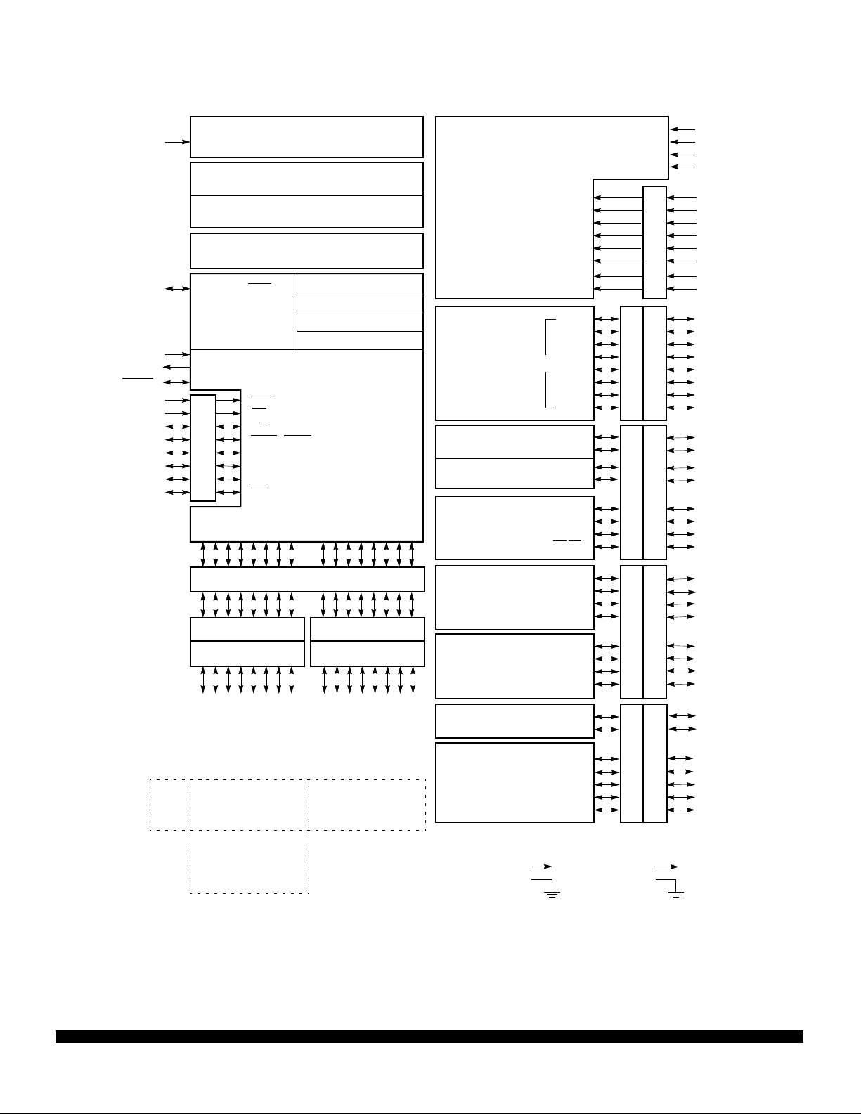
1.3 MC68HC912B32 Block Diagram
V
BKGD
EXTAL
XTAL
RESET
PE0
PE1
PE2
PE3
PE4
PE5
PE6
PE7
V
FP
32-KBYTE FLASH EEPROM
1-KBYTE RAM
AN0
768-BYTE EEPROM
SMODN / TAGHI
SINGLE-WIRE
BACKGROUND
DEBUG MODULE
XIRQ
IRQ/V
R/W
LSTRB / TAGLO
PORT E
ECLK
IPIPE0 / MODA
IPIPE1 / MODB
DBE
CPU12
PERIODIC INTERRUPT
COP WATCHDOG
CLOCK MONITOR
PP
BREAK POINTS
LITE
INTEGRATION
MODULE
(LIM)
ATD
CONVERTER
TIMER AND
PULSE
ACCUMULATOR
SCI
I/O
SPI
AN1
AN2
AN3
AN4
AN5
AN6
AN7
IOC0
IOC1
IOC2
IOC3
OC7
IOC4
IOC5
IOC6
PAI
RxD
TxD
I/O
I/O
SDI/MISO
SDO/MOSI
SCK
CS/SS
RH
V
RL
V
DDA
V
SSA
DDRT
DDRS
PORT AD
PORT T
PORT S
V
RH
V
RL
V
DDA
V
SSA
PAD0
PAD1
PAD2
PAD3
PAD4
PAD5
PAD6
PAD7
PT0
PT1
PT2
PT3
PT4
PT5
PT6
PT7
PS0
PS1
PS2
PS3
PS4
PS5
PS6
PS7
WIDE
BUS
MULTIPLEXED ADDRESS/DATA BUS
DDRA
PORT A
PA4
PA7
PA6
PA5
ADDR15
ADDR14
ADDR13
ADDR12
DATA14
DATA13
DATA12
DATA15
DATA7
DATA6
DATA5
DATA4
NARROW BUS
PA3
PA2
ADDR11
ADDR10
DATA11
DATA10
DATA3
DATA2
PA1
PA0
ADDR9
ADDR8
DATA9
DATA8
DATA1
DATA0
PB7
PB6
ADDR7
ADDR6
DATA7
DATA6
DDRB
PORT B
PB5
ADDR5
DATA5
PB4
PB3
ADDR4
ADDR3
DATA4
DATA3
PB2
PB1
ADDR2
ADDR1
DATA2
DATA1
PB0
ADDR0
DATA0
PWM
I/O
BDLC
I/O
VDD × 2
× 2
V
SS
POWER FOR
INTERNAL
CIRCUITRY
PW0
PW1
PW2
PW3
I/O
I/O
I/O
I/O
DLCRx
DLCTx
I/O
I/O
I/O
I/O
I/O
V
× 2
DDX
V
× 2
SSX
POWER FOR
I/O DRIVERS
DDRP
PORT P
DDRDLC
PORT DLC
PP0
PP1
PP2
PP3
PP4
PP5
PP6
PP7
PDLC0
PDLC1
PDLC2
PDLC3
PDLC4
PDLC5
PDLC6
Figure 1 MC68HC912B32 Block Diagram
MC68HC912B32 MOTOROLA
MC68HC912B32TS/D 5
Page 6

2 Central Processing Unit
The CPU12 is a high-speed, 16-bit processing unit. It has full 16-bit data paths and wider internal registers (up to 20 bits) for high-speed extended math instructions. The instruction set is a proper superset
of the M68HC11instruction set. The CPU12 allows instructions with odd byte counts, including many
single-byte instructions. This provides efficient use of ROM space. An instruction queue buffers program information so the CPU always has immediate access to at least three bytes of machine code at
the start of every instruction. The CPU12 also offers an extensive set of indexed addressing capabilities.
2.1 Programming Model
CPU12 registers are an integral part of the CPU and are not addressed as if they were memory locations.
15
15
15
15
15
7
AB
D
IX
IY
SP
PC
70
NSXHI ZVC
8-BIT ACCUMULATORS A & B
0
OR
16-BIT DOUBLE ACCUMULATOR D
0
INDEX REGISTER X
0
INDEX REGISTER Y
0
STACK POINTER
0
PROGRAM COUNTER
0
CONDITION CODE REGISTER
HC12 PROG MODEL
Figure 2 Programming Model
Accumulators A and B are general-purpose 8-bit accumulators used to hold operands and results of
arithmetic calculations or data manipulations. Some instructions treat the combination of these two 8bit accumulators as a 16-bit double accumulator (accumulator D).
Index registers X and Y are used for indexed addressing mode. In the indexed addressing mode, the
contents of a 16-bit index register are added to 5-bit, 9-bit, or 16-bit constants or the content of an accumulator to form the effective address of the operand to be used in the instruction.
Stack pointer (SP) points to the last stack location used. The CPU12 supports an automatic program
stack that is used to save system context during subroutine calls and interrupts, and can also be used
for temporary storage of data. The stack pointer can also be used in all indexed addressing modes.
Program counter is a 16-bit register that holds the address of the next instruction to be executed. The
program counter can be used in all indexed addressing modes except auto-increment/decrement.
Condition Code Register (CCR) contains five status indicators, two interrupt masking bits, and a
STOP disable bit. The five flags are half carry (H), negative (N), zero (Z), overflow (V), and carry/borrow
(C). The half-carry flag is used only for BCD arithmetic operations. The N, Z, V, and C status bits allow
for branching based on the results of a previous operation.
MOTOROLA MC68HC912B32
6 MC68HC912B32TS/D
Page 7

2.2 Data Types
The CPU12 supports the following data types:
• Bit data
• 8-bit and 16-bit signed and unsigned integers
• 16-bit unsigned fractions
• 16-bit addresses
A byte is eight bits wide and can be accessed at any byte location. A word is composed of two consecutive bytes with the most significant byte at the lower value address. There are no special requirements
for alignment of instructions or operands.
2.3 Addressing Modes
Addressing modes determine how the CPU accesses memory locations to be operated upon. The
CPU12 includes all of the addressing modes of the M68HC11 CPU as well as several new forms of indexed addressing. Table 2 is a summary of the available addressing modes.
Table 2 M68HC12 Addressing Mode Summary
Addressing Mode Source Format Abbreviation Description
Inherent
Immediate
Direct INST
Extended INST
Relative
Indexed
(5-bit offset)
Indexed
(auto pre-decrement)
Indexed
(auto pre-increment)
Indexed
(auto post-
decrement)
Indexed
(auto post-increment)
Indexed
(accumulator offset)
Indexed
(9-bit offset)
Indexed
(16-bit offset)
Indexed-Indirect
(16-bit offset)
Indexed-Indirect
(D accumulator
offset)
(no externally supplied
operands)
INST #
INST #
INST
INST
INST
INST
INST
INST
INST
INST
INST
INST [
INST [D,
INST
opr8i
or
opr16i
opr8a
opr16a
rel8
INST
or
rel16
oprx5,xysp
oprx3,–xys
oprx3,+xys
oprx3,xys–
oprx3,xys+
abd,xysp
oprx9,xysp
oprx16,xysp
oprx16,xysp
xysp
INH Operands (if any) are in CPU registers
IMM
DIR
EXT Operand is a 16-bit address
REL
IDX 5-bit signed constant offset from x, y, sp, or pc
IDX Auto pre-decrement x, y, or sp by 1 ~ 8
IDX Auto pre-increment x, y, or sp by 1 ~ 8
IDX Auto post-decrement x, y, or sp by 1 ~ 8
IDX Auto post-increment x, y, or sp by 1 ~ 8
IDX
IDX1
IDX2
] [IDX2]
] [D,IDX]
Operand is included in instruction stream
8- or 16-bit size implied by context
Operand is the lower 8-bits of an address in the
range $0000 – $00FF
An 8-bit or 16-bit relative offset from the current
pc is supplied in the instruction
Indexed with 8-bit (A or B) or 16-bit (D) accumu-
lator offset from x, y, sp, or pc
9-bit signed constant offset from x, y, sp, or pc
(lower 8-bits of offset in one extension byte)
16-bit constant offset from x, y, sp, or pc
(16-bit offset in two extension bytes)
Pointer to operand is found at...
16-bit constant offset from x, y, sp, or pc
(16-bit offset in two extension bytes)
Pointer to operand is found at...
x, y, sp, or pc plus the value in D
MC68HC912B32 MOTOROLA
MC68HC912B32TS/D 7
Page 8

2.4 Indexed Addressing Modes
The CPU12 indexed modes reduce execution time and eliminate code size penalties for using the Y
index register. CPU12 indexed addressing uses a postbyte plus zero, one, or two extension bytes after
the instruction opcode. The postbyte and extensions do the following tasks:
• Specify which index register is used
• Determine whether a value in an accumulator is used as an offset
• Enable automatic pre- or post-increment or decrement
• Specify use of 5-bit, 9-bit, or 16-bit signed offsets
Table 3 Summary of Indexed Operations
Postbyte
Code (xb)
Source Code
Syntax
rr0nnnnn ,r
n,r
−n,r
111rr0zs n,r
−n,r
111rr011 [n,r]
rr1pnnnn n,−r
n,+r
n,r−
n,r+
111rr1aa A,r
B,r
D,r
111rr111 [D,r]
Comments
rr; 00 = X, 01 = Y, 10 = SP, 11 = PC
5-bit constant offset n = –16 to +15
r can specify X, Y, SP, or PC
Constant offset (9- or 16-bit signed)
z- 0 = 9-bit with sign in LSB of postbyte(s) -256 < n < 255
1 = 16-bit 0 < n < 65,535
if z = s = 1, 16-bit offset indexed-indirect (see below)
r can specify X, Y, SP, or PC
16-bit offset indexed-indirect
rr can specify X, Y, SP, or PC 0 < n < 65,535
Auto pre-decrement/increment or Auto post-decrement/increment;
p = pre-(0) or post-(1), n = –8 to –1, +1 to +8
r can specify X, Y, or SP (PC not a valid choice)
+8 = 0111
…
+1 = 0000
-1 = 1111
…
-8 = 1000
Accumulator offset (unsigned 8-bit or 16-bit)
aa- 00 = A
01 = B
10 = D (16-bit)
11 = see accumulator D offset indexed-indirect
r can specify X, Y, SP, or PC
Accumulator D offset indexed-indirect
r can specify X, Y, SP, or PC
2.5 Opcodes and Operands
The CPU12 uses 8-bit opcodes. Each opcode identifies a particular instruction and associated addressing mode to the CPU. Several opcodes are required to provide each instruction with a range of addressing capabilities.
Only 256 opcodes would be available if the range of values were restricted to the number that can be
represented by 8-bit binary numbers. To expand the number of opcodes, a second page is added to the
opcode map. Opcodes on the second page are preceded by an additional byte with the value $18.
To provide additional addressing flexibility, opcodes can also be followed by a postbyte or extension
bytes. Postbytes implement certain forms of indexed addressing, transfers, exchanges, and loop primitives. Extension bytes contain additional program information such as addresses, offsets, and immediate data.
MOTOROLA MC68HC912B32
8 MC68HC912B32TS/D
Page 9
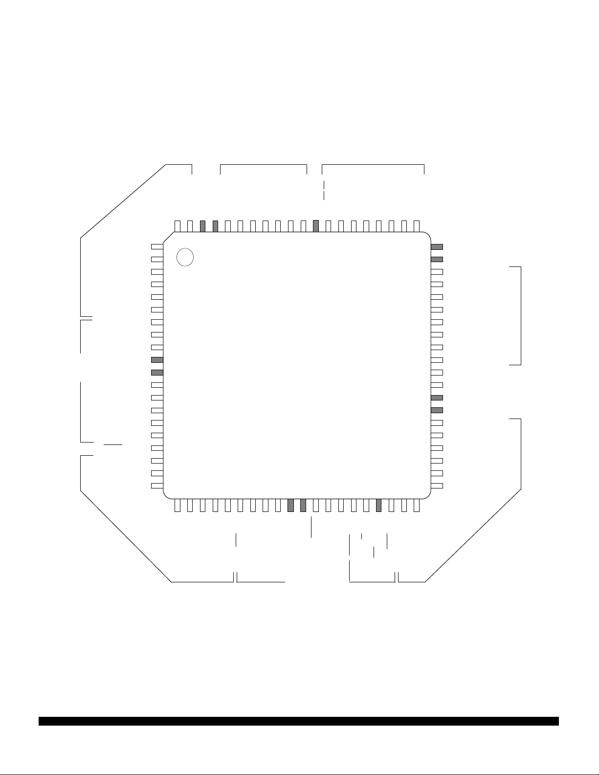
3 Pinout and Signal Descriptions
3.1 MC68HC912B32 Pin Assignments
The MC68HC912B32 is available in a 80-pin quad flat pack (QFP). Most pins perform two or more functions, as described in the 3.3 Signal Descriptions. Figure 3 shows pin assignments. Shaded pins are
power and ground.
PORT P
PW3 / PP3
PW2 / PP2
PW1/ PP1
PW0/ PP0
IOC0 / PT0
IOC1 / PT1
PORT TPORT T
SMODN / T
ADDR0 / DATA0 / PB0
ADDR1 / DATA1 / PB1
ADDR2 / DATA2 / PB2
IOC2 / PT2
IOC3 / PT3
IOC4 / PT4
IOC5 / PT5
IOC6 / PT6
PAI / IOC7 / PT7
AGHI/ BKGD
PP5
PP4
V
V
/SS
PS6 / SCK
PS7 / CS
67
68
PORT S
PS2
PS3
PS4 / SDI/MISO
PS5 / SDO/MOSI
63
64
65
66
PS1 / TxD
62
PS0 / RxD
61
V
60
59
58
57
56
55
54
53
52
51
50
49
48
47
46
45
44
43
42
41
40
SSA
V
DDA
PAD7 / AN7
PAD6 / AN6
PAD5 / AN5
PAD4 / AN4
PAD3 / AN3
PAD2 / AN2
PAD1 / AN1
PAD0 / AN0
V
RL
V
RH
V
SS
V
DD
PA7 / DATA15 / ADDR15
PA6 / DATA14 / ADDR14
PA5 / DATA13 / ADDR13
PA4 / DATA12 / ADDR12
PA3 / DATA11 / ADDR11
PA2 / DATA10 / ADDR10
PORT AD
PORT DLC
SSX
DDX
V
PP7
79
V
77
78
PDLC3
PDLC2
PDLC1 / DLCTx
PDLC0 / DLCRx
73
74
75
76
MC68HC912B32
PDLC4
72
80-PIN QFP
PP6
80
1
2
3
4
5
6
7
8
9
10
DD
11
SS
12
13
14
15
16
17
18
19
20
21222324252627282930313233343536373839
PDLC6
PDLC5
70
71
FP
V
69
SSX
DDX
PORT B
ADDR4 / DATA4 / PB4
ADDR3 / DATA3 / PB3
ADDR6 / DATA6 / PB6
ADDR5 / DATA5 / PB5
/ PE7
DBE
MODB / IPIPE1 / PE6
ADDR7 / DATA7 / PB7
V
V
ECLK / PE4
MODA / IPIPE0 / PE5
EXTAL
RESET
XTAL
/ TAGLO / PE3
LSTRB
/ PE2
R/W
/ PE1
PP
/V
IRQ
/ PE0
XIRQ
PORT A*
ADDR9 / DATA9 / PA1
ADDR8 / DATA8 / PA0
HC12 80QFP
PORT EPORT E
* In narrow mode, high and low data bytes are multiplexed in alternate bus cycles on port A.
Figure 3 Pin Assignments for MC68HC912B32
MC68HC912B32 MOTOROLA
MC68HC912B32TS/D 9
Page 10

3.2 Power Supply Pins
MC68HC912B32 power and ground pins are described below and summarized in Table 4.
3.2.1 Internal Power (VDD) and Ground (VSS)
Power is supplied to the MCU through V
and VSS. Because fast signal transitions place high, short-
DD
duration current demands on the power supply, use bypass capacitors with high-frequency characteristics and place them as close to the MCU as possible. Bypass requirements depend on how heavily
the MCU pins are loaded.
3.2.2 External Power (V
and Ground (V
DDX)
SSX
)
External power and ground for I/O drivers. Because fast signal transitions place high, short-duration current demands on the power supply, use bypass capacitors with high-frequency characteristics and
place them as close to the MCU as possible. Bypass requirements depend on how heavily the MCU
pins are loaded.
3.2.3 V
DDA
, V
SSA
Provides operating voltage and ground for the analog-to-digital converter. This allows the supply voltage to the A/D to be bypassed independently.
3.2.4 Analog-to-Digital Reference Voltages (VRH, VRL)
3.2.5 V
FP
Flash EEPROM programming voltage and supply voltage during normal operation.
3.2.6 V
PP
High voltage supply to EEPROM. Used to monitor charge pump output and testing. Not intended for
general applications use.
Table 4 MC68HC912B32 Power and Ground Connection Summary
Mnemonic Pin Number Description
V
V
V
V
V
V
V
V
V
V
DD
SS
DDX
SSX
DDA
SSA
RH
RL
FP
PP
10, 47
11, 48
31, 78
30, 77
59
60
49
50
69
37
Internal power and ground.
External power and ground, supply to pin drivers.
Operating voltage and ground for the analog-to-digital converter,
allows the supply voltage to the A/D to be bypassed independently.
Reference voltages for the analog-to-digital converter.
Programming voltage for the Flash EEPROM and required supply
for normal operation.
High voltage supply to EEPROM used for test purposes only in
special modes.
MOTOROLA MC68HC912B32
10 MC68HC912B32TS/D
Page 11
3.3 Signal Descriptions
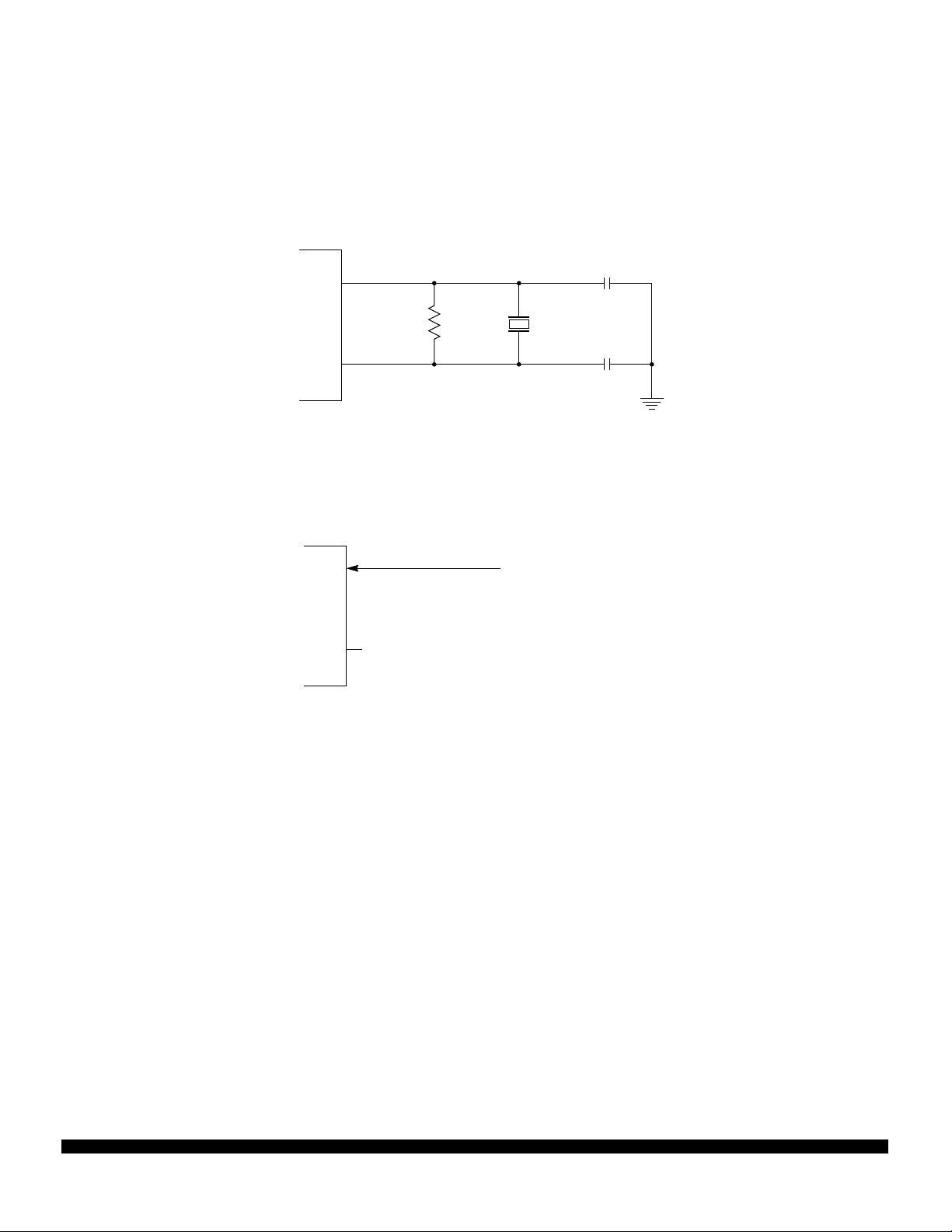
3.3.1 Crystal Driver and External Clock Input (XTAL, EXTAL)
These pins provide the interface for either a crystal or a CMOS compatible clock to control the internal
clock generator circuitry. Out of reset the frequency applied to EXTAL is twice the desired E-clock rate.
All the device clocks are derived from the EXTAL input frequency.
MCU
MCU
EXTAL
10 MΩ
XTAL
2 x E
CRYSTAL
Figure 4 Common Crystal Connections
EXTAL
XTAL
NC
CMOS-COMPATIBLE
EXTERNAL OSCILLATOR
C
C
COMMON XTAL CONN
2 x E
EXT EXTAL CONN
Figure 5 External Oscillator Connections
XTAL is the crystal output. The XTAL pin must be left unterminated when an external CMOS compatible
clock input is connected to the EXTAL pin. The XTAL output is normally intended to drive only a crystal.
The XTAL output can be buffered with a high-impedance buffer to drive the EXTAL input of another device.
In all cases take extra care in the circuit board layout around the oscillator pins. Load capacitances
shown in the oscillator circuits include all stray layout capacitances. Refer to Figure 4 and Figure 5 for
diagrams of oscillator circuits.
3.3.2 E-Clock Output (ECLK)
ECLK is the output connection for the internal bus clock and is used to demultiplex the address and data
and is used as a timing reference. ECLK frequency is equal to 1/2 the crystal frequency out of reset. Eclock output can be turned off in single-chip modes to reduce the effects of RFI. In special peripheral
mode the E clock is an input to the MCU. All clocks, including the E-clock, are halted when the MCU is
in STOP mode. It is possible to configure the MCU to interface to slow external memory. ECLK can be
stretched for such accesses.
MC68HC912B32 MOTOROLA
MC68HC912B32TS/D 11
Page 12

3.3.3 Reset (RESET)
An active low bidirectional control signal, RESET, acts as an input to initialize the MCU to a known startup state. It also acts as an open-drain output to indicate that an internal failure has been detected in
either the clock monitor or COP watchdog circuit. The MCU goes into reset asynchronously and comes
out of reset synchronously. This allows the part to reach a proper reset state even if the clocks have
failed, while allowing synchronized operation when starting out of reset.
It is possible to determine whether a reset was caused by an internal source or an external source. An
internal source drives the pin low for 16 cycles; eight cycles later the pin is sampled. If the pin has returned high, either the COP watchdog vector or clock monitor vector will be taken. If the pin is still low,
the external reset is determined to be active and the reset vector is taken. Hold reset low for at least 32
cycles to assure that the reset vector is taken in the event that an internal COP watchdog time-out or
clock monitor fail occurs.
3.3.4 Maskable Interrupt Request (IRQ
)
The IRQ input provides a means of applying asynchronous interrupt requests to the MCU. Either falling
edge-sensitive triggering or level-sensitive triggering is program selectable (INTCR register). IRQ is always configured to level-sensitive triggering at reset. When the MCU is reset the IRQ function is
masked in the condition code register.
This pin is always an input and can always be read. In special modes it can be used to apply external
EEPROM V
and erase cycles. Because the IRQ
in support of EEPROM testing. External VPP is not needed for normal EEPROM program
PP
pin is also used as an EEPROM programming voltage pin, there is
an internal resistive pull-up on the pin.
3.3.5 Nonmaskable Interrupt (XIRQ)
The XIRQ input provides a means of requesting a nonmaskable interrupt after reset initialization. During
reset, the X bit in the condition code register (CCR) is set and any interrupt is masked until MCU software enables it. Because the XIRQ input is level sensitive, it can be connected to a multiple-source
wired-OR network. This pin is always an input and can always be read. There is an active pull-up on
this pin while in reset and immediately out of reset. The pull-up can be turned off by clearing PUPE in
the PUCR register. XIRQ is often used as a power loss detect interrupt.
Whenever XIRQ or IRQ are used with multiple interrupt sources (IRQ must be configured for level-sensitive operation if there is more than one source of IRQ interrupt), each source must drive the interrupt
input with an open-drain type of driver to avoid contention between outputs. There must also be an interlock mechanism at each interrupt source so that the source holds the interrupt line low until the MCU
recognizes and acknowledges the interrupt request. If the interrupt line is held low, the MCU will recognize another interrupt as soon as the interrupt mask bit in the MCU is cleared (normally upon return from
an interrupt).
3.3.6 Mode Select (SMODN, MODA, and MODB)
The state of these pins during reset determine the MCU operating mode. After reset, MODA and MODB
can be configured as instruction queue tracking signals IPIPE0 and IPIPE1. MODA and MODB have
active pulldowns during reset.
The SMODN pin can be used as BKGD or T
AGHI after reset.
3.3.7 Single-Wire Background Mode Pin (BKGD)
The BKGD pin receives and transmits serial background debugging commands. A special self-timing
protocol is used. The BKGD pin has an active pull-up when configured as input; BKGD has no pull-up
control. Refer to 16 Development Support.
MOTOROLA MC68HC912B32
12 MC68HC912B32TS/D
Page 13

3.3.8 External Address and Data Buses (ADDR[15:0] and DATA[15:0])
External bus pins share function with general-purpose I/O ports A and B. In single-chip operating
modes, the pins can be used for I/O; in expanded modes, the pins are used for the external buses.
In expanded wide mode, ports A and B are used for multiplexed 16-bit data and address buses. PA[7:0]
correspond to ADDR[15:8]/DATA[15:8]; PB[7:0] correspond to ADDR[7:0]/DATA[7:0].
In expanded narrow mode, ports A and B are used for the 16-bit address bus, and an 8-bit data bus is
multiplexed with the most significant half of the address bus on port A. In this mode, 16-bit data is handled as two back-to-back bus cycles, one for the high byte followed by one for the low byte. PA[7:0]
correspond to ADDR[15:8] and to DATA[15:8] or DATA[7:0], depending on the bus cycle. The state of
the address pin should be latched at the rising edge of E. To allow for maximum address setup time at
external devices, a transparent latch should be used.
3.3.9 Read/Write (R/W
In all modes this pin can be used as I/O and is a general-purpose input with an active pull-up out of
reset. If the read/write function is required it should be enabled by setting the RDWE bit in the PEAR
register. External writes will not be possible until enabled.
3.3.10 Low-Byte Strobe (LSTRB)
In all modes this pin can be used as I/O and is a general-purpose input with an active pull-up out of
reset. If the strobe function is required, it should be enabled by setting the LSTRE bit in the PEAR register. This signal is used in write operations and so external low byte writes will not be possible until this
function is enabled. This pin is also used as TAGLO in special expanded modes and is multiplexed with
the LSTRB function.
3.3.11 Instruction Queue Tracking Signals (IPIPE1 and IPIPE0)
These signals are used to track the state of the internal instruction execution queue. Execution state is
time-multiplexed on the two signals. Refer to 16 Development Support.
3.3.12 Data Bus Enable (DBE)
The DBE pin (PE7) is an active low signal that will be asserted low during E-clock high time. DBE provides separation between output of a multiplexed address and the input of data. When an external address is stretched, DBE is asserted during what would be the last quarter cycle of the last E-clock cycle
of stretch. In expanded modes this pin is used to enable the drive control of external buses during external reads. Use of the DBE is controlled by the NDBE bit in the PEAR register. DBE is enabled out of
reset in expanded modes. This pin has an active pull-up during and after reset in single-chip modes.
)
MC68HC912B32 MOTOROLA
MC68HC912B32TS/D 13
Page 14
Table 5 MC68HC912B32 Signal Description Summary
Pin Name Pin Number Description
PW[3:0] 3–6 Pulse Width Modulator channel outputs.
ADDR[7:0]
DATA[7:0]
ADDR[15:8]
DATA[15:8]
IOC[7:0] 16–12, 9–7
PAI 16 Pulse accumulator input
AN[7:0] 58–51 Analog inputs for the analog-to-digital conversion module
DBE
MODB, MODA 27, 28 State of mode select pins during reset determine the initial operating mode of the
IPIPE1, IPIPE0 27, 28
ECLK 29
RESET 32
EXTAL 33
XTAL 34
LSTRB
AGLO 35 Pin used in instruction tagging. See 16 Development Support.
T
R/W
IRQ 37
XIRQ 38
BKGD 17
AGHI 17 Pin used in instruction tagging. See 16 Development Support.
T
DLCRx 76 BDLC receive pin
DLCTx 75 BDLC transmit pin
/SS 68 Slave select output for SPI master mode, input for slave mode or master mode.
CS
SCK 67 Serial clock for SPI system.
SDO/MOSI 66 Master out/slave in pin for serial peripheral interface
SDI/MISO 65 Master in/slave out pin for serial peripheral interface
TxD0 62 SCI transmit pin
RxD0 61 SCI receive pin
25–18
46–39
26
35
36
External bus pins share function with general-purpose I/O ports A and B. In single chip modes, the pins can be used for I/O. In expanded modes, the pins are
used for the external buses.
Pins used for input capture and output compare in the timer and pulse accumulator subsystem.
Data bus control and, in expanded mode, enables the drive control of external
buses during external reads.
MCU. After reset, MODB and MODA can be configured as instruction queue
tracking signals IPIPE1 and IPIPE0 or as general-purpose I/O pins.
E-clock is the output connection for the external bus clock. ECLK is used as a
timing reference and for address demultiplexing.
An active low bidirectional control signal, RESET
MCU to a known start-up state, and an output when COP or clock monitor causes
a reset.
Crystal driver and external clock input pins. On reset all the device clocks are derived from the EXTAL input frequency. XTAL is the crystal output.
Low byte strobe (0 = low byte valid), in all modes this pin can be used as I/O. The
low strobe function is the exclusive-NOR of A0 and the internal SZ8 signal. (The
SZ8
internal signal indicates the size 16/8 access.)
Indicates direction of data on expansion bus. Shares function with general-purpose I/O. Read/write in expanded modes.
Maskable interrupt request input provides a means of applying asynchronous interrupt requests to the MCU. Either falling edge-sensitive triggering or level-sensitive triggering is program selectable (INTCR register).
Provides a means of requesting asynchronous non-maskable interrupt requests
after reset initialization.
Single-wire background interface pin is dedicated to the background debug function. During reset, this pin determines special or normal operating mode.
acts as an input to initialize the
MOTOROLA MC68HC912B32
14 MC68HC912B32TS/D
Page 15

3.4 Port Signals
The MC68HC912B32 incorporates eight ports which are used to control and access the various device
subsystems. When not used for these purposes, port pins may be used for general-purpose I/O. In addition to the pins described below, each port consists of a data register which can be read and written
at any time, and, with the exception of port AD and PE[1:0], a data direction register which controls the
direction of each pin. After reset all port pins are configured as input.
3.4.1 Port A
Port A pins are used for address and data in expanded modes. The port data register is not in the address map during expanded and peripheral mode operation. When it is in the map, port A can be read
or written at anytime.
Register DDRA determines whether each port A pin is an input or output. DDRA is not in the address
map during expanded and peripheral mode operation. Setting a bit in DDRA makes the corresponding
bit in port A an output; clearing a bit in DDRA makes the corresponding bit in port A an input. The default
reset state of DDRA is all zeros.
When the PUPA bit in the PUCR register is set, all port A input pins are pulled up internally by an active
pull-up device. This bit has no effect if the port is being used in expanded modes as the pull-ups are
inactive.
Setting the RDPA bit in register RDRIV causes all port A outputs to have reduced drive level. RDRIV
can be written once after reset. RDRIV is not in the address map in peripheral mode. Refer to 6 Bus
Control and Input/Output.
3.4.2 Port B
Port B pins are used for address and data in expanded modes. The port data register is not in the address map during expanded and peripheral mode operation. When it is in the map, port B can be read
or written at anytime.
Register DDRB determines whether each port B pin is an input or output. DDRB is not in the address
map during expanded and peripheral mode operation. Setting a bit in DDRB makes the corresponding
bit in port B an output; clearing a bit in DDRB makes the corresponding bit in port B an input. The default
reset state of DDRB is all zeros.
When the PUPB bit in the PUCR register is set, all port B input pins are pulled up internally by an active
pull-up device. This bit has no effect if the port is being used in expanded modes as the pull-ups are
inactive.
Setting the RDPB bit in register RDRIV causes all port B outputs to have reduced drive level. RDRIV
can be written once after reset. RDRIV is not in the address map in peripheral mode. Refer to 6 Bus
Control and Input/Output.
3.4.3 Port E
Port E pins operate differently from port A and B pins. Port E pins are used for bus control signals and
interrupt service request signals. When a pin is not used for one of these specific functions, it can be
used as general-purpose I/O. However, two of the pins (PE[1:0]) can only be used for input, and the
states of these pins can be read in the port data register even when they are used for IRQ
The PEAR register determines pin function, and register DDRE determines whether each pin is an input
or output when it is used for general-purpose I/O. PEAR settings override DDRE settings. Because
PE[1:0] are input-only pins, only DDRE[7:2] have effect. Setting a bit in the DDRE register makes the
corresponding bit in port E an output; clearing a bit in the DDRE register makes the corresponding bit
in port E an input. The default reset state of DDRE is all zeros.
and XIRQ.
MC68HC912B32 MOTOROLA
MC68HC912B32TS/D 15
Page 16

When the PUPE bit in the PUCR register is set, PE[7,3,2,0] are pulled up. PE[7,3,2,0] are pulled up active devices, while PE1 is always pulled up by means of an internal resistor.
Neither port E nor DDRE is in the map in peripheral mode; neither is in the internal map in expanded
modes with EME set.
Setting the RDPE bit in register RDRIV causes all port E outputs to have reduced drive level. RDRIV
can be written once after reset. RDRIV is not in the address map in peripheral mode. Refer to 6 Bus
Control and Input/Output.
3.4.4 Port DLC
BDLC pins can be configured as general-purpose I/O port DLC. When BDLC functions are not enabled,
the port has seven general-purpose I/O pins, PDLC[6:0]. The DLCSCR register controls port DLC function. The BDLC function, enabled with the BDLCEN bit, takes precedence over other port functions.
Register DDRDLC determines whether each port DLC pin is an input or output. Setting a bit in DDRDLC
makes the corresponding pin in port DLC an output; clearing a bit makes the corresponding pin an input.
After reset port DLC pins are configured as inputs.
When the PUPDLC bit in the DLCSCR register is set, all port DLC input pins are pulled up internally by
an active pull-up device.
Setting the RDPDLC bit in register DLCSCR causes all port DLC outputs to have reduced drive level.
Levels are at normal drive capability after reset. RDPDLC can be written anytime after reset. Refer to
14 Byte Data Link Communications Module (BDLC).
3.4.5 Port AD
Input to the analog-to-digital subsystem and general-purpose input. When analog-to-digital functions
are not enabled, the port has eight general-purpose input pins, P AD[7:0]. The ADPU bit in the ATDCTL2
register enables the A/D function.
Port AD pins are inputs; no data direction register is associated with this port. The port has no resistive
input loads and no reduced drive controls. Refer to 15 Analog-To-Digital Converter.
3.4.6 Port P
The four pulse-width modulation channel outputs share general-purpose port P pins. The PWM function
is enabled with the PWEN register. Enabling PWM pins takes precedence over the general-purpose
port. When pulse-width modulation is not in use, the port pins may be used for general-purpose I/O.
Register DDRP determines pin direction of port P when used for general-purpose I/O. When DDRP bits
are set, the corresponding pin is configured for output. On reset the DDRP bits are cleared and the corresponding pin is configured for input.
When the PUPP bit in the PWCTL register is set, all input pins are pulled up internally by an active pullup device. Pull-ups are disabled after reset.
Setting the RDPP bit in the PWCTL register configures all port P outputs to have reduced drive levels.
Levels are at normal drive capability after reset. The PWCTL register can be read or written anytime
after reset. Refer to 11 Pulse-Width Modulator.
3.4.7 Port T
This port provides eight general-purpose I/O pins when not enabled for input capture and output compare in the timer and pulse accumulator subsystem. The TEN bit in the TSCR register enab les the timer
function. The pulse accumulator subsystem is enabled with the PAEN bit in the PACTL register.
MOTOROLA MC68HC912B32
16 MC68HC912B32TS/D
Page 17

Register DDRT determines pin direction of port T when used for general-purpose I/O. When DDRT bits
are set, the corresponding pin is configured for output. On reset the DDRT bits are cleared and the corresponding pin is configured for input.
When the PUPT bit in the TMSK2 register is set, all input pins are pulled up internally by an active pullup device. Pull-ups are disabled after reset.
Setting the RDPT bit in the TMSK2 register configures all port T outputs to have reduced drive levels.
Levels are at normal drive capability after reset. The TMSK2 register can be read or written anytime
after reset. Refer to 12 Standard Timer Module.
3.4.8 Port S
Port S is the 8-bit interface to the standard serial interface consisting of the serial communications interface (SCI) and serial peripheral interface (SPI) subsystems. Port S pins are available for general-purpose parallel I/O when standard serial functions are not enabled.
Port S pins serve several functions depending on the various internal control registers. If WOMS bit in
the SC0CR1 register is set, the P-channel drivers of the output buffers are disabled for bits 0 through 1
(2 through 3). If SWOM bit in the SP0CR1 register is set, the P-channel drivers of the output buffers are
disabled for bits 4 through 7. (wired-OR mode). The open drain control effects both the serial and the
general-purpose outputs. If the RDPSx bits in the PURDS register are set, the appropriate port S pin
drive capabilities are reduced. If PUPSx bits in the PURDS register are set, the appropriate pull-up device is connected to each port S pin which is programmed as a general-purpose input . If the pin is programmed as a general-purpose output, the pull-up is disconnected from the pin regardless of the state
of the individual PUPSx bits. See 13 Serial Interface.
MC68HC912B32 MOTOROLA
MC68HC912B32TS/D 17
Page 18

Table 6 MC68HC912B32 Port Description Summary
Port Name
Port A
PA[7:0]
Port B
PB[7:0]
Port AD
PAD[7:0]
Port DLC
PDLC[6:0]
Port E
PE[7:0]
Port P
PP[7:0]
Port S
PS[7:0]
Port T
PT[7:0]
Pin
Numbers
46–39
25–18
58–51 In Analog-to-digital converter and general-purpose I/O.
70–76
26–29, 35–38
79, 80, 1–6
68–61
16–12, 9–7
Data Direction
DD Register (Address) Description
In/Out
DDRA ($0002)
In/Out
DDRB ($0003)
In/Out
DDRDLC ($00FF)
PE[1:0] In
PE[7:2] In/Out
DDRE ($0009)
In/Out
DDRP ($0057)
In/Out
DDRS ($00D7)
In/Out
DDRT ($00AF)
Port A and port B pins are used for address and data in expanded modes. The port data registers are not in the address
map during expanded and peripheral mode operation. When
in the map, port A and port B can be read or written any time.
DDRA and DDRB are not in the address map in expanded or
peripheral modes.
Byte Data Link Communication (BDLC) subsystem and
general-purpose I/O.
Mode selection, bus control signals and interrupt service
request signals; or general-purpose I/O.
General-purpose I/O. PP[3:0] are use with the pulse-width
modulator when enabled.
Serial communications interface and serial peripheral interface subsystems and general-purpose I/O.
General-purpose I/O when not enabled for input capture and
output compare in the timer and pulse accumulator subsystem.
MOTOROLA MC68HC912B32
18 MC68HC912B32TS/D
Page 19

3.5 Port Pull-Up, Pull-Down and Reduced Drive
MCU ports can be configured for internal pull-up. To reduce power consumption and RFI, the pin output
drivers can be configured to operate at a reduced drive level. Reduced drive causes a slight increase
in transition time depending on loading and should be used only for ports which have a light loading.
Table 7 summarizes the port pull-up default status and controls.
Table 7 Port Pull-Up, Pull-Down and Reduced Drive Summary
Enable Bit Reduced Drive Control Bit
Port
Name
Port A Pull-up PUCR ($000C) PUPA Disabled RDRIV ($000D) RDPA Full Drive
Port B Pull-up PUCR ($000C) PUPB Disabled RDRIV ($000D) RDPB Full Drive
Port E:
PE7, PE3,
PE2, PE0
PE1 Pull-up Always Enabled RDRIV ($000D) RDPE Full Drive
PE[6:4] None — RDRIV ($000D) RDPE Full Drive
PE[6:5] Pull-down Enabled During Reset — — —
Port P Pull-up PWCTL ($0054) PUPP Disabled PWCTL ($0054) RDPP Full Drive
Port S Pull-up PURDS ($00DB) PUPS0 Disabled PURDS ($00DB) RDPS0 Full Drive
PS[3:2] Pull-up PURDS ($00DB) PUPS1 Disabled PURDS ($00DB) RDPS1 Full Drive
PS[7:4] Pull-up PURDS ($00DB) PUPS2 Disabled PURDS ($00DB) RDPS2 Full Drive
Port T Pull-up TMSK2 ($008D) PUPT Disabled TMSK2 ($008D) RDPT Full Drive
Port DLC Pull-up DLCSCR ($00FD) DLCPUE Disabled DLCSCR ($00FD) DLCRDV Full Drive
Port AD None — —
BKGD Pull-up — — Enabled — — Full Drive
Resistive
Input Loads
Pull-up PUCR ($000C) PUPE Enabled RDRIV ($000D) RDPE Full Drive
Register
(Address)
Bit Name Reset State
Register
(Address)
Bit Name
Reset
State
MC68HC912B32 MOTOROLA
MC68HC912B32TS/D 19
Page 20

4 Register Block
The register block can be mapped to any 2-Kbyte boundary within the standard 64-Kbyte address space
by manipulating bits REG[15:11] in the INITRG register. INITRG establishes the upper five bits of the
register block’s 16-bit address. The register block occupies the first 512 bytes of the 2-Kbyte block. Default addressing (after reset) is indicated in the table below. For additional information refer to 5 Oper-
ating Modes and Resource Mapping.
Table 8 MC68HC912B32 Register Map (Sheet 1 of 5)
Address Bit 7 65432 1Bit 0 Name
$0000 PA7 PA6 PA5 PA4 PA3 PA2 PA1 PA0 PORTA
$0001 PB7 PB6 PB5 PB4 PB3 PB2 PB1 PB0
$0002 DDA7 DDA6 DDA5 DDA4 DDA3 DDA2 DDA1 DDA0
$0003 DDB7 DDB6 DDB5 DDB4 DDB3 DDB2 DDB1 DDB0
$0004 000000 00Reserved
$0005 000000 00Reserved
$0006 000000 00Reserved
$0007 000000 00Reserved
$0008 PE7 PE6 PE5 PE4 PE3 PE2 PE1 PE0 PORTE
$0009 DDE7 DDE6 DDE5 DDE4 DDE3 DDE2 0 0
$000A NDBE 0 PIPOE NECLK LSTRE RDWE 0 0
$000B SMODN MODB MODA ESTR IVIS EBSWAI 0 EME MODE
$000C 0 0 0 PUPE 0 0 PUPB PUPA
$000D 0000RDPE 0 RDPB RDPA
$000E 000000 0 0Reserved
$000F 000000 0 0Reserved
$0010 RAM15 RAM14 RAM13 RAM12 RAM11 0 0 0 INITRM
$0011 REG15 REG14 REG13 REG12 REG11 0 0 MMSWAI INITRG
$0012 EE15 EE14 EE13 EE12 0 0 0 EEON INITEE
$0013 0 NDRF RFSTR1 RFSTR0 EXSTR1 EXSTR0 MAPROM ROMON MISC
$0014 RTIE RSWAI RSBCK 0 RTBYP RTR2 RTR1 RTR0 RTICTL
$0015 RTIF 000000 0RTIFLG
$0016 CME FCME FCM FCOP DISR CR2 CR1 CR0 COPCTL
$0017 Bit 7 654321Bit 0 COPRST
$0018 ITE6 ITE8 ITEA ITEC ITEE ITF0 ITF2 ITF4 ITST0
$0019 ITD6 ITD8 ITDA ITDC ITDE ITE0 ITE2 ITE4 ITST1
$001A ITC6 ITC8 ITCA ITCC ITCE ITD0 ITD2 ITD4 ITST2
$001B 00000ITC0 ITC2 ITC4 ITST3
$001C–
$001D
000000 0 0Reserved
$001E IRQE IRQEN DLY 0 0 0 0 0 INTCR
$001F 1 1 PSEL5 PSEL4 PSEL3 PSEL2 PSEL1 0 HPRIO
$0020 BKEN1 BKEN0 BKPM 0 BK1ALE BK0ALE 0 0 BRKCT0
$0021 0 BKDBE BKMBH BKMBL BK1RWE BK1RW BK0RWE BK0RW BRKCT1
$0022 Bit 15 14 13 12 11 10 9 Bit 8 BRKAH
PORTB
DDRA
DDRB
DDRE
PEAR
PUCR
RDRIV
1
1
1
1
2
2
2
3
3
3
MOTOROLA MC68HC912B32
20 MC68HC912B32TS/D
Page 21

Table 8 MC68HC912B32 Register Map (Sheet 2 of 5)
Address Bit 7 65432 1Bit 0 Name
$0023 Bit 7 654321Bit 0 BRKAL
$0024 Bit 15 14 13 12 11 10 9 Bit 8 BRKDH
$0025 Bit 7 654321Bit 0 BRKDL
$0026–
$003F
$0040 CON23 CON01 PCKA2 PCKA1 PCKA0 PCKB2 PCKB1 PCKB0 PWCLK
$0041 PCLK3 PCLK2 PCLK1 PCLK0 PPOL3 PPOL2 PPOL1 PPOL0 PWPOL
$0042 0000PWEN3 PWEN2 PWEN1 PWEN0 PWEN
$0043 Bit 7 654321Bit 0 PWPRES
$0044 Bit 7 654321Bit 0 PWSCAL0
$0045 Bit 7 654321Bit 0 PWSCNT0
$0046 Bit 7 654321Bit 0 PWSCAL1
$0047 Bit 7 654321Bit 0 PWSCNT1
$0048 Bit 7 654321Bit 0 PWCNT0
$0049 Bit 7 654321Bit 0 PWCNT1
$004A Bit 7 65432 1Bit 0 PWCNT2
$004B Bit 7 65432 1Bit 0 PWCNT3
$004C Bit 7 65432 1Bit 0 PWPER0
$004D Bit 7 65432 1Bit 0 PWPER1
$004E Bit 7 65432 1Bit 0 PWPER2
$004F Bit 7 65432 1Bit 0 PWPER3
$0050 Bit 7 654321Bit 0 PWDTY0
$0051 Bit 7 654321Bit 0 PWDTY1
$0052 Bit 7 654321Bit 0 PWDTY2
$0053 Bit 7 654321Bit 0 PWDTY3
$0054 0 0 0 PSWAI CENTR RDPP PUPP PSBCK PWCTL
$0055 DISCR DISCP DISCAL 0 0 0 0 0 PWTST
$0056 PP7 PP6 PP5 PP4 PP3 PP2 PP1 PP0 PORTP
$0057 DDP7 DDP6 DDP5 DDP4 DDP3 DDP2 DDP1 DDP0 DDRP
$0058–
$005F
$0060 000000 0 0ATDCTL0
$0061 000000 0 0ATDCTL1
$0062 ADPU AFFC ASWAI 0 0 0 ASCIE ASCIF ATDCTL2
$0063 000000FRZ1 FRZ0 ATDCTL3
$0064 0 SMP1 SMP0 PRS4 PRS3 PRS2 PRS1 PRS0 ATDCTL4
$0065 0 S8CM SCAN MULT CD CC CB CA ATDCTL5
$0066 SCF 0000CC2CC1CC0ATDSTAT
$0067 CCF7 CCF6 CCF5 CCF4 CCF3 CCF2 CCF1 CCF0 ATDSTAT
$0068 SAR9 SAR8 SAR7 SAR6 SAR5 SAR4 SAR3 SAR2 ATDTSTH
$0069 SAR1 SAR0 RST TSTOUT TST3 TST2 TST1 TST0 ATDTSTL
$006A–
$006E
000000 0 0Reserved
000000 0 0Reserved
000000 0 0Reserved
MC68HC912B32 MOTOROLA
MC68HC912B32TS/D 21
Page 22

Table 8 MC68HC912B32 Register Map (Sheet 3 of 5)
Address Bit 7 65432 1Bit 0 Name
$006F PAD7 PAD6 PAD5 PAD4 PAD3 PAD2 PAD1 PAD0 PORTAD
$0070 Bit 7 654321Bit 0 ADR0H
$0071 000000 0 0Reserved
$0072 Bit 7 654321Bit 0 ADR1H
$0073 000000 0 0Reserved
$0074 Bit 7 654321Bit 0 ADR2H
$0075 000000 0 0Reserved
$0076 Bit 7 654321Bit 0 ADR3H
$0077 000000 0 0Reserved
$0078 Bit 7 654321Bit 0 ADR4H
$0079 000000 0 0Reserved
$007A Bit 7 65432 1Bit 0 ADR5H
$007B 000000 0 0Reserved
$007C Bit 7 65432 1Bit 0 ADR6H
$007D 000000 0 0Reserved
$007E Bit 7 65432 1Bit 0 ADR7H
$007F 000000 0 0Reserved
$0080 IOS7 IOS6 IOS5 IOS4 IOS3 IOS2 IOS1 IOS0 TIOS
$0081 FOC7 FOC6 FOC5 FOC4 FOC3 FOC2 FOC1 FOC0 CFORC
$0082 OC7M7 OC7M6 OC7M5 OC7M4 OC7M3 OC7M2 OC7M1 OC7M0 OC7M
$0083 OC7D7 OC7D6 OC7D5 OC7D4 OC7D3 OC7D2 OC7D1 OC7D0 OC7D
$0084 Bit 15 14 13 12 11 10 9 Bit 8 TCNT (H)
$0085 Bit 7 654321Bit 0 TCNT (L)
$0086 TEN TSWAI TSBCK TFFCA 0 0 0 0 TSCR
$0087 000000 0 0TQCR
$0088 OM7 OL7 OM6 OL6 OM5 OL5 OM4 OL4 TCTL1
$0089 OM3 OL3 OM2 OL2 OM1 OL1 OM0 OL0 TCTL2
$008A EDG7B EDG7A EDG6B EDG6A EDG5B EDG5A EDG4B EDG4A TCTL3
$008B EDG3B EDG3A EDG2B EDG2A EDG1B EDG1A EDG0B EDG0A TCTL4
$008C C7I C6I C5I C4I C3I C2I C1I C0I TMSK1
$008D TOI 0 PUPT RDPT TCRE PR2 PR1 PR0 TMSK2
$008E C7F C6F C5F C4F C3F C2F C1F C0F TFLG1
$008F TOF 00000 0 0TFLG2
$0090 Bit 15 14 13 12 11 10 9 Bit 8 TC0 (H)
$0091 Bit 7 654321Bit 0 TC0 (L)
$0092 Bit 15 14 13 12 11 10 9 Bit 8 TC1 (H)
$0093 Bit 7 654321Bit 0 TC1 (L)
$0094 Bit 15 14 13 12 11 10 9 Bit 8 TC2 (H)
$0095 Bit 7 654321Bit 0 TC2 (L)
$0096 Bit 15 14 13 12 11 10 9 Bit 8 TC3 (H)
$0097 Bit 7 654321Bit 0 TC3 (L)
$0098 Bit 15 14 13 12 11 10 9 Bit 8 TC4 (H)
MOTOROLA MC68HC912B32
22 MC68HC912B32TS/D
Page 23

Table 8 MC68HC912B32 Register Map (Sheet 4 of 5)
Address Bit 7 65432 1Bit 0 Name
$0099 Bit 7 654321Bit 0 TC4 (L)
$009A Bit 15 14 13 12 11 10 9 Bit 8 TC5 (H)
$009B Bit 7 65432 1Bit 0 TC5 (L)
$009C Bit 15 14 13 12 11 10 9 Bit 8 TC6 (H)
$009D Bit 7 65432 1Bit 0 TC6 (L)
$009E Bit 15 14 13 12 11 10 9 Bit 8 TC7 (H)
$009F Bit 7 65432 1Bit 0 TC7 (L)
$00A0 0 PAEN PAMOD PEDGE CLK1 CLK0 PAOVI PAI PACTL
$00A1 000000PAOVF PAIF PAFLG
$00A2 Bit 15 14 13 12 11 10 9 Bit 8 PACNT
$00A3 Bit 7 65432 1Bit 0 PACNT
$00A4–
$00AC
$00AD 000000TCBYP PCBYP TIMTST
$00AE PT7 PT6 PT5 PT4 PT3 PT2 PT1 PT0 PORTT
$00AF DDT7 DDT6 DDT5 DDT4 DDT3 DDT2 DDT1 DDT0 DDRT
$00B0–
$00BF
$00C0 BTST BSPL BRLD SBR12 SBR11 SBR10 SBR9 SBR8 SC0BDH
$00C1 SBR7 SBR6 SBR5 SBR4 SBR3 SBR2 SBR1 SBR0 SC0BDL
$00C2 LOOPS WOMS RSRC M WAKE ILT PE PT SC0CR1
$00C3 TIE TCIE RIE ILIE TE RE RWU SBK SC0CR2
$00C4 TDRE TC RDRF IDLE OR NF FE PF SC0SR1
$00C5 000000 0RAFSC0SR2
$00C6 R8 T8 0 0 0 0 0 0 SC0DRH
$00C7 R7/T7 R6/T6 R5/T5 R4/T4 R3/T3 R2/T2 R1/T1 R0/T0 SC0DRL
$00C8–
$00CF
$00D0 SPIE SPE SWOM MSTR CPOL CPHA SSOE LSBF SP0CR1
$00D1 000000SSWAI SPC0 SP0CR2
$00D2 00000SPR2 SPR1 SPR0 SP0BR
$00D3 SPIF WCOL 0 MODF 0 0 0 0 SP0SR
$00D4 000000 0
$00D5 Bit 7 65432 1Bit 0 SP0DR
$00D6 PS7 PS6 PS5 PS4 PS3 PS2 PS1 PS0 PORTS
$00D7 DDS7 DDS6 DDS5 DDS4 DDS3 DDS2 DDS1 DDS0 DDRS
$00D8–
$00DA
$00DB 0 RDPS2 RDPS1 RDPS0 0 PUPS2 PUPS1 PUPS0 PURDS
$00DC–
$00EF
$00F0 11111EESWAI PROTLCK EERC EEMCR
$00F1 1 1 1 BPROT4 BPROT3 BPROT2 BPROT1 BPROT0 EEPROT
000000 0 0Reserved
000000 0 0Reserved
000000 0 0Reserved
0 Reserved
000000 0 0Reserved
000000 0 0
Reserved
MC68HC912B32 MOTOROLA
MC68HC912B32TS/D 23
Page 24

Table 8 MC68HC912B32 Register Map (Sheet 5 of 5)
Address Bit 7 65432 1Bit 0 Name
$00F2 EEODD EEVEN MARG EECPD EECPRD 0 EECPM 0 EETST
$00F3 BULKP 0 0 BYTE ROW ERASE EELAT EEPGM EEPROG
$00F4 000000 0LOCK FEELCK
$00F5 000000 0BOOTP FEEMCR
$00F6 FSTE GADR HVT FENLV FDISVFP VTCK STRE MWPR FEETST
$00F7 0 0 0 FEESWAI SVFP ERAS LAT ENPE FEECTL
$00F8 IMSG CLKS R1 R0 0 0 IE WCM BCR1
$00F9 0 0 I3 I2 I1 I0 0 0 BSVR
$00FA ALOOP DLOOP RX4XE NBFS TEOD TSIFR TMIFR1 TMIFR0 BCR2
$00FB D7 D6 D5 D4 D3 D2 D1 D0 BDR
$00FC ATE RXPOL 0 0 BO3 BO2 BO1 BO0 BARD
$00FD 00000BDLCEN DLCPUE DLCRDV DLCSCR
$00FE 0 PDLC6 PDLC5 PDLC4 PDLC3 PDLC2 PDLC1 PDLC0 PORTDLC
$00FF 0 DDDLC6 DDDLC5 DDDLC4 DDDLC3 DDDLC2 DDDLC1 DDDLC0 DDRDLC
$0100–
$01FF
NOTES:
1. Port A, port B, and data direction registers DDRA and DDRB are not in map in expanded and peripheral modes.
2. Port E and DDRE not in map in peripheral mode; also not in map in expanded modes with EME set.
3. Not in map in peripheral mode.
000000 0 0Reserved
MOTOROLA MC68HC912B32
24 MC68HC912B32TS/D
Page 25

5 Operating Modes and Resource Mapping
Eight possible operating modes determine the operating configuration of the MC68HC912B32. Each
mode has an associated default memory map and external bus configuration. After reset, most system
resources can be mapped to other addresses by writing to the appropriate control registers.
5.1 Operating Modes
The operating mode out of reset is determined by the states of the BKGD, MODB, and MODA pins during reset.
The SMODN, MODB, and MODA bits in the MODE register show current operating mode and provide
limited mode switching during operation. The states of the BKGD, MODB, and MODA pins are latched
into these bits on the rising edge of the reset signal. During reset an active pull-up is connected to the
BKGD pin (as input) and active pulldowns are connected to the MODB and MODA pins. If an open occurs on any of these pins, the device will operate in normal single-chip mode.
Table 9 Mode Selection
BKGD MODB MODA Mode Port A Port B
0 0 0 Special Single Chip General-Purpose I/O General-Purpose I/O
0 0 1 Special Expanded Narrow ADDR[15:8]/DATA[15:0] ADDR[7:0]
0 1 0 Special Peripheral ADDR/DATA ADDR/DATA
0 1 1 Special Expanded Wide ADDR/DATA ADDR/DATA
1 0 0 Normal Single Chip General-Purpose I/O General-Purpose I/O
1 0 1 Normal Expanded Narrow ADDR[15:8]/DATA[15:0] ADDR[7:0]
1 1 0 Reserved (Forced to Peripheral) — —
1 1 1 Normal Expanded Wide ADDR/DATA ADDR/DATA
There are two basic types of operating modes:
Normal
modes — some registers and bits are protected against accidental changes.
Special modes — allow greater access to protected control registers and bits for special purposes such
as testing and emulation.
A system development and debug feature, background debug mode (BDM), is available in all modes.
In special single-chip mode, BDM is active immediately after reset.
5.1.1 Normal Operating Modes
These modes provide three operating configurations. Background debugging is available in all three
modes, but must first be enabled for some operations by means of a BDM command. BDM can then be
made active by another BDM command.
Normal Expanded Wide Mode — This is a normal mode of operation in which the address and data
are multiplexed onto ports A and B. ADDR[15:8] and DATA[15:8] are present on port A. ADDR[7:0] and
DATA[7:0] are present on port B.
Normal Expanded Narrow Mode — Port A is configured as the high byte of address multiplexed with
the 8-bit data bus. Port B is configured as the lower 8-bit address bus. This mode is used for lower cost
production systems that use 8-bit wide external EEPROMs or RAMs. Such systems take extra bus cycles to access 16-bit locations but this may be preferred over the extra cost of additional external memory devices.
MC68HC912B32 MOTOROLA
MC68HC912B32TS/D 25
Page 26

Normal Single-Chip Mode — There are no external address and data buses in this mode. All pins of
ports A, B and E are configured as general-purpose I/O pins. Port E bits 1 and 0 are input-only with
internal pull-ups and the other 22 pins are bidirectional I/O pins that are initially configured as high-impedance inputs. Port E pull-ups are enabled upon reset; port A and B pull-ups are disabled upon reset.
5.1.2 Special Operating Modes
There are three special operating modes that correspond to normal operating modes. These operating
modes are commonly used in factory testing and system development. In addition, there is a special
peripheral mode, in which an external master, such as an I.C. tester, can control the on-chip peripherals.
Special Expanded Wide Mode — This mode can be used for emulation of normal expanded wide
mode and emulation of normal single-chip mode and 16-bit data bus. The bus control related pins in
PORTE are all configured to serve their bus control output functions rather than general-purpose I/O.
Special Expanded Narrow Mode — This mode can be used for emulation of normal expanded narrow
mode. In this mode external 16-bit data is handled as two back-to-back bus cycles, one for the high byte
followed by one for the low byte. Internal operations continue to use full 16-bit data paths.
Special Single-Chip Mode — This mode can be used to force the MCU to active BDM mode to allow
system debug through the BKGD pin. The MCU does not fetch the reset vector and execute application
code as it would in other modes. Instead, the active background mode is in control of CPU execution
and BDM firmware is waiting for additional serial commands through the BKGD pin. There are no external address and data buses in this mode. The MCU operates as a stand-alone device and all program
and data space are on-chip. External port pins can be used for general-purpose I/O.
Special Peripheral Mode — The CPU is not active in this mode. An external master can control onchip peripherals for testing purposes. It is not possible to change to or from this mode without going
through reset. Background debugging should not be used while the MCU is in special peripheral mode
as internal bus conflicts between BDM and the external master can cause improper operation of both
modes.
5.2 Background Debug Mode
Background debug mode (BDM) is an auxiliary operating mode that is used for system development.
BDM is implemented in on-chip hardware and provides a full set of debug operations. Some BDM commands can be executed while the CPU is operating normally. Other BDM commands are firmware
based, and require the BDM firmware to be enabled and active for execution.
In special single-chip mode, BDM is enabled and active immediately out of reset. BDM is available in
all other operating modes, but must be enabled before it can be activated. BDM should not be used in
special peripheral mode because of potential bus conflicts.
Once enabled, background mode can be made active by a serial command sent via the BKGD pin or
execution of a CPU12 BGND instruction. While background mode is active, the CPU can interpret special debugging commands, and read and write CPU registers, peripheral registers, and locations in
memory.
While BDM is active, the CPU executes code located in a small on-chip ROM mapped to addresses
$FF00 to $FFFF; BDM control registers are accessible at addresses $FF00 to $FF06. The BDM ROM
replaces the regular system vectors while BDM is active. While BDM is active, the user memory from
$FF00 to $FFFF is not in the map except through serial BDM commands.
BDM allows read and write access to internal memory-mapped registers and RAM, and read access to
EEPROM and Flash EEPROM without interrupting the application code executing in the CPU. This nonintrusive mode uses dead bus cycles to access the memory and in most cases will remain cycle deterministic. Refer to 16 Development Support for more details on BDM.
MOTOROLA MC68HC912B32
26 MC68HC912B32TS/D
Page 27

MODE — Mode Register $000B
Bit 7 6 5 4 3 2 1 Bit 0
SMODN MODB MODA ESTR IVIS EBSWAI 0 EME
RESET: 1 0 1 1 0 0 – 0
Normal Exp
Narrow
RESET: 1 1 1 1 0 0 – 0
RESET: 0 0 1 1 1 0 – 1
RESET: 0 1 1 1 1 0 – 1
RESET: 0 1 0 1 1 0 – 1 Peripheral
RESET: 1 0 0 1 0 0 – 0
RESET: 0 0 0 1 1 0 – 1
Normal Exp
Wide
Special Exp
Narrow
Special Exp
Wide
Normal
Single Chip
Special
Single Chip
MODE controls the MCU operating mode and various configuration options. This register is not in the
map in peripheral mode.
SMODN, MODB, MODB — Mode Select Special, B and A
These bits show the current operating mode and reflect the status of the BKGD, MODB and MODA input
pins at the rising edge of reset.
Read anytime. SMODN may only be written if SMODN = 0 (in special modes) but the first write is ignored; MODB, MODA may be written once if SMODN = 1; anytime if SMODN = 0, except that special
peripheral and reserved modes cannot be selected.
ESTR — E Clock Stretch Enable
Determines if the E Clock behaves as a simple free-running clock or as a bus control signal that is active
only for external bus cycles. ESTR is always one in expanded modes since it is required for address
demultiplexing and must follow stretched cycles.
0 = E never stretches (always free running).
1 = E stretches high during external access cycles and low during non-visible internal accesses.
Normal modes: write once; Special modes: write anytime, read anytime.
IVIS — Internal Visibility
This bit determines whether internal ADDR/DATA, R/W, and LSTRB signals can be seen on the bus
during accesses to internal locations. In special expanded narrow mode, it is possible to configure the
MCU to show internal accesses on an external 16-bit bus. The IVIS control bit m ust be set to one. When
the system is configured this way, visible internal accesses are shown as if the MCU was configured f or
expanded wide mode but normal external accesses operate as if the bus w as in narrow mode. In normal
expanded narrow mode, internal visibility is not allowed and IVIS is ignored.
0 = No visibility of internal bus operations on external bus
1 = Internal bus operations are visible on external bus
Normal modes: write once; Special modes: write anytime EXCEPT the first time. Read anytime.
EBSWAI — External Bus Module Stop in Wait Control
This bit controls access to the external bus interface when in wait mode. The module will delay before
shutting down in wait mode to allow for final bus activity to complete.
0 = External bus and registers continue functioning during wait mode.
1 = External bus is shut down during wait mode.
MC68HC912B32 MOTOROLA
MC68HC912B32TS/D 27
Page 28

EME — Emulate Port E
Removing the registers from the map allows the user to emulate the function of these registers externally. In single-chip mode PORTE and DDRE are always in the map regardless of the state of this bit.
0 = PORTE and DDRE are in the memory map.
1 = PORTE and DDRE are removed from the internal memory map (expanded mode).
Normal modes: write once; special modes: write anytime EXCEPT the first time. Read anytime.
5.3 Internal Resource Mapping
The internal register block, RAM, Flash EEPROM and EEPROM have default locations within the 64Kbyte standard address space but may be reassigned to other locations during program execution by
setting bits in mapping registers INITRG, INITRM, and INITEE. During normal operating modes these
registers can be written once. It is advisable to explicitly establish these resource locations during the
initialization phase of program execution, even if default values are chosen, in order to protect the registers from inadvertent modification later.
Writes to the mapping registers go into effect between the cycle that follows the write and the cycle after
that. To assure that there are no unintended operations, a write to one of these registers should be followed with a NOP instruction.
If conflicts occur when mapping resources, the register block will take precedence over the other resources; RAM, Flash EEPROM, or EEPROM addresses occupied by the register block will not be available for storage. When active, BDM ROM takes precedence over other resources although a conflict
between BDM ROM and register space is not possible. Table 10 shows resource mapping precedence.
All address space not utilized by internal resources is by default external memory. The memory expansion module manages three memory overlay windows: program, data, and one extra page overlay. The
size and location of the program and data overlay windows are fixed. One of two locations can be selected for the extra page (EPAGE).
Table 10 Mapping Precedence
Precedence Resource
1 BDM ROM (if active)
2 Register Space
3 RAM
4 EEPROM
5 Flash EEPROM
6 External Memory
5.3.1 Register Block Mapping
After reset the 512 byte register block resides at location $0000 but can be reassigned to any 2-Kbyte
boundary within the standard 64-Kbyte address space. Mapping of internal registers is controlled by five
bits in the INITRG register. The register block occupies the first 512 bytes of the 2-Kbyte block.
INITRG — Initialization of Internal Register Position Register $0011
Bit 7 6 5 4 3 2 1 Bit 0
REG15 REG14 REG13 REG12 REG11 0 0 MMSWAI
RESET: 0 0 0 0 0 0 0 0
REG[15:11] — Internal register map position
These bits specify the upper five bits of the 16-bit registers address.
Write once in normal modes or anytime in special modes. Read anytime.
MOTOROLA MC68HC912B32
28 MC68HC912B32TS/D
Page 29

MMSWAI — Memory Mapping Interface Stop in Wait Control
This bit controls access to the memory mapping interface when in Wait mode.
0 = Memory mapping interface continues to function during Wait mode.
1 = Memory mapping interface access is shut down during Wait mode.
5.3.2 RAM Mapping
The MC68HC912B32 has 1 Kbyte of fully static RAM that is used for storing instructions, variables, and
temporary data during program execution. After reset, RAM addressing begins at location $0800 but
can be assigned to any 2-Kbyte boundary within the standard 64-Kbyte address space. Mapping of internal RAM is controlled by five bits in the INITRM register. The RAM array occupies the first 1 Kbyte
of the 2-Kbyte block.
INITRM — Initialization of Internal RAM Position Register $0010
Bit 7 6 5 4 3 2 1 Bit 0
RAM15 RAM14 RAM13 RAM12 RAM11 0 0 0
RESET: 0 0 0 0 1 0 0 0
RAM[15:11] — Internal RAM Map Position
These bits specify the upper five bits of the 16-bit RAM address.
Write once in normal modes or anytime in special modes. Read anytime.
5.3.3 EEPROM Mapping
The MC68HC912B32 has 768 bytes of EEPROM which is activated by the EEON bit in the INITEE register.
Mapping of internal EEPROM is controlled by four bits in the INITEE register. After reset EEPROM address space begins at location $0D00 but can be mapped to any 4-Kbyte boundary within the standard
64-Kbyte address space.
INITEE — Initialization of Internal EEPROM Position Register $0012
Bit 7 6 5 4 3 2 1 Bit 0
EE15 EE14 EE13 EE12 0 0 0 EEON
RESET: 0 0 0 0 0 0 0 1
EE[15:12] — Internal EEPROM map position
These bits specify the upper four bits of the 16-bit EEPROM address.
Write once in normal modes or anytime in special modes. Read anytime.
EEON — Internal EEPROM On (Enabled)
The EEON bit allows read access to the EEPROM array. EEPROM control registers can be accessed
and EEPROM locations may be programmed or erased regardless of the state of EEON.
This bit is forced to one in single-chip modes. Read or write anytime.
0 = Removes the EEPROM from the map
1 = Places the on-chip EEPROM in the memory map
5.3.4 Flash EEPROM and Expansion Address Mapping
Additional mapping controls are available that can be used in conjunction with Flash EEPROM and
memory expansion.
MC68HC912B32 MOTOROLA
MC68HC912B32TS/D 29
Page 30

The 32-Kbyte Flash EEPROM can be mapped to either the upper or lower half of the 64-Kbyte address
space. When mapping conflicts occur, registers, RAM and EEPROM have priority over Flash EEPROM.
To use memory expansion the part must be operated in one of the expanded modes.
MISC — Miscellaneous Mapping Control Register $0013
Bit 7 6 5 4 3 2 1 Bit 0
0 NDRF RFSTR1 RFSTR0 EXSTR1 EXSTR0 MAPROM ROMON
RESET: 0 0 0 0 0 0 0 0
This register can be read anytime. In normal modes MISC can be written once; in special modes it can
be written anytime.
NDRF — Narrow Data Bus for Register-Following Map
This bit enables a narrow bus feature for the 512-byte register-following map. In expanded narrow (eight
bit) modes, single-chip modes, and peripheral mode, NDRF has no effect. The register-following map
always begins at the byte following the 512-byte register map. If the registers are moved this space will
also move.
0 = Register-following map space acts as a full 16-bit data bus
1 = Register-following map space acts the same as an 8-bit external data bus
RFSTR1, RFSTR0 — Register-Following Stretch Bit 1 and Bit 0
These bits determine the amount of clock stretch on accesses to the 512-byte register-following map. It
is valid regardless of the state of the NDRF bit. In single-chip and peripheral modes this bit has no
meaning or effect.
Table 11 Register-Following Stretch-Bit Definition
Stretch Bit RFSTR1 Stretch Bit RFSTR0 E Clocks Stretched
000
011
102
113
EXSTR1, EXSTR0 — External Access Stretch Bit 1 and Bit 0
These bits determine the amount of clock stretch on accesses to the external address space. In singlechip and peripheral modes this bit has no meaning or effect.
Table 12 Expanded Stretch-Bit Definition
Stretch Bit EXSTR1 Stretch Bit EXSTR0 E Clocks Stretched
000
011
102
113
MAPROM — Map Location of Flash EEPROM
This bit determines the location of the on-chip Flash EEPROM. In expanded modes it is reset to zero.
In single-chip modes it is reset to one. If ROMON is zero, this bit has no meaning or effect.
0 = Flash EEPROM is located from $0000 to $7FFF
1 = Flash EEPROM is located from $8000 to $FFFF
MOTOROLA MC68HC912B32
30 MC68HC912B32TS/D
Page 31

ROMON — Enable Flash EEPROM
In expanded modes ROMON is reset to zero. In single-chip modes it is reset to one. If the internal RAM,
registers, EEPROM, or BDM ROM (if active) are mapped to the same space as the Flash EEPROM,
they will have priority over the Flash EEPROM.
0 = Disables the Flash EEPROM in the memory map
1 = Enables the Flash EEPROM in the memory map
5.4 Memory Maps
The following diagrams illustrate the memory map for each mode of operation immediately after reset.
$0000
$0800
$0D00
$8000
$F000
$FF00
$FFC0
$FFFF
VECTORS VECTORS VECTORS
EXPANDED
SINGLE CHIP
NORMAL
SINGLE CHIP
SPECIAL
$0000
REGISTERS
512 BYTES RAM
MAP TO ANY 2K SPACE
$01FF
$0200
REGISTER FOLLOWING
SPACE
512 BYTES RAM
$03FF
$0800
1-KBYTE RAM
MAP TO ANY 2K SPACE
$0BFF
$0D00
768 BYTES EEPROM
MAP TO ANY 4K SPACE
$0FFF
$FF00
BDM
(IF ACTIVE)
$0000
$7FFF
$8000
FLASH EEPROM
MAP WITH MAPROM BIT
IN MISC REGISTER
TO $0000 – $7FFF
OR $8000 – $FFFF
$FFFF$FFFF
HC812B32 MEM MAP
Figure 6 MC68HC912B32 Memory Map
MC68HC912B32 MOTOROLA
MC68HC912B32TS/D 31
Page 32

6 Bus Control and Input/Output
Internally the MC68HC912B32 has full 16-bit data paths, but depending upon the operating mode and
control registers, the external bus may be eight or sixteen bits. There are cases where 8-bit and 16-bit
accesses can appear on adjacent cycles using the LSTRB signal to indicate 8- or 16-bit data.
6.1 Detecting Access Type from External Signals
The external signals LSTRB, R/W, and A0 can be used to determine the type of bus access that is taking place. Accesses to the internal RAM module are the only type of access that produce LSTRB=A0=1,
because the internal RAM is specifically designed to allow misaligned 16-bit accesses in a single cycle.
In these cases the data for the address that was accessed is on the low half of the data bus and the
data for address + 1 is on the high half of the data bus (data order is swapped).
Table 13 Access Type vs. Bus Control Pins
LSTRB A0 R/W Type of Access
1 0 1 8-bit read of an even address
0 1 1 8-bit read of an odd address
1 0 0 8-bit write to an even address
0 1 0 8-bit write to an odd address
0 0 1 16-bit read of an even address
111
0 0 0 16-bit write to an even address
110
16-bit read of an odd address
(low/high data swapped)
16-bit write to an even address
(low/high data swapped)
6.2 Registers
Not all registers are visible in the MC68HC912B32 memory map under certain conditions. In special
peripheral mode the first 16 registers associated with bus expansion are removed from the memory
map.
In expanded modes, some or all of port A, port B, and port E are used for expansion buses and control
signals. In order to allow emulation of the single-chip functions of these ports, some of these registers
must be rebuilt in an external port replacement unit. In any expanded mode port A and port B are used
for address and data lines so registers for these ports, as well as the data direction registers for these
ports, are removed from the on-chip memory map and become external accesses.
In any expanded mode, port E pins may be needed for bus control (e.g., ECLK, R/W
). To regain the
single-chip functions of port E, the emulate port E (EME) control bit in the MODE register may be set.
In this special case of expanded mode and EME set, PORTE and DDRE registers are removed from
the on-chip memory map and become external accesses so port E may be rebuilt externally.
MOTOROLA MC68HC912B32
32 MC68HC912B32TS/D
Page 33

PORTA — Port A Register $0000
Bit 7 6 5 4 3 2 1 Bit 0
Single
Chip
RESET: – – – – – – – –
Exp Wide
& Periph:
PA7 PA6 PA5 PA4 PA3 PA2 PA1 PA0
ADDR15
DATA15
ADDR14
DATA14
ADDR13
DATA13
ADDR12
DATA12
ADDR11
DATA11
ADDR10
DATA10
ADDR9
DATA9
ADDR8
DATA8
Expanded
Narrow
ADDR15
DATA15/7
ADDR14
DATA14/6
ADDR13
DATA13/5
ADDR12
DATA12/4
ADDR11
DATA11/3
ADDR10
DATA10/2
ADDR9
DATA9/1
ADDR8
DATA8/0
Bits PA[7:0] are associated with addresses ADDR[15:8] and DATA[15:8]. When this port is not used for
external addresses and data, such as in single-chip mode, these pins can be used as general-purpose
I/O. DDRA determines the primary direction of each pin. This register is not in the on-chip map in expanded and peripheral modes. Read and write anytime.
DDRA — Port A Data Direction Register $0002
Bit 7 6 5 4 3 2 1 Bit 0
DDA7 DDA6 DDA5 DDA4 DDA3 DDA2 DDA1 DDA0
RESET: 0 0 0 0 0 0 0 0
This register determines the primary direction for each port A pin when functioning as a general-purpose
I/O port. DDRA is not in the on-chip map in expanded and peripheral modes. Read and write anytime.
0 = Associated pin is a high-impedance input
1 = Associated pin is an output
PORTB — Port B Register $0001
Bit 7 6 5 4 3 2 1 Bit 0
Single Chip PB7 PB6 PB5 PB4 PB3 PB2 PB1 PB0
RESET: – – – – – – – –
Exp Wide
& Periph:
ADDR7
DATA7
ADDR6
DATA6
ADDR5
DATA5
ADDR4
DATA4
ADDR3
DATA3
ADDR2
DATA2
ADDR1
DATA1
ADDR0
DATA0
Expanded
Narrow
ADDR7 ADDR6 ADDR5 ADDR4 ADDR3 ADDR2 ADDR1 ADDR0
Bits PB[7:0] are associated with addresses ADDR[7:0] and DATA[7:0]. When this port is not used for
external addresses and data such as in single-chip mode, these pins can be used as general-purpose
I/O. DDRB determines the primary direction of each pin. This register is not in the on-chip map in expanded and peripheral modes. Read and write anytime.
DDRB — Port B Data Direction Register $0003
Bit 7 6 5 4 3 2 1 Bit 0
DDB7 DDB6 DDB5 DDB4 DDB3 DDB2 DDB1 DDB0
RESET: 0 0 0 0 0 0 0 0
This register determines the primary direction for each port B pin when functioning as a general-purpose
I/O port. DDRB is not in the on-chip map in expanded and peripheral modes. Read and write anytime.
0 = Associated pin is a high-impedance input
1 = Associated pin is an output
MC68HC912B32 MOTOROLA
MC68HC912B32TS/D 33
Page 34

PORTE — Port E Register $0008
Bit 7 6 5 4 3 2 1 Bit 0
Single Chip PE7 PE6 PE5 PE4 PE3 PE2 PE1 PE0
RESET: – – – – – – – –
Alt. Pin
Function
DBE
MODB or
IPIPE1
MODA or
IPIPE0
ECLK
LSTRB or
T
AGLO
R/W IRQ XIRQ
This register is associated with external bus control signals and interrupt inputs including data bus enable (DBE), mode select (MODB/IPIPE1, MODA/IPIPE0), E clock, data size (LSTRB/TAGLO), read/
write (R/W), IRQ, and XIRQ. When the associated pin is not used for one of these specific functions,
the pin can be used as general-purpose I/O. The port E assignment register (PEAR) selects the function
of each pin. DDRE determines the primary direction of each port E pin when configured to be generalpurpose I/O.
Some of these pins have software selectable pull-ups (DBE, LSTRB, R/W, and XIRQ). A single control
bit enables the pull-ups for all these pins which are configured as inputs. IRQ always has a pull-up.
This register is not in the map in peripheral mode or expanded modes when the EME bit is set.
Read and write anytime.
DDRE — Port E Data Direction Register $0009
Bit 7 6 5 4 3 2 1 Bit 0
DDE7 DDE6 DDE5 DDE4 DDE3 DDE2 0 0
RESET: 0 0 0 0 0 0 – –
This register determines the primary direction for each port E pin configured as general-purpose I/O.
0 = Associated pin is a high-impedance input
1 = Associated pin is an output
PE[1:0] are associated with XIRQ
and IRQ and cannot be configured as outputs. These pins can be
read regardless of whether the alternate interrupt functions are enabled.
This register is not in the map in peripheral mode and expanded modes while the EME control bit is set.
Read and write anytime.
PEAR — Port E Assignment Register $000A
Bit 7 6 5 4 3 2 1 Bit 0
NDBE 0 PIPOE NECLK LSTRE RDWE 0 0
RESET: 0 – 0 0 0 0 – –
RESET: 0 – 1 0 1 1 – –
RESET: 1 – 0 1 0 0 – – Peripheral
RESET: 1 – 0 1 0 0 – –
RESET: 0 – 1 0 1 1 – –
Normal
Expanded
Special
Expanded
Normal
Single Chip
Special
Single Chip
The PEAR register is used to choose between the general-purpose I/O functions and the alternate bus
control functions of port E. When an alternate control function is selected, the associated DDRE bits are
overridden.
The reset condition of this register depends on the mode of operation because bus-control signals are
needed immediately after reset in some modes.
In normal single-chip mode, no external bus control signals are needed so all of port E is configured for
general-purpose I/O.
MOTOROLA MC68HC912B32
34 MC68HC912B32TS/D
Page 35

In special single-chip mode, the E clock is enabled as a timing reference and the other bits of port E are
configured for general-purpose I/O.
In normal expanded modes, the reset vector is located in external memory. The E clock may be required
for this access but R/W is only needed by the system when there are external writable resources. Therefore in normal expanded modes, only the E clock is configured for its alternate bus control function and
the other bits of port E are configured for general-purpose I/O. If the normal expanded system needs
any other bus-control signals, PEAR would need to be written before any access that needed the additional signals.
In special expanded modes, IPIPE1, IPIPE0, E, R/W, and LSTRB are configured as bus-control signals.
In peripheral mode, the PEAR register is not accessible for reads or writes.
NDBE — No Data Bus Enable
Read and write anytime.
0 = PE7 is used for external control of data enables on memories.
1 = PE7 is used for general-purpose I/O.
PIPOE — Pipe Signal Output Enable
Normal: write once; Special: write anytime except the first time. Read anytime. This bit has no effect in
single chip modes.
0 = PE[6:5] are general-purpose I/O.
1 = PE[6:5] are outputs and indicate the state of the instruction queue.
NECLK — No External E Clock
In expanded modes, writes to this bit have no effect. E clock is required for de-multiplexing the external
address; NECLK will remain zero in expanded modes. NECLK can be written once in normal singlechip mode and can be written anytime in special single chip mode. The bit can be read anytime.
0 = PE4 is the external E-clock pin subject to the following limitation: In single-chip modes, PE4 is
general-purpose I/O unless NECLK = 0 and either IVIS = 1 or ESTR = 0. A 16-bit write to
PEAR:MODE can configure all three bits in one operation.
1 = PE4 is a general-purpose I/O pin.
LSTRE — Low Strobe (LSTRB
Normal: write once; Special: write anytime except the first time. Read anytime. This bit has no effect in
single-chip modes or normal expanded narrow mode.
0 = PE3 is a general-purpose I/O pin.
1 = PE3 is configured as the LSTRB bus-control output, provided the MCU is not in single chip or
normal expanded narrow modes.
LSTRB is used during external writes. After reset in normal expanded mode, LSTRB is disabled. If
needed, it should be enabled before external writes. External reads do not normally need LSTRB because all 16 data bits can be driven even if the MCU only needs eight bits of data.
TAGLO is a shared function of the PE3/LSTRB pin. In special expanded modes with LSTRE set and the
BDM instruction tagging on, a zero at the falling edge of E tags the instruction word low byte being read
into the instruction queue.
RDWE — Read/Write Enable
Normal: write once; Special: write anytime except the first time. Read anytime. This bit has no effect in
single-chip modes.
0 = PE2 is a general-purpose I/O pin.
1 = PE2 is configured as the R/W pin. In single-chip modes, RDWE has no effect and PE2 is a gen-
eral-purpose I/O pin.
R/W is used for external writes. After reset in normal expanded mode, it is disabled. If needed it should
be enabled before any external writes.
) Enable
MC68HC912B32 MOTOROLA
MC68HC912B32TS/D 35
Page 36

PUCR — Pull-Up Control Register $000C
Bit 7 6 5 4 3 2 1 Bit 0
0 0 0 PUPE 0 0 PUPB PUPA
RESET: 0 0 0 1 0 0 0 0
These bits select pull-up resistors for any pin in the corresponding port that is currently configured as
an input. This register is not in the map in peripheral mode.
Read and write anytime.
PUPE — Pull-Up Port E Enable
Pin PE1 always has a pull-up. Pins PE6, PE5, and PE4 never have pull-ups.
0 = Port E pull-ups on PE7, PE3, PE2, and PE0 are disabled.
1 = Enable pull-up devices for port E input pins PE7, PE3, PE2, and PE0.
PUPB — Pull-Up Port B Enable
0 = Port B pull-ups are disabled.
1 = Enable pull-up devices for all port B input pins.
This bit has no effect if port B is being used as part of the address/data bus (the pull-ups are inactive).
PUPA — Pull-Up Port A Enable
0 = Port A pull-ups are disabled.
1 = Enable pull-up devices for all port A input pins.
This bit has no effect if port A is being used as part of the address/data bus (the pull-ups are inactive).
RDRIV — Reduced Drive of I/O Lines $000D
Bit 7 6 5 4 3 2 1 Bit 0
0 0 0 0 RDPE 0 RDPB RDPA
RESET: 0 0 0 0 0 0 0 0
These bits select reduced drive for the associated port pins. This gives reduced power consumption and
reduced RFI with a slight increase in transition time (depending on loading). The reduced drive function
is independent of which function is being used on a particular port. This register is not in the map in
peripheral mode.
Normal: write once; Special: write anytime except the first time. Read anytime.
RDPE — Reduced Drive of Port E
0 = All port E output pins have full drive enabled.
1 = All port E output pins have reduced drive capability.
RDPB — Reduced Drive of Port B
0 = All port B output pins have full drive enabled.
1 = All port B output pins have reduced drive capability.
RDPA — Reduced Drive of Port A
0 = All port A output pins have full drive enabled.
1 = All port A output pins have reduced drive capability.
MOTOROLA MC68HC912B32
36 MC68HC912B32TS/D
Page 37

7 Flash EEPROM
The 32-Kbyte Flash EEPROM module for the MC68HC912B32 serves as electrically erasable and programmable, non-volatile ROM emulation memory. The module can be used for program code that must
either execute at high speed or is frequently executed, such as operating system kernels and standard
subroutines, or it can be used for static data which is read frequently. The Flash EEPROM is ideal for
program storage for single-chip applications allowing for field reprogramming.
7.1 Overview
The Flash EEPROM array is arranged in a 16-bit configuration and may be read as either bytes, aligned
words or misaligned words. Access time is one bus cycle for byte and aligned word access and two bus
cycles for misaligned word operations.
The Flash EEPROM module requires an external program/erase voltage (VFP) to program or erase the
Flash EEPROM array. The external program/erase voltage is provided to the Flash EEPROM module
via an external V
equal to V
−0.5V. Programming is by byte or aligned word. The Flash EEPROM module supports bulk
DD
erase only.
The Flash EEPROM module has hardware interlocks which protect stored data from accidental corrup-
tion. An erase- and program-protected 2-Kbyte block for boot routines is located at $7800–$7FFF or
$F800–$FFFF depending upon the mapped location of the Flash EEPROM array. (The protected boot
block on the initial mask sets, G86W and G75R, is 1-Kbyte and is located at $7C00–$7FFF or $FC00–
$FFFF.)
pin. To prevent damage to the flash array, VFP should always be greater than or
FP
7.2 Flash EEPROM Control Block
A 4-byte register block controls the Flash EEPROM module operation. Configuration information is
specified and
programmed independently from the contents of the Flash EEPROM array. At reset, the
4-byte register section starts at address $00F4.
7.3 Flash EEPROM Array
After reset, the Flash EEPROM array is located from addresses $8000 to $FFFF in single-chip mode.
In Expanded modes the Flash EEPROM array is located from address $0000 to $7FFF, however, it is
turned off. The Flash EEPROM can be mapped to an alternate address range. See 5 Operating Modes
and Resource Mapping.
7.4 Flash EEPROM Registers
FEELCK — Flash EEPROM Lock Control Register $00F4
Bit 7 6 5 4 3 2 1 Bit 0
0 0 0 0 0 0 0 LOCK
RESET: 0 0 0 0 0 0 0 0
In normal modes the LOCK bit can only be written once after reset.
LOCK — Lock Register Bit
0 = Enable write to FEEMCR register
1 = Disable write to FEEMCR register
MC68HC912B32 MOTOROLA
MC68HC912B32TS/D 37
Page 38

FEEMCR — Flash EEPROM Module Configuration Register $00F5
Bit 7 6 5 4 3 2 1 Bit 0
0 0 0 0 0 0 0 BOOTP
RESET: 0 0 0 0 0 0 0 1
This register controls the operation of the Flash EEPROM array. BOOTP cannot be changed when the
LOCK control bit in the FEELCK register is set or if ENPE in the FEECTL register is set.
BOOTP — Boot Protect
The boot block is located at $7800–$7FFF or $F800–$FFFF depending upon the mapped location of
the Flash EEPROM array and mask set ($7C00–$7FFF or $FC00–$FFFF for 1-Kbyte block).
0 = Enable erase and program of 1-Kbyte or 2-Kbyte boot block
1 = Disable erase and program of 1-Kbyte or 2-Kbyte boot block
FEETST — Flash EEPROM Module Test Register $00F6
Bit 7 6 5 4 3 2 1 Bit 0
FSTE GADR HVT FENLV FDISVFP VTCK STRE MWPR
RESET: 0 0 0 0 0 0 0 0
In normal mode, writes to FEETST control bits have no effect and always read zero. The Flash
EEPROM module cannot be placed in test mode inadvertently during normal operation.
FSTE — Stress Test Enable
0 = Disables the gate/drain stress circuitry
1 = Enables the gate/drain stress circuitry
GADR — Gate/Drain Stress Test Select
0 = Selects the drain stress circuitry
1 = Selects the gate stress circuitry
HVT — Stress Test High Voltage Status
0 = High voltage not present during stress test
1 = High voltage present during stress test
FENLV — Enable Low Voltage
0 = Disables low voltage transistor in current reference circuit
1 = Enables low voltage transistor in current reference circuit
FDISVFP — Disable Status V
When the V
pin is below normal programming voltage the Flash module will not allow writing to the
FP
Voltage Lock
FP
LAT bit; the user cannot erase or program the Flash module. The FDISVFP control bit enables writing
to the LAT bit regardless of the voltage on the V
0 = Enable the automatic lock mechanism if V
1 = Disable the automatic lock mechanism if V
VTCK — V
Check Test Enable
T
When VTCK is set, the Flash EEPROM module uses the V
FP
pin.
FP
FP
is low
is low
pin to control the control gate voltage; the
FP
sense amp time-out path is disabled. This allows for indirect measurements of the bit cells program and
erase threshold. If V
If V
> V
FP
0 = V
1 = V
the control gate will be regulated by the following equation:
ZBRK
test disable
T
test enable
T
FP
< V
(breakdown voltage) the control gate will equal the VFP voltage.
ZBRK
Vcontrol gate = V
+ 0.44 × (VFP − V
ZBRK
ZBRK
)
MOTOROLA MC68HC912B32
38 MC68HC912B32TS/D
Page 39

STRE — Spare Test Row Enable
The spare test row consists of one Flash EEPROM array row. The reserved word at location 31 contains
production test information which must be maintained through several erase cycles. When STRE is set,
the decoding for the spare test row overrides the address lines which normally select the other rows in
the array.
0 = LIB accesses are to the Flash EEPROM array
1 = Spare test row in array enabled if SMOD is active
MWPR — Multiple Word Programming
Used primarily for testing, if MPWR = 1, the two least-significant address lines ADDR[1:0] will be ignored
when programming a Flash EEPROM location. The word location addressed if ADDR[1:0] = 00, along
with the word location addressed if ADDR[1:0] = 10, will both be programmed with the same word data
from the programming latches. This bit should not be changed during programming.
0 = Multiple word programming disabled
1 = Program 32 bits of data
FEECTL — Flash EEPROM Control Register $00F7
Bit 7 6 5 4 3 2 1 Bit 0
0 0 0 FEESWAI SVFP ERAS LAT ENPE
RESET: 0 0 0 0 0 0 0 0
This register controls the programming and erasure of the Flash EEPROM.
FEESWAI — Flash EEPROM Stop in Wait Control
0 = Do not halt Flash EEPROM clock when the part is in wait mode.
1 = Halt Flash EEPROM clock when the part is in wait mode.
NOTE
The FEESWAI bit cannot be asserted if the interrupt vector resides in theFlash
EEPROM array.
SVFP — Status V
Voltage
FP
SVFP is a read only bit.
0 = Voltage of V
1 = Voltage of V
pin is below normal programming voltage levels
FP
pin is above normal programming voltage levels
FP
ERAS — Erase Control
This bit can be read anytime or written when ENPE = 0. When set, all locations in the array will be
erased at the same time. The boot block will be erased only if BOOTP = 0. This bit also affects the result
of attempted array reads. See Table 14 for more information. Status of ERAS cannot change if ENPE
is set.
0 = Flash EEPROM configured for programming
1 = Flash EEPROM configured for erasure
LAT — Latch Control
This bit can be read anytime or written when ENPE = 0. When set, the Flash EEPROM is configured
for programming or erasure and, upon the next valid write to the array, the address and data will be
latched for the programming sequence. See Table 14 for the effects of LAT on array reads. A high voltage detect circuit on the V
pin will prevent assertion of the LAT bit when the programming voltage is
FP
at normal levels.
0 = Programming latches disabled
1 = Programming latches enabled
MC68HC912B32 MOTOROLA
MC68HC912B32TS/D 39
Page 40

ENPE — Enable Programming/Erase
0 = Disables program/erase voltage to Flash EEPROM
1 = Applies program/erase voltage to Flash EEPROM
ENPE can be asserted only after LAT has been asserted and a write to the data and address latches
has occurred. If an attempt is made to assert ENPE when LAT is negated, or if the latches have not
been written to after LAT was asserted, ENPE will remain negated after the write cycle is complete.
The LAT, ERAS and BOOTP bits cannot be changed when ENPE is asserted. A write to FEECTL may
only affect the state of ENPE. Attempts to read a Flash EEPROM array location in the Flash EEPROM
module while ENPE is asserted will not return the data addressed. See Table 14 for more information.
Flash EEPROM module control registers may be read or written while ENPE is asserted. If ENPE is
asserted and LAT is negated on the same write access, no programming or erasure will be performed.
Table 14 Effects of ENPE, LAT and ERAS on Array Reads
ENPE LAT ERAS Result of Read
0 0 – Normal read of location addressed
0 1 0 Read of location being programmed
0 1 1 Normal read of location addressed
1 – – Read cycle is ignored
7.5 Operation
The Flash EEPROM can contain program and data. On reset, it can operate as a bootstrap memory to
provide the CPU with internal initialization information during the reset sequence.
7.5.1 Bootstrap Operation Single-Chip Mode
After reset, the CPU controlling the system will begin booting up by fetching the first program address
from address $FFFE.
7.5.2 Normal Operation
The Flash EEPROM allows a byte or aligned word read/write in one bus cycle. Misaligned word read/
write require an additional bus cycle. The Flash EEPROM array responds to read operations only. Write
operations are ignored.
7.5.3 Program/Erase Operation
An unprogrammed Flash EEPROM bit has a logic state of one. A bit must be programmed to change
its state from one to zero. Erasing a bit returns it to a logic one. The Flash EEPROM has a minimum
program/erase life of 100 cycles. Programming or erasing the Flash EEPROM is accomplished by a series of control register writes and a write to a set of programming latches.
Programming is restricted to a single byte or aligned word at a time as determined by internal signal
SZ8 and ADDR[0]. The Flash EEPROM must first be completely erased prior to programming final data
values. It is possible to program a location in the Flash EEPROM without erasing the entire array if the
new value does not require the changing of bit values from zero to one.
Read/Write Accesses During Program/Erase — During program or erase operations, read and write
accesses may be different from those during normal operation and are affected by the state of the control bits in the Flash EEPROM control register (FEECTL). The next write to any valid address to the array after LAT is set will cause the address and data to be latched into the programming latches. Once
the address and data are latched, write accesses to the array will be ignored while LAT is set. Writes to
the control registers will occur normally.
Program/Erase Verification — When programming or erasing the Flash EEPROM array, a special
verification method is required to ensure that the program/erase process is reliable, and also to provide
MOTOROLA MC68HC912B32
40 MC68HC912B32TS/D
Page 41

the longest possible life expectancy. This method requires stopping the program/erase sequence at periods of t
PPULSE
(t
EPULSE
for erasing) to determine if the Flash EEPROM is programmed/erased. After
the location reaches the proper value, it must continue to be programmed/erased with additional margin
pulses to ensure that it will remain programmed/erased. Failure to provide the margin pulses could lead
to corrupted or unreliable data.
Program/Erase Sequence — To begin a program or erase sequence the external V
voltage must
FP
be applied and stabilized. The ERAS bit must be set or cleared, depending on whether a program sequence or an erase sequence is to occur. The LAT bit will be set to cause any subsequent data written
to a valid address within the Flash EEPROM to be latched into the programming address and data latches. The next Flash array write cycle must be either to the location that is to be programmed if a programming sequence is being performed, or, if erasing, to any valid Flash EEPROM array location.
Writing the new address and data information to the Flash EEPROM is followed by assertion of ENPE
to turn on the program/erase voltage to program/erase the new location(s). The LAT bit must be asserted and the address and data latched to allow the setting of the ENPE control bit. If the data and address
have not been latched, an attempt to assert ENPE will be ignored and ENPE will remain negated after
the write cycle to FEECTL is completed. The LAT bit must remain asserted and the ERAS bit must remain in its current state as long as ENPE is asserted. A write to the LAT bit to clear it while ENPE is set
will be ignored. That is, after the write cycle, LAT will remain asserted. Likewise, an attempt to change
the state of ERAS will be ignored and the state of the ERAS bit will remain unchanged.
The programming software is responsible for all timing during a program sequence. This includes the
total number of program pulses (n
pulses (p
) and the delay between turning off the high voltage and verifying the operation (t
m
), the length of the program pulse (t
PP
PPULSE
), the program margin
).
VPROG
The erase software is responsible for all timing during an erase sequence. This includes the total number of erase pulses (e
the delay between turning off the high voltage and verifying the operation (t
Software also controls the supply of the proper program/erase voltage to the V
), the length of the erase pulse (t
m
EPULSE
), the erase margin pulse or pulses, and
VERASE
).
pin, and should be at
FP
the proper level before ENPE is set during a program/erase sequence.
A program/erase cycle should not be in progress when starting another program/erase, or while at-
tempting to read from the array.
NOTE
Although clearing ENPE disables the program/erase voltage (V
) from the V
FP
FP
pin to the array, care must be taken to ensure that VFP is at VDD whenever programming/erasing is not in progress. Not doing so could damage the part. Ensuring
that V
V
is always greater or equal to VDD can be accomplished by controlling the
FP
power supply with the programming software via an output pin. Alternatively,
FP
all programming and erasing can be done prior to installing the device on an application circuit board which can always connect V
to VDD. Programming can also
FP
be accomplished by plugging the board into a special programming fixture which
provides program/erase voltage to the V
FP
pin.
MC68HC912B32 MOTOROLA
MC68HC912B32TS/D 41
Page 42

7.6 Programming the Flash EEPROM
Programming the Flash EEPROM is accomplished by the following sequence. The VFP pin voltage
must be at the proper level prior to executing step 4 the first time.
1. Apply program/erase voltage to the V
FP
pin.
2. Clear ERAS and set the LAT bit in the FEECTL register to establish program mode and enable
programming address and data latches.
3. Write data to a valid address. The address and data is latched. If BOOTP is asserted, an attempt to program an address in the boot block will be ignored.
4. Apply programming voltage by setting ENPE.
5. Delay for one programming pulse (t
PPULSE
).
6. Remove programming voltage by clearing ENPE.
7. Delay while high voltage is turning off (t
VPROG
).
8. Read the address location to verify that it has been programmed
• If the location is not programmed, repeat steps 4 through 7 until the location is programmed
or until the specified maximum number of program pulses has been reached (n
PP
)
• If the location is programmed, repeat the same number of pulses as required to program the
location. This provides 100% program margin.
9. Read the address location to verify that it remains programmed.
10. Clear LAT.
11. If there are more locations to program, repeat steps 2 through 10.
12. Turn off V
(reduce voltage on VFP pin to VDD).
FP
The flowchart in Figure 7 demonstrates the recommended programming sequence.
MOTOROLA MC68HC912B32
42 MC68HC912B32TS/D
Page 43

START PROG
TURN ON V
FP
CLEAR MARGIN FLAG
CLEAR PROGRAM PULSE COUNTER (n
CLEAR ERAS
SET LAT
WRITE DATA
TO ADDRESS
SET ENPE
DELAY FOR DURATION
OF PROGRAM PULSE
(t
PPULSE
)
CLEAR ENPE
DELAY BEFORE VERIFY
(t
)
VPROG
IS
MARGIN FLAG
SET?
NO
YES
)
PP
INCREMENT
nPP COUNTER
READ
LOCATION
SET
MARGIN FLAG
GET NEXT
ADDRESS/DATA
DECREMENT
n
COUNTER
PP
NO
nPP = 0?
YES
DATA
CORRECT?
NO
YES
LOCATION FAILED
NO
CLEAR LAT
DONE?
YES
TURN OFF V
FP
DONE PROG
Figure 7 Program Sequence Flow
DATA
CORRECT?
NO
nPP = 50?
YES
TO PROGRAM
YES
NO
MC68HC912B32 MOTOROLA
MC68HC912B32TS/D 43
Page 44

7.7 Erasing the Flash EEPROM
The following sequence demonstrates the recommended procedure for erasing the Flash EEPROM.
The VFP pin voltage must be at the proper level prior to executing step 4 the first time.
1. Turn on V
(apply program/erase voltage to the VFP pin).
FP
2. Set the LAT bit and ERAS bit to configure the Flash EEPROM for erasing.
3. Write to any valid address in the Flash array. This allows the erase voltage to be turned on; the
data written and the address written are not important. The boot block will be erased only if the
control bit BOOTP is negated.
4. Apply erase voltage by setting ENPE.
5. Delay for a single erase pulse (t
EPULSE
).
6. Remove erase voltage by clearing ENPE.
7. Delay while high voltage is turning off (t
VERASE
).
8. Read the entire array to ensure that the Flash EEPROM is erased.
• If all of the Flash EEPROM locations are not erased, repeat steps 4 through 7 until either the
remaining locations are erased, or until the maximum erase pulses have been applied (n
• If all of the Flash EEPROM locations are erased, repeat the same number of pulses as required to erase the array. This provides 100% erase margin.
9. Read the entire array to ensure that the Flash EEPROM is erased.
10. Clear LAT.
11. Turn off V
(reduce voltage on VFP pin to VDD).
FP
The flowchart in Figure 8 demonstrates the recommended erase sequence.
EP
)
MOTOROLA MC68HC912B32
44 MC68HC912B32TS/D
Page 45

START ERASE
TURN ON V
FP
CLEAR MARGIN FLAG
CLEAR ERASE PULSE COUNTER (n
SET ERAS
SET LAT
WRITE TO ARRAY
SET ENPE
DELAY FOR DURATION
OF ERASE PULSE
(t
)
EPULSE
CLEAR ENPE
DELAY BEFORE VERIFY
(t
VERASE
)
IS
MARGIN FLAG
SET?
NO
YES
)
EP
INCREMENT
nEP COUNTER
READ
ARRAY
SET
MARGIN FLAG
DECREMENT
n
COUNTER
EP
NO
nEP = 0?
YES
ARRAY
ERASED?
NO
YES
CLEAR LAT
TURN OFF V
ARRAY ERASED
FP
ARRAY FAILED TO ERASE
Figure 8 Erase Sequence Flow
ARRAY
ERASED?
NO
nEP = 5?
YES
YES
NO
MC68HC912B32 MOTOROLA
MC68HC912B32TS/D 45
Page 46

7.8 Program/Erase Protection Interlocks
The Flash EEPROM program and erase mechanisms provide maximum protection from accidental programming or erasure.
The voltage required to program/erase the Flash EEPROM (VFP) is supplied via an external pin. If V
is not present, no programming/erasing will occur. Furthermore, the program/erase voltage will not be
applied to the Flash EEPROM unless turned on by setting a control bit (ENPE). The ENPE bit may not
be set unless the programming address and data latches have been written previously with a valid address. The latches may not be written unless enabled by setting a control bit (LAT). The LAT and ENPE
control bits must be written on separate writes to the control register (FEECTL) and must be separated
by a write to the programming latches. The ERAS and LAT bits are also protected when ENPE is set.
This prevents inadvertent switching between erase/program mode and also prevents the latched data
and address from being changed after a program cycle has been initiated.
7.9 Stop or Wait Mode
When stop or wait commands are executed, the MCU puts the Flash EEPROM in stop or wait mode. In
these modes the Flash module will cease erasure or programming immediately. It is advised not to enter
stop or wait modes when programming the Flash array.
CAUTION
The Flash EEPROM module is not able to recover from STOP without a 1 microsecond delay. This cannot be controlled internal to the MCU. Therefore, do not attempt to recover from STOP with an interrupt. Use RESET to recover from a STOP
mode executed from Flash EEPROM. Recovery from a STOP instruction executed
from EEPROM and RAM operate normally.
7.10 Test Mode
The Flash EEPROM has some special test functions which are only accessible when the device is in
test mode. Test mode is indicated to the Flash EEPROM module when the SMOD line on the LIB is
asserted. When SMOD is asserted, the special test control bits may be accessed via the LIB to invoke
the special test functions in the Flash EEPROM module. When SMOD is not asserted, writes to the test
control bits have no effect and all bits in the test register FEETST will be cleared. This ensures that
Flash EEPROM test mode cannot be invoked inadvertently during normal operation.
FP
Note that the Flash EEPROM module will operate normally, even if SMOD is asserted, until a special
test function is invoked. The test mode adds additional features over normal mode which allow the tests
to be performed even after the device is installed in the final product.
MOTOROLA MC68HC912B32
46 MC68HC912B32TS/D
Page 47

8 EEPROM
The MC68HC912B32 EEPROM serves as a 768-byte nonvolatile memory which can be used for frequently accessed static data or as fast access program code.
The MC68HC912B32 EEPROM is arranged in a 16-bit configuration. The EEPROM array may be read
as either bytes, aligned words or misaligned words. Access times is one bus cycle for byte and aligned
word access and two bus cycles for misaligned word operations.
Programming is by byte or aligned word. Attempts to program or erase misaligned words will fail. Only
the lower byte will be latched and programmed or erased. Programming and erasing of the user EEPROM can be done in all operating modes.
Each EEPROM byte or aligned word must be erased before programming. The EEPROM module supports byte, aligned word, row (32 bytes) or bulk erase, all using the internal charge pump. Bulk erasure
of odd and even rows is also possible in test modes; the erased state is $FF. The EEPROM module
has hardware interlocks which protect stored data from corruption by accidentally enabling the program/
erase voltage. Programming voltage is derived from the internal V
pump. The EEPROM has a minimum program/erase life of 10,000 cycles over the complete operating
temperature range.
8.1 EEPROM Programmer’s Model
The EEPROM module consists of two separately addressable sections. The first is a four-byte memory
mapped control register block used for control, testing and configuration of the EEPROM array. The
second section is the EEPROM array itself.
supply with an internal charge
DD
At reset, the four-byte register section starts at address $00F0 and the EEPROM array is located from
addresses $0D00 to $0FFF (see Figure 9). For information on remapping the register block and EEPROM address space, refer to 5 Operating Modes and Resource Mapping.
Read access to the memory array section can be enabled or disabled by the EEON control bit in the
INITEE register. This feature allows the access of memory mapped resources that have lower priority
than the EEPROM memory array. EEPROM control registers can be accessed and EEPROM locations
may be programmed or erased regardless of the state of EEON.
Using the normal EEPROG control, it is possible to continue program/erase operations during WAIT.
For lowest power consumption during WAIT, stop program/erase by turning off EEPGM.
If the STOP mode is entered during programming or erasing, program/erase voltage will be automatically turned off and the RC clock (if enabled) is stopped. However, the EEPGM control bit will remain
set. When STOP mode is terminated, the program/erase voltage will be automatically turned back on if
EEPGM is set.
At bus frequencies below 1 MHz, the RC clock must be turned on for program/erase.
MC68HC912B32 MOTOROLA
MC68HC912B32TS/D 47
Page 48

$_D00
$_E00
BPROT4
(256 BYTES)
$_F00
$_F80
$_FC0
BPROT3
(256 BYTES)
BPROT2
(128 BYTES)
BPROT1
BPROT0
SINGLE CHIP VECTORS
$FF80
RESERVED (64 BYTES)
$FFBF
$FFC0
VECTORS (64 BYTES)
$FFFF
HC912B32 EEPROM BLOCK PROT
Figure 9 EEPROM Block Protect Mapping
8.2 EEPROM Control Registers
EEMCR — EEPROM Module Configuration $00F0
Bit 7 6 5 4 3 2 1 Bit 0
1 1 1 1 1 EESWAI PROTLCK EERC
RESET: 1 1 1 1 1 1 0 0
EESWAI — EEPROM Stops in Wait Mode
0 = Module is not affected during wait mode
1 = Module ceases to be clocked during wait mode
This bit should be cleared if the wait mode vectors are mapped in the EEPROM array.
PROTLCK — Block Protect Write Lock
0 = Block protect bits and bulk erase protection bit can be written
1 = Block protect bits are locked
Read anytime. Write once in normal modes (SMODN = 1), set and clear any time in special modes
(SMODN = 0).
EERC — EEPROM Charge Pump Clock
0 = System clock is used as clock source for the internal charge pump. Internal RC oscillator is
stopped.
1 = Internal RC oscillator drives the charge pump. The RC oscillator is required when the system
bus clock is lower than f
PROG
.
Read and write anytime.
EEPROT — EEPROM Block Protect $00F1
Bit 7 6 5 4 3 2 1 Bit 0
1 1 1 BPROT4 BPROT3 BPROT2 BPROT1 BPROT0
RESET: 1 1 1 1 1 1 1 1
Prevents accidental writes to EEPROM. Read anytime. Write anytime if EEPGM = 0 and PROTLCK = 0.
MOTOROLA MC68HC912B32
48 MC68HC912B32TS/D
Page 49

BPROT[4:0] — EEPROM Block Protection
0 = Associated EEPROM block can be programmed and erased.
1 = Associated EEPROM block is protected from being programmed and erased.
Cannot be modified while programming is taking place (EEPGM = 1).
Table 15 768-Byte EEPROM Block Protection
Bit Name Block Protected Block Size
BPROT4 $0D00 to $0DFF 256 Bytes
BPROT3 $0E00 to $0EFF 256 Bytes
BPROT2 $0F00 to $0F7F 128 Bytes
BPROT1 $0F80 to $0FBF 64 Bytes
BPROT0 $0FC0 to $0FFF 64 Bytes
EETST — EEPROM Test $00F2
Bit 7 6 5 4 3 2 1 Bit 0
EEODD EEVEN MARG EECPD EECPRD 0 EECPM 0
RESET: 0 0 0 0 0 0 0 0
Read anytime. Write in special modes only (SMODN = 0). These bits are used for test purposes only.
In normal modes the bits are forced to zero.
EEODD — Odd Row Programming
0 = Odd row bulk programming/erasing is disabled.
1 = Bulk program/erase all odd rows.
Refers to a physical location in the array rather than an odd byte address.
EEVEN — Even Row Programming
0 = Even row bulk programming/erasing is disabled.
1 = Bulk program/erase all even rows.
Refers to a physical location in the array rather than an even byte address.
MARG — Program and Erase Voltage Margin Test Enable
0 = Normal operation.
1 = Program and erase margin test.
This bit is used to evaluate the program/erase voltage margin.
EECPD — Charge Pump Disable
0 = Charge pump is turned on during program/erase.
1 = Disable charge pump.
EECPRD — Charge Pump Ramp Disable
Known to enhance write/erase endurance of EEPROM cells.
0 = Charge pump is turned on progressively during program/erase.
1 = Disable charge pump controlled ramp up.
EECPM — Charge Pump Monitor Enable
0 = Normal operation.
1 = Output the charge pump voltage on the IRQ
/VPP pin.
MC68HC912B32 MOTOROLA
MC68HC912B32TS/D 49
Page 50

EEPROG — EEPROM Control $00F3
Bit 7 6 5 4 3 2 1 Bit 0
BULKP 0 0 BYTE ROW ERASE EELAT EEPGM
RESET: 1 0 0 0 0 0 0 0
BULKP — Bulk Erase Protection
0 = EEPROM can be bulk erased.
1 = EEPROM is protected from being bulk or row erased.
Read anytime. Write anytime if EEPGM = 0 and PROTLCK = 0.
BYTE — Byte and Aligned Word Erase
0 = Bulk or row erase is enabled.
1 = One byte or one aligned word erase only.
Read anytime. Write anytime if EEPGM = 0.
ROW — Row or Bulk Erase (when BYTE = 0)
0 = Erase entire EEPROM array.
1 = Erase only one 32-byte row.
Read anytime. Write anytime if EEPGM = 0.
BYTE and ROW have no effect when ERASE = 0
Table 16 Erase Selection
BYTE ROW Block Size
0 0 Bulk erase entire EEPROM array
0 1 Row erase 32 bytes
1 0 Byte or aligned word erase
1 1 Byte or aligned word erase
If BYTE = 1 and test mode is not enabled, only the location specified by the address written to the programming latches will be erased. The operation will be a byte or an aligned word erase depending on
the size of written data.
ERASE — Erase Control
0 = EEPROM configuration for programming or reading.
1 = EEPROM configuration for erasure.
Read anytime. Write anytime if EEPGM = 0.
Configures the EEPROM for erasure or programming.
When test mode is not enabled and unless BULKP is set, erasure is by byte, aligned word, row or bulk.
EELAT — EEPROM Latch Control
0 = EEPROM set up for normal reads.
1 = EEPROM address and data bus latches set up for programming or erasing.
Read anytime. Write anytime if EEPGM = 0.
BYTE, ROW, ERASE and EELAT bits can be written simultaneously or in any sequence.
EEPGM — Program and Erase Enable
0 = Disables program/erase voltage to EEPROM.
1 = Applies program/erase voltage to EEPROM.
The EEPGM bit can be set only after EELAT has been set. When an attempt is made to set EELAT and
EEPGM simultaneously, EEPGM remains clear but EELAT is set.
The BULKP, BYTE, ROW, ERASE and EELAT bits cannot be changed when EEPGM is set. To complete a program or erase, two successive writes to clear EEPGM and EELAT bits are required before
reading the programmed data. A write to an EEPROM location has no effect when EEPGM is set.
Latched address and data cannot be modified during program or erase.
MOTOROLA MC68HC912B32
50 MC68HC912B32TS/D
Page 51

A program or erase operation should follow the sequence below:
1. Write BYTE, ROW and ERASE to the desired value; write EELAT = 1
2. Write a byte or an aligned word to an EEPROM address
3. Write EEPGM = 1
4. Wait for programming (t
) or erase (t
PROG
ERASE
) delay time
5. Write EEPGM = 0
6. Write EELAT = 0
It is possible to program/erase more bytes or words without intermediate EEPROM reads, by jumping
from step 5 to step 2.
MC68HC912B32 MOTOROLA
MC68HC912B32TS/D 51
Page 52

9 Resets and Interrupts
CPU12 exceptions include resets and interrupts. Each exception has an associated 16-bit vector, which
points to the memory location where the routine that handles the exception is located. Vectors are
stored in the upper 128 bytes of the standard 64-Kbyte address map.
The six highest vector addresses are used for resets and non-maskable interrupt sources. The remainder of the vectors are used for maskable interrupts, and all must be initialized to point to the address of
the appropriate service routine.
9.1 Exception Priority
A hardware priority hierarchy determines which reset or interrupt is serviced first when simultaneous
requests are made. Six sources are not maskable. The remaining sources are maskable, and any one
of them can be given priority over other maskable interrupts.
The priorities of the non-maskable sources are:
1. POR or RESET
pin
2. Clock monitor reset
3. COP watchdog reset
4. Unimplemented instruction trap
5. Software interrupt instruction (SWI)
6. XIRQ signal (if X bit in CCR = 0)
9.2 Maskable Interrupts
Maskable interrupt sources include on-chip peripheral systems and external interrupt service requests.
Interrupts from these sources are recognized when the global interrupt mask bit (I) in the CCR is
cleared. The default state of the I bit out of reset is one, but it can be written at any time.
Interrupt sources are prioritized by default but any one maskable interrupt source may be assigned the
highest priority by means of the HPRIO register. The relative priorities of the other sources remain the
same.
An interrupt that is assigned highest priority is still subject to global masking by the I bit in the CCR, or
by any associated local bits. Interrupt vectors are not affected by priority assignment. HPRIO can only
be written while the I bit is set (interrupts inhibited). Table 17 lists interrupt sources and vectors in default
order of priority.
Table 17 Interrupt Vector Map
Vector Address Interrupt Source
$FFFE, $FFFF Reset None None –
$FFFC, $FFFD COP clock monitor fail reset None COPCTL (CME, FCME) –
$FFFA, $FFFB COP failure reset None COP rate selected –
$FFF8, $FFF9 Unimplemented instruction trap None None –
$FFF6, $FFF7 SWI None None –
$FFF4, $FFF5 XIRQ X bit None –
$FFF2, $FFF3 IRQ I bit INTCR (IRQEN) $F2
$FFF0, $FFF1 Real time interrupt I bit RTICTL (RTIE) $F0
$FFEE, $FFEF Timer channel 0 I bit TMSK1 (C0I) $EE
$FFEC, $FFED Timer channel 1 I bit TMSK1 (C1I) $EC
$FFEA, $FFEB Timer channel 2 I bit TMSK1 (C2I) $EA
CCR
Mask
Local Enable
Register (Bit)
HPRIO Value to
Elevate
MOTOROLA MC68HC912B32
52 MC68HC912B32TS/D
Page 53

Table 17 Interrupt Vector Map
Vector Address Interrupt Source
$FFE8, $FFE9 Timer channel 3 I bit TMSK1 (C3I) $E8
$FFE6, $FFE7 Timer channel 4 I bit TMSK1 (C4I) $E6
$FFE4, $FFE5 Timer channel 5 I bit TMSK1 (C5I) $E4
$FFE2, $FFE3 Timer channel 6 I bit TMSK1 (C6I) $E2
$FFE0, $FFE1 Timer channel 7 I bit TMSK1 (C7I) $E0
$FFDE, $FFDF Timer overflow I bit TMSK2 (TOI) $DE
$FFDC, $FFDD Pulse accumulator overflow I bit PACTL (PAOVI) $DC
$FFDA, $FFDB Pulse accumulator input edge I bit PACTL (PAI) $DA
$FFD8, $FFD9 SPI serial transfer complete I bit SP0CR1 (SPIE) $D8
$FFD6, $FFD7 SCI 0 I bit
$FFD4, $FFD5 Reserved I bit – $D4
$FFD2, $FFD3 ATD I bit ATDCTL2 (ASCIE) $D2
$FFD0, $FFD1 BDLC I bit BCR1 (IE) $D0
$FF80–$FFCF Reserved I bit – $80–$CE
CCR
Mask
Local Enable
Register (Bit)
SC0CR2
(TIE, TCIE, RIE, ILIE)
HPRIO Value to
Elevate
$D6
9.3 Interrupt Control and Priority Registers
INTCR — Interrupt Control Register $001E
Bit 7 6 5 4 3 2 1 Bit 0
IRQE IRQEN DLY 0 0 0 0 0
RESET: 0 1 1 0 0 0 0 0
IRQE — IRQ Select Edge Sensitive Only
0 = IRQ configured for low-level recognition.
1 = IRQ configured to respond only to falling edges (on pin PE1/IRQ).
IRQE can be read anytime and written once in normal modes. In special modes, IRQE can be read anytime and written anytime, except the first write is ignored.
IRQEN — External IRQ Enable
The IRQ pin has an internal pull-up.
0 = External IRQ pin disconnected from interrupt logic
1 = External IRQ
pin connected to interrupt logic
IRQEN can be read and written anytime in all modes.
DLY — Enable Oscillator Start-Up Delay on Exit from STOP
The delay time of about 4096 cycles is based on the E clock rate.
0 = No stabilization delay imposed on exit from STOP mode. A stable external oscillator must be
supplied.
1 = Stabilization delay is imposed before processing resumes after STOP.
DLY can be read anytime and written once in normal modes. In special modes, DLY can be read and
written anytime.
MC68HC912B32 MOTOROLA
MC68HC912B32TS/D 53
Page 54

HPRIO — Highest Priority I Interrupt $001F
Bit 7 6 5 4 3 2 1 Bit 0
1 1 PSEL5 PSEL4 PSEL3 PSEL2 PSEL1 0
RESET: 1 1 1 1 0 0 1 0
Write only if I mask in CCR = 1 (interrupts inhibited). Read anytime.
To give a maskable interrupt source highest priority, write the low byte of the vector address to the
HPRIO register. For example, writing $F0 to HPRIO would assign highest maskable interrupt priority to
the real-time interrupt timer ($FFF0). If an unimplemented vector address or a non-I-masked vector address (value higher than $F2) is written, then IRQ will be the default highest priority interrupt.
9.4 Resets
There are four possible sources of reset. Power-on reset (POR), and external reset on the RESET pin
share the normal reset vector. The computer operating properly (COP) reset and the clock monitor reset
each has a vector. Entry into reset is asynchronous and does not require a clock but the MCU cannot
sequence out of reset without a system clock.
9.4.1 Power-On Reset
A positive transition on V
causes a power-on reset (POR). An external voltage level detector, or other
DD
external reset circuits, are the usual source of reset in a system. The POR circuit only initializes internal
circuitry during cold starts and cannot be used to force a reset as system voltage drops.
9.4.2 External Reset
The CPU distinguishes between internal and external reset conditions by sensing whether the reset pin
rises to a logic one in less than eight E-clock cycles after an internal device releases reset. When a reset
condition is sensed, the RESET
pin is driven low by an internal device for about 16 E-clock cycles, then
released. Eight E-clock cycles later it is sampled. If the pin is still held low, the CPU assumes that an
external reset has occurred. If the pin is high, it indicates that the reset was initiated internally by either
the COP system or the clock monitor.
To prevent a COP or clock monitor reset from being detected during an external reset, hold the reset
pin low for at least 32 cycles. An external RC power-up delay circuit on the reset pin is not recommended
— circuit charge time can cause the MCU to misinterpret the type of reset that has occurred.
9.4.3 COP Reset
The MCU includes a computer operating properly (COP) system to help protect against software failures. When COP is enabled, software must write $55 and $AA (in this order) to the COPRST register
in order to keep a watchdog timer from timing out. Other instructions may be executed between these
writes. A write of any value other than $55 or $AA or software failing to execute the sequence properly
causes a COP reset to occur.
9.4.4 Clock Monitor Reset
If clock frequency falls below a predetermined limit when the clock monitor is enabled, a reset occurs.
9.5 Effects of Reset
When a reset occurs, MCU registers and control bits are changed to known start-up states, as follows.
9.5.1 Operating Mode and Memory Map
Operating mode and default memory mapping are determined by the states of the BKGD, MODA, and
MODB pins during reset. The SMODN, MODA, and MODB bits in the MODE register reflect the status
of the mode-select inputs at the rising edge of reset. Operating mode and default maps can subsequently be changed according to strictly defined rules.
MOTOROLA MC68HC912B32
54 MC68HC912B32TS/D
Page 55

9.5.2 Clock and Watchdog Control Logic
The COP watchdog system is enabled, with the CR[2:0] bits set for the shortest duration time-out. The
clock monitor is disabled. The RTIF flag is cleared and automatic hardware interrupts are masked. The
rate control bits are cleared, and must be initialized before the RTI system is used. The DLY control bit
is set to specify an oscillator start-up delay upon recovery from STOP mode.
9.5.3 Interrupts
PSEL is initialized in the HPRIO register with the value $F2, causing the external IRQ pin to have the
highest I-bit interrupt priority. The IRQ pin is configured for level-sensitive operation (for wired-OR systems). However, the interrupt mask bits in the CPU12 CCR are set to mask X and I related interrupt
requests.
9.5.4 Parallel I/O
If the MCU comes out of reset in an expanded mode, port A and port B are used for the multiplexed
address/data bus and port E pins are normally used to control the external bus (operation of port E pins
can be affected by the PEAR register). If the MCU comes out of reset in a single-chip mode, all ports
are configured as general-purpose high-impedance inputs. Port S, port T, port DLC, port P, and port AD
are all configured as general-purpose inputs.
9.5.5 Central Processing Unit
After reset, the CPU fetches a vector from the appropriate address, then begins executing instructions.
The stack pointer and other CPU registers are indeterminate immediately after reset. The CCR X and
I interrupt mask bits are set to mask any interrupt requests. The S bit is also set to inhibit the STOP
instruction.
9.5.6 Memory
After reset, the internal register block is located at $0000–$01FF, the register-following space is at
$0200–$03FF, and RAM is at $0800–$0BFF. EEPROM is located at $0D00–$0FFF. Flash EEPROM
is located at $8000–$FFFF in single-chip modes and at $0000–$7FFF (but disabled) in expanded
modes.
9.5.7 Other Resources
The timer, serial communications interface (SCI), serial peripheral interface (SPI), byte data link controller (BDLC), pulse-width modulator (PWM), and analog-to-digital converter (ATD) are off after reset.
9.6 Register Stacking
Once enabled, an interrupt request can be recognized at any time after the I bit in the CCR is cleared.
When an interrupt service request is recognized, the CPU responds at the completion of the instruction
being executed. Interrupt latency varies according to the number of cycles required to complete the instruction. Some of the longer instructions can be interrupted and will resume normally after servicing
the interrupt.
When the CPU begins to service an interrupt, the instruction queue is cleared, the return address is calculated, and then it and the contents of the CPU registers are stacked as shown in Table 18.
Table 18 Stacking Order on Entry to Interrupts
Memory Location CPU Registers
SP – 2 RTN
SP – 4 Y
SP – 6 X
SP – 8 B : A
SP – 9 CCR
: RTNL
H
: YL
H
: XL
H
MC68HC912B32 MOTOROLA
MC68HC912B32TS/D 55
Page 56

After the CCR is stacked, the I bit (and the X bit, if an XIRQ interrupt service request is pending) is set
to prevent other interrupts from disrupting the interrupt service routine. The interrupt vector for the highest priority source that was pending at the beginning of the interrupt sequence is fetched, and execution
continues at the referenced location. At the end of the interrupt service routine, an RTI instruction restores the content of all registers from information on the stack, and normal program execution resumes. If another interrupt is pending at the end of an interrupt service routine, the register unstacking
and restacking is bypassed and the vector of the pending interrupt is fetched.
MOTOROLA MC68HC912B32
56 MC68HC912B32TS/D
Page 57

10 Clock Functions
Clock generation circuitry generates the internal and external E-clock signals as well as internal clock
signals used by the CPU and on-chip peripherals. A clock monitor circuit, a computer operating properly
(COP) watchdog circuit, and a periodic interrupt circuit are also incorporated into the MC68HC912B32.
10.1 Clock Sources
A compatible external clock signal can be applied to the EXTAL pin or the MCU can generate a clock
signal using an on-chip oscillator circuit and an external crystal or ceramic resonator. The MCU uses
three types of internal clock signals derived from the primary clock signal: T clocks, E clock, and P clock.
The T clocks are used by the CPU. The E and P clocks are used by the bus interfaces, BDM, SPI, and
ATD. The P clock also drives on-chip modules such as the timer chain, SCI, RTI, COP, and restart-fromstop delay time. Figure 10 shows clock timing relationships.
T1CLK
T2CLK
T3CLK
T4CLK
INT ECLK
PCLK
HC12B32 CLOCK RELATIONS
Figure 10 Internal Clock Relationships
10.2 Computer Operating Properly (COP)
The COP or watchdog timer is an added check that a program is running and sequencing properly.
When the COP is being used, software is responsible for keeping a free-running watchdog timer from
timing out. If the watchdog timer times out it is an indication that the software is no longer being executed in the intended sequence; thus a system reset is initiated. Three control bits allow selection of seven
COP time-out periods or COP disable. When COP is enabled, sometime during the selected period the
program must write $55 and $AA (in this order) to the COPRST register. If the program fails to do this
the part will reset. If any value other than $55 or $AA is written to COPRST, the part is reset.
10.3 Real-Time Interrupt
There is a real-time (periodic) interrupt available to the user. This interrupt will occur at one of seven
selected rates. An interrupt flag and an interrupt enable bit are associated with this function. There are
three bits for the rate select.
10.4 Clock Monitor
The clock monitor circuit is based on an internal resistor-capacitor (RC) time delay. If no MCU clock
edges are detected within this RC time delay, the clock monitor can optionally generate a system reset.
The clock monitor function is enabled/disabled by the CME control bit in the COPCTL register. This
time-out is based on an RC delay so that the clock monitor can operate without any MCU clocks.
Clock monitor time-outs are shown in Table 19.
MC68HC912B32 MOTOROLA
MC68HC912B32TS/D 57
Page 58

Table 19 Clock Monitor Time-Outs
Supply Range
5V +/− 10% 2-20 µS
3V +/− 10% 5-100 µS
10.5 Clock Function Registers
All register addresses shown reflect the reset state. Registers may be mapped to any 2-Kbyte space.
RTICTL — Real-Time Interrupt Control Register $0014
Bit 7 6 5 4 3 2 1 Bit 0
RTIE RSWAI RSBCK 0 RTBYP RTR2 RTR1 RTR0
RESET: 0 0 0 0 0 0 0 0
RTIE — Real-Time Interrupt Enable
Read and write anytime.
0 = Interrupt requests from RTI are disabled.
1 = Interrupt will be requested whenever RTIF is set.
RSWAI — RTI and COP Stop While in Wait
Write once in normal modes, anytime in special modes. Read anytime.
0 = Allows the RTI and COP to continue running in wait.
1 = Disables both the RTI and COP whenever the part goes into wait.
RSBCK — RTI and COP Stop While in Background Debug Mode
Write once in normal modes, anytime in special modes. Read anytime.
0 = Allows the RTI and COP to continue running while in background mode.
1 = Disables both the RTI and COP whenever the part is in background mode. This is useful for
emulation.
RTBYP — Real-Time Interrupt Divider Chain Bypass
Write not allowed in normal modes, anytime in special modes. Read anytime.
0 = Divider chain functions normally.
1 = Divider chain is bypassed, allows faster testing (the divider chain is normally P divided by 2
when bypassed becomes P divided by 4).
RTR2, RTR1, RTR0 — Real-Time Interrupt Rate Select
Read and write anytime.
Rate select for real-time interrupt. The clock used for this module is the E clock.
Table 20 Real-Time Interrupt Rates
RTR2 RTR1 RTR0 Divide E By:
0 0 0 OFF OFF OFF
001
010
011
100
101
110
111
13
2
14
2
15
2
16
2
17
2
18
2
19
2
Time-Out Period
E = 4.0 MHz
2.048 ms 1.024 ms
4.096 ms 2.048 ms
8.196 ms 4.096 ms
16.384 ms 8.196 ms
32.768 ms 16.384 ms
65.536 ms 32.768 ms
131.72 ms 65.536 ms
Time-Out Period
E = 8.0 MHz
13
,
MOTOROLA MC68HC912B32
58 MC68HC912B32TS/D
Page 59

RTIFLG — Real-Time Interrupt Flag Register $0015
Bit 7 6 5 4 3 2 1 Bit 0
RTIF 0 0 0 0 0 0 0
RESET: 0 0 0 0 0 0 0 0
RTIF — Real-Time Interrupt Flag
This bit is cleared automatically by a write to this register with this bit set.
0 = Time-out has not yet occurred.
1 = Set when the time-out period is met.
COPCTL — COP Control Register $0016
Bit 7 6 5 4 3 2 1 Bit 0
CME FCME FCM FCOP DISR CR2 CR1 CR0
RESET: 0 0 0 0 0 0 0 1 Normal
RESET: 0 0 0 0 1 0 0 1 Special
CME — Clock Monitor Enable
Read and write anytime.
If FCME is set, this bit has no meaning nor effect.
0 = Clock monitor is disabled. Slow clocks and stop instruction may be used.
1 = Slow or stopped clocks (including the stop instruction) will cause a clock reset sequence.
FCME — Force Clock Monitor Enable
Write once in normal modes, anytime in special modes. Read anytime.
In normal modes, when this bit is set, the clock monitor function cannot be disabled until a reset occurs.
0 = Clock monitor follows the state of the CME bit.
1 = Slow or stopped clocks will cause a clock reset sequence.
In order to use both STOP and clock monitor, the CME bit should be cleared prior to executing a STOP
instruction and set after recovery from STOP. If you plan on using STOP always keep FCME = 0.
FCM — Force Clock Monitor Reset
Writes are not allowed in normal modes, anytime in special modes. Read anytime.
If DISR is set, this bit has no effect.
0 = Normal operation.
1 = Force a clock monitor reset (if clock monitor is enabled).
FCOP — Force COP Watchdog Reset
Writes are not allowed in normal modes; can be written anytime in special modes. Read anytime.
If DISR is set, this bit has no effect.
0 = Normal operation.
1 = Force a COP reset (if COP is enabled).
DISR — Disable Resets from COP Watchdog and Clock Monitor
Writes are not allowed in normal modes, anytime in special modes. Read anytime.
0 = Normal operation.
1 = Regardless of other control bit states, COP and clock monitor will not generate a system reset.
CR2, CR1, CR0 — COP Watchdog Timer Rate Select Bits
13
The COP system is driven by a constant frequency of E/2
. (RTBYP in the RTICTL register allows all
but two stages of this divider to be bypassed for testing in special modes only.) These bits specify an
additional division factor to arrive at the COP time-out rate (the clock used for this module is the E clock).
Write once in normal modes, anytime in special modes. Read anytime.
MC68HC912B32 MOTOROLA
MC68HC912B32TS/D 59
Page 60

Table 21 COP Watchdog Rates (RTBYP = 0)
CR2 CR1 CR0 Divide E By:
At E = 4.0 MHz
Time-Out
–0 to +2.048 ms
At E = 8.0 MHz
Time-Out
–0 to +1.024 ms
0 0 0 OFF OFF OFF
001
010
011
100
101
110
111
13
2
15
2
17
2
19
2
21
2
22
2
23
2
2.048 ms 1.024 ms
8.1920 ms 4.096 ms
32.768 ms 16.384 ms
131.072 ms 65.536 ms
524.288 ms 262.144 ms
1.048 s 524.288 ms
2.097 s 1.048576 s
COPRST — Arm/Reset COP Timer Register $0017
Bit 7 6 5 4 3 2 1 Bit 0
Bit 7 6 5 4 3 2 1 Bit 0
RESET: 0 0 0 0 0 0 0 0
Always reads $00.
Writing $55 to this address is the first step of the COP watchdog sequence.
Writing $AA to this address is the second step of the COP watchdog sequence. Other instructions may
be executed between these writes but both must be completed in the correct order prior to time-out to
avoid a watchdog reset. Writing anything other than $55 or $AA causes a COP reset to occur.
10.6 Clock Divider Chains
Figure 11, Figure 12, Figure 13, and Figure 14 summarize the clock divider chains for the various pe-
ripherals on the MC68HC912B32.
EXTAL
XTAL
OSCILLATOR
AND
CLOCK
GENERATOR
÷ 2
SYSCLK
T CLOCK
GENERATOR
E AND P CLOCK
GENERATOR
TCLKs
ECLK
PCLK
TO CPU
TO BDM,
BUSES, SPI,
ATD, SCI, TIM,
PULSE ACC,
RTI, COP,
PWM, BDLC
HC912B32 CLOCK DIV CHAIN
Figure 11 Clock Divider Chain
MOTOROLA MC68HC912B32
60 MC68HC912B32TS/D
Page 61

÷ 2
2
REGISTER: RTICTL
BIT: RTBYP
÷ 2
11
PCLK
SC0BD
MODULUS DIVIDER:
÷ 1, 2, 3, 4, 5, 6, ..., 8190, 8191
SCI0
RECEIVE
BAUD RATE ((16x)
4
÷ 2
SCI0
TRANSMIT
BAUD RATE (1x)
0:0:0
BITS: RTR2, RTR1, RTR0
REGISTER: BCR1
BITS: R1, R0
÷ 2
÷ 2
÷ 2
0:0
0:1
1:0
1:1
TO BDLC
÷ 2
÷ 2
÷ 2
÷ 2
÷ 2
÷ 2
0:0:1
0:1:0
0:1:1
1:0:0
1:0:1
1:1:0
1:1:1
Figure 12 Clock Chain for SCI, BDLC, RTI, COP
REGISTER: COPCTLREGISTER: RTICTL
BITS: CR2, CR1, CR0
TO RTI
HC912B32 CLOCK CHAIN SCI BDLC RTI COP
÷ 4
÷ 4
÷ 4
÷ 4
÷ 2
÷ 2
0:0:0
0:0:1
0:1:0
0:1:1
1:0:0
1:0:1
1:1:0
1:1:1
TO COP
MC68HC912B32 MOTOROLA
MC68HC912B32TS/D 61
Page 62

PCLK
TEN
0:0:0
REGISTER: TMSK2
BITS: PR2, PR1, PR0
REGISTER: PACTL
BITS: PAEN, CLK1, CLK0
0:x:x
PORT T7
PCLK
PAEN
÷ 2
÷ 2
÷ 2
÷ 2
÷ 2
÷ 2
÷ 2
0:0:1
0:1:0
0:1:1
1:0:0
1:0:1
÷ 2
COUNTER (PR0-PR4)
REGISTER: SP0BR
BITS: SPR2, SPR1, SPR0
0:0:0
0:0:1
GATE
LOGIC
PAMOD
Figure 13 Clock Chain for TIM
5-BIT MODULUS
PACLK
SPI
BIT RATE
÷ 2
PULSE ACC
LOW BYTE
1:0:0
1:0:1
1:1:0
PACLK/256
1:1:1
PACLK/65536
(PAOV)
PULSE ACC
HIGH BYTE
TO TIM
COUNTER
HC12 CLOCK CHAIN TIM
TO ATD
÷ 2
÷ 2
÷ 2
÷ 2
÷ 2
÷ 2
0:1:0
0:1:1
1:0:0
1:0:1
1:1:0
1:1:1
ECLK
SYNCHRONIZER
BKGD
PIN
LOGIC
BKGD IN
BKGD DIRECTION
BKGD OUT
BDM BIT CLOCK:
Receive: Detect falling edge,
count 12 E clocks, Sample input
Transmit 1: Detect falling edge,
count 6 E clocks while output is
high impedance, drive out 1 E
cycle pulse high, high impedance output again
Transmit 0: Detect falling edge,
drive out low, count 9 E clocks,
drive out 1 E cycle pulse high,
high impedance output
HC12 CLOCK CHAIN SPI ATD BDM
Figure 14 Clock Chain for SPI, ATD and BDM
MOTOROLA MC68HC912B32
62 MC68HC912B32TS/D
Page 63

11 Pulse-Width Modulator
The pulse-width modulator (PWM) subsystem provides four independent 8-bit PWM waveforms or two
16-bit PWM waveforms or a combination of one 16-bit and two 8-bit PWM waveforms. Each waveform
channel has a programmable period and a programmable duty-cycle as well as a dedicated counter. A
flexible clock select scheme allows four different clock sources to be used with the counters. Each of
the modulators can create independent, continuous waveforms with software-selectable duty rates from
0 percent to 100 percent. The PWM outputs can be programmed as left-aligned outputs or centeraligned outputs.
The period and duty registers are double buffered so that if they change while the channel is enabled,
the change will not take effect until the counter rolls over or the channel is disabled. If the channel is not
enabled, then writes to the period and/or duty register will go directly to the latches as well as the buffer,
thus ensuring that the PWM output will always be either the old waveform or the new waveform, not
some variation in between.
A change in duty or period can be forced into immediate effect by writing the new value to the duty and/
or period registers and then writing to the counter. This causes the counter to reset and the new duty
and/or period values to be latched. In addition, since the counter is readable it is possible to know where
the count is with respect to the duty value and software can be used to make adjustments by turning
the enable bit off and on.
The four PWM channel outputs share general-purpose port P pins. Enabling PWM pins takes precedence over the general-purpose port. When PWM are not in use, the port pins may be used for discrete
input/output.
CLOCK SOURCE
(PCLK)
GATE
(CLOCK EDGE SYNC) RESET
PWENx
PPOL = 0
PPOL = 1
PWCNTx
PWDTY
CENTR = 0
/DOWN
UP
8-BIT COMPARE =
PWDTYx
8-BIT COMPARE =
PWPERx
PWPER
FROM PORT P
DATA REGISTER
S
Q
MUX
Q
R
PPOLx
MUX
TO PIN
DRIVER
Figure 15 Block Diagram of PWM Left-Aligned Output Channel
MC68HC912B32 MOTOROLA
MC68HC912B32TS/D 63
Page 64

CLOCK SOURCE
(PCLK)
CENTR = 1
GATE
(CLOCK EDGE SYNC)
PWENx
PPOL = 0
PPOL = 1
FROM PORT P
DATA REGISTER
Q
MUX
Q
PPOLx
PWDTY
PWCNTx
UP/DOWN
RESET
(DUTY CYCLE)
8-BIT COMPARE =
PWDTYx
(PERIOD)
8-BIT COMPARE =
PWPERx
(PWPER − PWDTY) × 2
PWPER
× 2
T
Figure 16 Block Diagram of PWM Center-Aligned Output Channel
PWDTY
MUX
TO PIN
DRIVER
MOTOROLA MC68HC912B32
64 MC68HC912B32TS/D
Page 65

PSBCK
LIMBDM
PCLK
0:0:0
0:0:1
0:1:0
0:1:1
PSBCK IS BIT 0 OF PWCTL REGISTER.
INTERNAL SIGNAL LIMBDM IS ONE IF THE MCU IS IN BACKGROUND DEBUG MODE.
CLOCK A
÷ 2
÷ 2
÷ 2
0:0:0
0:0:1
0:1:0
0:1:1
8-BIT DOWN COUNTER
PWSCNT0
8-BIT SCALE REGISTER
PWSCAL0
= 0
÷ 2
CLOCK S0*
CLOCK TO PWM
CHANNEL 0
MUX
PCLK0
CLOCK TO PWM
CHANNEL 1
MUX
1:0:0
1:0:1
1:1:0
1:1:1
PCKB2,
PCKB1,
PCKB0
*CLOCK S0 = (CLOCK A)/2, (CLOCK A)/4, (CLOCK A)/6,... (CLOCK A)/512
**CLOCK S1 = (CLOCK B)/2, (CLOCK B)/4, (CLOCK B)/6,... (CLOCK B)/512
÷ 2
÷ 2
÷ 2
÷ 2
REGISTER: BITS:
PWPRES
1:0:0
1:0:1
1:1:0
1:1:1
BITS:
PCKA2,
PCKA1,
PCKA0
CLOCK B
8-BIT DOWN COUNTER
PWSCNT1
8-BIT SCALE REGISTER
PWSCAL1
= 0
÷ 2
CLOCK S1**
PCLK1
CLOCK TO PWM
CHANNEL 2
MUX
PCLK2
CLOCK TO PWM
CHANNEL 3
MUX
PCLK3
Figure 17 PWM Clock Sources
11.1 PWM Register Description
PWCLK — PWM Clocks and Concatenate $0040
Bit 7 6 5 4 3 2 1 Bit 0
CON23 CON01 PCKA2 PCKA1 PCKA0 PCKB2 PCKB1 PCKB0
RESET: 0 0 0 0 0 0 0 0
Read and write anytime.
CON23 — Concatenate PWM Channels 2 and 3
When concatenated, channel 2 becomes the high-order byte and channel 3 becomes the low-order
byte. Channel 2 output pin is used as the output for this 16-bit PWM (bit 2 of port P). Channel 3 clockselect control bits determines the clock source.
0 = Channels 2 and 3 are separate 8-bit PWMs.
1 = Channels 2 and 3 are concatenated to create one 16-bit PWM channel.
MC68HC912B32 MOTOROLA
MC68HC912B32TS/D 65
Page 66

CON01 — Concatenate PWM Channels 0 and 1
When concatenated, channel 0 becomes the high-order byte and channel 1 becomes the low-order
byte. Channel 0 output pin is used as the output for this 16-bit PWM (bit 0 of port P). Channel 1 clockselect control bits determine the clock source.
0 = Channels 0 and 1 are separate 8-bit PWMs.
1 = Channels 0 and 1 are concatenated to create one 16-bit PWM channel.
PCKA2 – PCKA0 — Prescaler for Clock A
Clock A is one of two clock sources which may be used for channels 0 and 1. These three bits determine
the rate of clock A, as shown in Table 22.
PCKB2 – PCKB0 — Prescaler for Clock B
Clock B is one of two clock sources which may be used for channels 2 and 3. These three bits determine
the rate of clock B, as shown in Table 22.
Table 22 Clock A and Clock B Prescaler
PCKA2
(PCKB2)
000 P
001 P ÷ 2
010 P ÷ 4
011 P ÷ 8
100P ÷ 16
101P ÷ 32
110P ÷ 64
111P ÷ 128
PCKA1
(PCKB1)
PCKA0
(PCKB0)
Value of
Clock A (B)
PWPOL — PWM Clock Select and Polarity $0041
Bit 7 6 5 4 3 2 1 Bit 0
PCLK3 PCLK2 PCLK1 PCLK0 PPOL3 PPOL2 PPOL1 PPOL0
RESET: 0 0 0 0 0 0 0 0
Read and write anytime.
PCLK3 — PWM Channel 3 Clock Select
0 = Clock B is the clock source for channel 3.
1 = Clock S1 is the clock source for channel 3.
PCLK2 — PWM Channel 2 Clock Select
0 = Clock B is the clock source for channel 2.
1 = Clock S1 is the clock source for channel 2.
PCLK1 — PWM Channel 1 Clock Select
0 = Clock A is the clock source for channel 1.
1 = Clock S0 is the clock source for channel 1.
PCLK0 — PWM Channel 0 Clock Select
0 = Clock A is the clock source for channel 0.
1 = Clock S0 is the clock source for channel 0.
If a clock select is changed while a PWM signal is being generated, a truncated or stretched pulse may
occur during the transition.
MOTOROLA MC68HC912B32
66 MC68HC912B32TS/D
Page 67

PPOL3 — PWM Channel 3 Polarity
0 = Channel 3 output is low at the beginning of the clock cycle; high when the duty count is reached.
1 = Channel 3 output is high at the beginning of the clock cycle; low when the duty count is reached.
PPOL2 — PWM Channel 2 Polarity
0 = Channel 2 output is low at the beginning of the clock cycle; high when the duty count is reached.
1 = Channel 2 output is high at the beginning of the clock cycle; low when the duty count is reached.
PPOL1 — PWM Channel 1 Polarity
0 = Channel 1 output is low at the beginning of the clock cycle; high when the duty count is reached.
1 = Channel 1 output is high at the beginning of the clock cycle; low when the duty count is reached.
PPOL0 — PWM Channel 0 Polarity
0 = Channel 0 output is low at the beginning of the clock cycle; high when the duty count is reached.
1 = Channel 0 output is high at the beginning of the clock cycle; low when the duty count is reached.
Depending on the polarity bit, the duty registers may contain the count of either the high time or the low
time. If the polarity bit is zero and left alignment is selected, the duty registers contain a count of the low
time. If the polarity bit is one, the duty registers contain a count of the high time. For center-aligned operation the high or low time is multiplied by two.
PWEN — PWM Enable $0042
Bit 7 6 5 4 3 2 1 Bit 0
0 0 0 0 PWEN3 PWEN2 PWEN1 PWEN0
RESET: 0 0 0 0 0 0 0 0
Setting any of the PWENx bits causes the associated port P line to become an output regardless of the
state of the associated data direction register (DDRP) bit. This does not change the state of the data
direction bit. When PWENx returns to zero, the data direction bit controls I/O direction. On the front end
of the PWM channel, the scaler clock is enabled to the PWM circuit by the PWENx enable bit being
high. When all four PWM channels are disabled, the prescaler counter shuts off to save power. There
is an edge-synchronizing gate circuit to guarantee that the clock will only be enabled or disabled at an
edge.
Read and write anytime.
PWEN3 — PWM Channel 3 Enable
The pulse modulated signal will be available at port P, bit 3 when its clock source begins its next cycle.
0 = Channel 3 is disabled.
1 = Channel 3 is enabled.
PWEN2 — PWM Channel 2 Enable
The pulse modulated signal will be available at port P, bit 2 when its clock source begins its next cycle.
0 = Channel 2 is disabled.
1 = Channel 2 is enabled.
PWEN1 — PWM Channel 1 Enable
The pulse modulated signal will be available at port P, bit 1 when its clock source begins its next cycle.
0 = Channel 1 is disabled.
1 = Channel 1 is enabled.
PWEN0 — PWM Channel 0 Enable
The pulse modulated signal will be available at port P, bit 0 when its clock source begins its next cycle.
0 = Channel 0 is disabled.
1 = Channel 0 is enabled.
MC68HC912B32 MOTOROLA
MC68HC912B32TS/D 67
Page 68

PWPRES — PWM Prescale Counter $0043
Bit 7 6 5 4 3 2 1 Bit 0
0 Bit 6 5 4 3 2 1 Bit 0
RESET: 0 0 0 0 0 0 0 0
PWPRES is a free-running 7-bit counter. Read anytime. Write only in special mode (SMOD = 1).
PWSCAL0 — PWM Scale Register 0 $0044
Bit 7 6 5 4 3 2 1 Bit 0
Bit 7 6 5 4 3 2 1 Bit 0
RESET: 0 0 0 0 0 0 0 0
Read and write anytime. A write will cause the scaler counter PWSCNT0 to load the PWSCAL0 value
unless in special mode with DISCAL = 1 in the PWTST register.
PWM channels 0 and 1 can select clock S0 (scaled) as its input clock by setting the control bit PCLK0
and PCLK1 respectively. Clock S0 is generated by dividing clock A by the value in the PWSCAL0 register and dividing again by two. When PWSCAL0 = $00, clock A is divided by 256 then divided by two
to generate clock S0.
PWSCNT0 — PWM Scale Counter 0 Value $0045
Bit 7 6 5 4 3 2 1 Bit 0
Bit 7 6 5 4 3 2 1 Bit 0
RESET: 0 0 0 0 0 0 0 0
PWSCNT0 is a down-counter that, upon reaching $00, loads the value of PWSCAL0. Read any time.
PWSCAL1 — PWM Scale Register 1 $0046
Bit 7 6 5 4 3 2 1 Bit 0
Bit 7 6 5 4 3 2 1 Bit 0
RESET: 0 0 0 0 0 0 0 0
Read and write anytime. A write will cause the scaler counter PWSCNT1 to load the PWSCAL1 value
unless in special mode with DISCAL = 1 in the PWTST register.
PWM channels 2 and 3 can select clock S1 (scaled) as its input clock by setting the control bit PCLK2
and PCLK3 respectively. Clock S1 is generated by dividing clock B by the value in the PWSCAL1 register and dividing again by two. When PWSCAL1 = $00, clock B is divided by 256 then divided by two
to generate clock S1.
PWSCNT1 — PWM Scale Counter 1 Value $0047
Bit 7 6 5 4 3 2 1 Bit 0
Bit 7 6 5 4 3 2 1 Bit 0
RESET: 0 0 0 0 0 0 0 0
PWSCNT1 is a down-counter that, upon reaching $00, loads the value of PWSCAL1. Read any time.
MOTOROLA MC68HC912B32
68 MC68HC912B32TS/D
Page 69

PWCNTx — PWM Channel Counters
Bit 7 6 5 4 3 2 1 Bit 0
PWCNT0 Bit 7 6 5 4 3 2 1 Bit 0 $0048
PWCNT1 Bit 7 6 5 4 3 2 1 Bit 0 $0049
PWCNT2 Bit 7 6 5 4 3 2 1 Bit 0 $004A
PWCNT3 Bit 7 6 5 4 3 2 1 Bit 0 $004B
RESET: 0 0 0 0 0 0 0 0
Read and write anytime. A write will cause the PWM counter to reset to $00.
In special mode, if DISCR = 1, a write does not reset the PWM counter.
Each counter may be read any time without affecting the count or the operation of the corresponding
PWM channel. Writes to a counter cause the counter to be reset to $00 and force an immediate load of
both duty and period registers with new values. To avoid a truncated PWM period, write to a counter
while the counter is disabled. In left-aligned output mode, resetting the counter and starting the waveform output is controlled by a match between the period register and the value in the counter. In centeraligned output mode the counters operate as up/down counters, where a match in period changes the
counter direction. The duty register changes the state of the output during the period to determine the
duty.
When a channel is enabled, the associated PWM counter starts at the count in the PWCNTx register
using the clock selected for that channel.
In special mode, when DISCP = 1 and configured for left-aligned output, a match of period does not
reset the associated PWM counter, and when configured center-aligned-output mode, a match of period
does not change the associated PWM counter direction.
PWPERx — PWM Channel Period Registers
Bit 7 6 5 4 3 2 1 Bit 0
PWPER0 Bit 7 6 5 4 3 2 1 Bit 0 $004C
PWPER1 Bit 7 6 5 4 3 2 1 Bit 0 $004D
PWPER2 Bit 7 6 5 4 3 2 1 Bit 0 $004E
PWPER3 Bit 7 6 5 4 3 2 1 Bit 0 $004F
RESET: 0 0 0 0 0 0 0 0
Read and write anytime.
The value in the period register determines the period of the associated PWM channel. If written while
the channel is enabled, the new value will not take effect until the existing period terminates, forcing the
counter to reset. The new period is then latched and is used until a new period value is written. Reading
this register returns the most recent value written. To start a new period immediately, write the new period value and then write the counter forcing a new period to start with the new period value.
Period = Channel-Clock-Period / (PWPER + 1) (CENTR = 0)
Period = Channel-Clock-Period / (2 × (PWPER + 1)) (CENTR = 1)
MC68HC912B32 MOTOROLA
MC68HC912B32TS/D 69
Page 70

PWDTYx — PWM Channel Duty Registers
Bit 7 6 5 4 3 2 1 Bit 0
PWDTY0 Bit 7 6 5 4 3 2 1 Bit 0 $0050
PWDTY1 Bit 7 6 5 4 3 2 1 Bit 0 $0051
PWDTY2 Bit 7 6 5 4 3 2 1 Bit 0 $0052
PWDTY3 Bit 7 6 5 4 3 2 1 Bit 0 $0053
RESET: 0 0 0 0 0 0 0 0
Read and write anytime.
The value in each duty register determines the duty of the associated PWM channel. When the duty
value is equal to the counter value, the output changes state. If the register is written while the channel
is enabled, the new value is held in a buffer until the counter rolls over or the channel is disabled. Reading this register returns the most recent value written.
If the duty register is greater than or equal to the value in the period register, there will be no duty change
in state. If the duty register is set to $FF the output will always be in the state which would normally be
the state opposite the PPOLx value.
Left-Aligned-Output Mode (CENTR = 0):
Duty cycle = [(PWDTYx + 1) / (PWPERx + 1)] × 100% (PPOLx = 1)
Duty cycle = [(PWPERx − PWDTYx) / (PWPERx + 1)] × 100% (PPOLx = 0)
Center-Aligned-Output Mode (CENTR = 1):
Duty cycle = [(PWPERx − PWDTYx) / (PWPERx + 1)] × 100% (PPOLx = 1)
Duty cycle = [(PWDTYx + 1) / (PWPERx + 1)] × 100% (PPOLx = 0)
PWCTL — PWM Control Register $0054
Bit 7 6 5 4 3 2 1 Bit 0
0 0 0 PSWAI CENTR RDPP PUPP PSBCK
RESET: 0 0 0 0 0 0 0 0
Read and write anytime.
PSWAI — PWM Halts while in Wait Mode
0 = Allows PWM main clock generator to continue while in wait mode.
1 = Halt PWM main clock generator when the part is in wait mode.
CENTR — Center-Aligned Output Mode
To avoid irregularities in the PWM output mode, write the CENTR bit only when PWM channels are disabled.
0 = PWM channels operate in left-aligned output mode
1 = PWM channels operate in center-aligned output mode
RDPP — Reduced Drive of Port P
0 = All port P output pins have normal drive capability.
1 = All port P output pins have reduced drive capability.
PUPP — Pull-Up Port P Enable
0 = All port P pins have an active pull-up device disabled.
1 = All port P pins have an active pull-up device enabled.
MOTOROLA MC68HC912B32
70 MC68HC912B32TS/D
Page 71

PSBCK — PWM Stops while in Background Mode
0 = Allows PWM to continue while in background mode.
1 = Disable PWM input clock when the part is in background mode.
PWTST — PWM Special Mode Register (“Test”) $0055
Bit 7 6 5 4 3 2 1 Bit 0
DISCR DISCP DISCAL 0 0 0 0 0
RESET: 0 0 0 0 0 0 0 0
Read anytime but write only in special mode (SMODN = 0). These bits are available only in special
mode and are reset in normal mode.
DISCR — Disable Reset of Channel Counter on Write to Channel Counter
0 = Normal operation. Write to PWM channel counter will reset channel counter.
1 = Write to PWM channel counter does not reset channel counter.
DISCP — Disable Compare Count Period
0 = Normal operation
1 = In left-aligned output mode, match of period does not reset the associated PWM counter regis-
ter.
In center-aligned output mode, match of period does not change the associated PWM counter
direction.
DISCAL — Disable Load of Scale-Counters on Write to the Associated Scale-Registers
0 = Normal operation
1 = Write to PWSCAL0 and PWSCAL1 does not load scale counters
PORTP — Port P Data Register $0056
Bit 7 6 5 4 3 2 1 Bit 0
PP7 PP6 PP5 PP4 PP3 PP2 PP1 PP0
PWM – – – – PWM3 PWM2 PWM1 PWM0
RESET: – – – – – – – –
PWM functions share port P pins 3 to 0 and take precedence over the general-purpose port when enabled. PORTP can be read anytime. When configured as input, a read will return the pin level. When
configured as output, a read will return the latched output data.
A write will drive associated pins only if configured for output and the corresponding PWM channel is
not enabled.
After reset, all pins are general-purpose, high-impedance inputs.
DDRP — Port P Data Direction Register $0057
Bit 7 6 5 4 3 2 1 Bit 0
DDP7 DDP6 DDP5 DDP4 DDP3 DDP2 DDP1 DDP0
RESET: 0 0 0 0 0 0 0 0
DDRP determines pin direction of port P when used for general-purpose I/O. When cleared, I/O pin is
configured for input. When set, I/O pin is configured for output. Read and write anytime.
MC68HC912B32 MOTOROLA
MC68HC912B32TS/D 71
Page 72

11.2 PWM Boundary Cases
The boundary conditions for the PWM channel duty registers and the PWM channel period registers
cause these results:
Table 23 PWM Boundary Conditions
PWDTYx PWPERx PPOLx Output
$FF >$00 1 High
$FF >$00 0 Low
≥PWPERx – 1 High
≥PWPERx – 0 Low
– $00 1 High
– $00 0 Low
MOTOROLA MC68HC912B32
72 MC68HC912B32TS/D
Page 73

12 Standard Timer Module
The standard timer module consists of a 16-bit software-programmable counter driven by a prescaler.
It contains eight complete 16-bit input capture/output compare channels and one 16-bit pulse accumulator.
This timer can be used for many purposes, including input waveform measurements while simultaneously generating an output waveform. Pulse widths can vary from less than a microsecond to many
seconds. It can also generate PWM signals without CPU intervention.
INTERMODULE BUS
TIMER
COUNT
REGISTER
MODULE
CLOCK
INPUT CAPTURE/
OUTPUT COMPARE
REGISTER
PRESCALER
DIVIDE CTL
PRESCALER
PR2, PR1, PR0
CONTROL REGISTERS
TCNT
16-BIT
COUNTER
BUFFER
LATCH - TIOC
16-BIT
COMPARATOR
CONTROL REGISTERS
PAMOD
(COUNTER RESET)
TCRE
TCNT
RESET
OC7
INT
TFF
GATE CLOCK
CTL
TCTL1 &
TCTL2
FUNCTION,
DIRECTION,
TIMPT
PIN
LOGIC
AND
POLARITY
CTL
IC
INPUT
PA D
OC
OUTPUT
POLARITY
CTL
PULSE ACCUMULATOR
INT
16-BIT
COUNTER
BUFFER
LATCH
MUX
TC7
PIN
LOGIC
÷ 64
TC7
INPUT
PIN
MODULE
CLOCK
PA D
Figure 18 Timer Block Diagram: Input Capture, Output Compare, Pulse Accumulator
MC68HC912B32 MOTOROLA
MC68HC912B32TS/D 73
Page 74

12.1 Timer Registers
Input/output pins default to general-purpose I/O lines until an internal function which uses that pin is
specifically enabled. The timer overrides the state of the DDR to force the I/O state of each associated
port line when an output compare using a port line is enabled. In these cases the data direction bits will
have no affect on these lines.
When a pin is assigned to output an on-chip peripheral function, writing to this PORTTn bit does not
affect the pin but the data is stored in an internal latch such that if the pin becomes available for generalpurpose output the driven level will be the last value written to the PORTTn bit.
TIOS — Timer Input Capture/Output Compare Select $0080
Bit 7 6 5 4 3 2 1 Bit 0
IOS7 IOS6 IOS5 IOS4 IOS3 IOS2 IOS1 IOS0
RESET: 0 0 0 0 0 0 0 0
Read or write anytime.
IOS[7:0] — Input Capture or Output Compare Channel Configuration
0 = The corresponding channel acts as an input capture
1 = The corresponding channel acts as an output compare.
CFORC — Timer Compare Force Register $0081
Bit 7 6 5 4 3 2 1 Bit 0
FOC7 FOC6 FOC5 FOC4 FOC3 FOC2 FOC1 FOC0
RESET: 0 0 0 0 0 0 0 0
Read anytime but will always return $00 (1 state is transient). Write anytime.
FOC[7:0] — Force Output Compare Action for Channel 7-0
A write to this register with the corresponding data bit(s) set causes the action which is programmed for
output compare “n” to occur immediately. The action taken is the same as if a successful comparison
had just taken place with the TCn register except the interrupt flag does not get set.
OC7M — Output Compare 7 Mask Register $0082
Bit 7 6 5 4 3 2 1 Bit 0
OC7M7 OC7M6 OC7M5 OC7M4 OC7M3 OC7M2 OC7M1 OC7M0
RESET: 0 0 0 0 0 0 0 0
Read or write anytime.
The bits of OC7M correspond bit-for-bit with the bits of timer port (PORTT). Setting the OC7Mn will set
the corresponding port to be an output port regardless of the state of the DDRTn bit when the corresponding TIOSn bit is set to be an output compare. This does not change the state of the DDRT bits.
OC7D — Output Compare 7 Data Register $0083
Bit 7 6 5 4 3 2 1 Bit 0
OC7D7 OC7D6 OC7D5 OC7D4 OC7D3 OC7D2 OC7D1 OC7D0
RESET: 0 0 0 0 0 0 0 0
Read or write anytime.
The bits of OC7D correspond bit-for-bit with the bits of timer port (PORTT). When a successful OC7
compare occurs, for each bit that is set in OC7M, the corresponding data bit in OC7D is stored to the
corresponding bit of the timer port.
MOTOROLA MC68HC912B32
74 MC68HC912B32TS/D
Page 75

When the OC7Mn bit is set, a successful OC7 action will override a successful OC[6:0] compare action
during the same cycle; therefore, the OCn action taken will depend on the corresponding OC7D bit.
TCNT — Timer Count Register $0084–$0085
Bit 7 6 5 4 3 2 1 Bit 0
Bit 15 14 13 12 11 10 9 Bit 8
Bit 7 6 5 4 3 2 1 Bit 0
RESET: 0 0 0 0 0 0 0 0
A full access for the counter register should take place in one clock cycle. A separate read/write for high
byte and low byte will give a different result than accessing them as a word.
Read anytime.
Write has no meaning or effect in the normal mode; only writable in special modes (SMODN = 0).
The period of the first count after a write to the TCNT registers may be a different size because the write
is not synchronized with the prescaler clock.
TSCR — Timer System Control Register $0086
Bit 7 6 5 4 3 2 1 Bit 0
TEN TSWAI TSBCK TFFCA 0 0 0 0
RESET: 0 0 0 0 0 0 0 0
Read or write anytime.
TEN — Timer Enable
0 = Disables the timer, including the counter. Can be used for reducing power consumption.
1 = Allows the timer to function normally.
If for any reason the timer is not active, there is no ÷64 clock for the pulse accumulator since the E÷64
is generated by the timer prescaler.
TSWAI — Timer Stops While in Wait
0 = Allows the timer to continue running during wait.
1 = Disables the timer when the MCU is in the wait mode. Timer interrupts cannot be used to get
the MCU out of wait.
TSBCK — Timer Stops While in Background Mode
0 = Allows the timer to continue running while in background mode.
1 = Disables the timer whenever the MCU is in background mode. This is useful for emulation.
TFFCA — Timer Fast Flag Clear All
0 = Allows the timer flag clearing to function normally.
1 = For TFLG1($8E), a read from an input capture or a write to the output compare channel ($90–
$9F) causes the corresponding channel flag, CnF, to be cleared. For TFLG2 ($8F), any access
to the TCNT register ($84, $85) clears the TOF flag. Any access to the PACNT register ($A2,
$A3) clears the PAOVF and PAIF flags in the PAFLG register ($A1). This has the advantage of
eliminating software overhead in a separate clear sequence. Extra care is required to avoid accidental flag clearing due to unintended accesses.
TQCR — Reserved $0087
Bit 7 6 5 4 3 2 1 Bit 0
0 0 0 0 0 0 0 0
RESET: 0 0 0 0 0 0 0 0
MC68HC912B32 MOTOROLA
MC68HC912B32TS/D 75
Page 76

TCTL1 — Timer Control Register 1 $0088
Bit 7 6 5 4 3 2 1 Bit 0
OM7 OL7 OM6 OL6 OM5 OL5 OM4 OL4
RESET: 0 0 0 0 0 0 0 0
TCTL2 — Timer Control Register 2 $0089
Bit 7 6 5 4 3 2 1 Bit 0
OM3 OL3 OM2 OL2 OM1 OL1 OM0 OL0
RESET: 0 0 0 0 0 0 0 0
Read or write anytime.
OMn — Output Mode
OLn — Output Level
These eight pairs of control bits are encoded to specify the output action to be taken as a result of a
successful OCn compare. When either OMn or OLn is one, the pin associated with OCn becomes an
output tied to OCn regardless of the state of the associated DDRT bit.
Table 24 Compare Result Output Action
OMn OLn Action
0 0 Timer disconnected from output pin logic
0 1 Toggle OCn output line
1 0 Clear OCn output line to zero
1 1 Set OCn output line to one
TCTL3 — Timer Control Register 3 $008A
Bit 7 6 5 4 3 2 1 Bit 0
EDG7B EDG7A EDG6B EDG6A EDG5B EDG5A EDG4B EDG4A
RESET: 0 0 0 0 0 0 0 0
TCTL4 — Timer Control Register 4 $008B
Bit 7 6 5 4 3 2 1 Bit 0
EDG3B EDG3A EDG2B EDG2A EDG1B EDG1A EDG0B EDG0A
RESET: 0 0 0 0 0 0 0 0
Read or write anytime.
EDGnB, EDGnA — Input Capture Edge Control
These eight pairs of control bits configure the input capture edge detector circuits.
Table 25 Edge Detector Circuit Configuration
EDGnB EDGnA Configuration
0 0 Capture disabled
0 1 Capture on rising edges only
1 0 Capture on falling edges only
1 1 Capture on any edge (rising or falling)
MOTOROLA MC68HC912B32
76 MC68HC912B32TS/D
Page 77

TMSK1 — Timer Interrupt Mask 1 $008C
Bit 7 6 5 4 3 2 1 Bit 0
C7I C6I C5I C4I C3I C2I C1I C0I
RESET: 0 0 0 0 0 0 0 0
The bits in TMSK1 correspond bit-for-bit with the bits in the TFLG1 status register. If cleared, the corresponding flag is disabled from causing a hardware interrupt. If set, the corresponding flag is enabled
to cause a hardware interrupt.
Read or write anytime.
C7I–C0I — Input Capture/Output Compare “x” Interrupt Enable.
TMSK2 — Timer Interrupt Mask 2 $008D
Bit 7 6 5 4 3 2 1 Bit 0
TOI 0 PUPT RDPT TCRE PR2 PR1 PR0
RESET: 0 0 0 0 0 0 0 0
Read or write anytime.
TOI — Timer Overflow Interrupt Enable
0 = Interrupt inhibited
1 = Hardware interrupt requested when TOF flag set
PUPT — Timer Pull-Up Resistor Enable
This enable bit controls pull-up resistors on the timer port pins when the pins are configured as inputs.
1 = Enable pull-up resistor function
0 = Disable pull-up resistor function
RDPT — Timer Drive Reduction
This bit reduces the effective output driver size which can reduce power supply current and generated
noise depending upon pin loading.
1 = Enable output drive reduction function
0 = Normal output drive capability
TCRE — Timer Counter Reset Enable
This bit allows the timer counter to be reset by a successful output compare 7 event.
0 = Counter reset inhibited and counter free runs
1 = Counter reset by a successful output compare 7
If TC7 = $0000 and TCRE = 1, TCNT will stay at $0000 continuously. If TC7 = $FFFF and TCRE = 1,
TOF will never get set even though TCNT will count from $0000 through $FFFF.
PR2, PR1, PR0 — Timer Prescaler Select
These three bits specify the number of ÷2 stages that are to be inserted between the module clock and
the timer counter.
Table 26 Prescaler Selection
PR2 PR1 PR0
0001
0012
0104
0118
10016
10132
1 1 0 Reserved
1 1 1 Reserved
Prescale
Factor
MC68HC912B32 MOTOROLA
MC68HC912B32TS/D 77
Page 78

The newly selected prescale factor will not take effect until the next synchronized edge where all prescale counter stages equal zero.
TFLG1 — Timer Interrupt Flag 1 $008E
Bit 7 6 5 4 3 2 1 Bit 0
C7F C6F C5F C4F C3F C2F C1F C0F
RESET: 0 0 0 0 0 0 0 0
TFLG1 indicates when interrupt conditions have occurred. To clear a bit in the flag register, write a one
to the bit.
Read anytime. Write used in the clearing mechanism (set bits cause corresponding bits to be cleared).
Writing a zero will not affect current status of the bit.
When TFFCA bit in TSCR register is set, a read from an input capture or a write into an output compare
channel ($90–$9F) will cause the corresponding channel flag CnF to be cleared.
C7F–C0F — Input Capture/Output Compare Channel “n” Flag.
TFLG2 — Timer Interrupt Flag 2 $008F
Bit 7 6 5 4 3 2 1 Bit 0
TOF 0 0 0 0 0 0 0
RESET: 0 0 0 0 0 0 0 0
TFLG2 indicates when interrupt conditions have occurred. To clear a bit in the flag register, set the bit
to one.
Read anytime. Write used in clearing mechanism (set bits cause corresponding bits to be cleared).
Any access to TCNT will clear TFLG2 register if the TFFCA bit in TSCR register is set.
TOF — Timer Overflow Flag
Set when 16-bit free-running timer overflows from $FFFF to $0000. This bit is cleared automatically by
a write to the TFLG2 register with bit 7 set. (See also TCRE control bit explanation.)
TC0 — Timer Input Capture/Output Compare Register 0 $0090–$0091
Bit 7 6 5 4 3 2 1 Bit 0
Bit 15 14 13 12 11 10 9 Bit 8
Bit 7 6 5 4 3 2 1 Bit 0
TC1 — Timer Input Capture/Output Compare Register 1 $0092–$0093
Bit 7 6 5 4 3 2 1 Bit 0
Bit 15 14 13 12 11 10 9 Bit 8
Bit 7 6 5 4 3 2 1 Bit 0
TC2 — Timer Input Capture/Output Compare Register 2 $0094–$0095
Bit 7 6 5 4 3 2 1 Bit 0
Bit 15 14 13 12 11 10 9 Bit 8
Bit 7 6 5 4 3 2 1 Bit 0
MOTOROLA MC68HC912B32
78 MC68HC912B32TS/D
Page 79

TC3 — Timer Input Capture/Output Compare Register 3 $0096–$0097
Bit 7 6 5 4 3 2 1 Bit 0
Bit 15 14 13 12 11 10 9 Bit 8
Bit 7 6 5 4 3 2 1 Bit 0
TC4 — Timer Input Capture/Output Compare Register 4 $0098–$0099
Bit 7 6 5 4 3 2 1 Bit 0
Bit 15 14 13 12 11 10 9 Bit 8
Bit 7 6 5 4 3 2 1 Bit 0
TC5 — Timer Input Capture/Output Compare Register 5 $009A–$009B
Bit 7 6 5 4 3 2 1 Bit 0
Bit 15 14 13 12 11 10 9 Bit 8
Bit 7 6 5 4 3 2 1 Bit 0
TC6 — Timer Input Capture/Output Compare Register 6 $009C–$009D
Bit 7 6 5 4 3 2 1 Bit 0
Bit 15 14 13 12 11 10 9 Bit 8
Bit 7 6 5 4 3 2 1 Bit 0
TC7 — Timer Input Capture/Output Compare Register 7 $009E–$009F
Bit 7 6 5 4 3 2 1 Bit 0
Bit 15 14 13 12 11 10 9 Bit 8
Bit 7 6 5 4 3 2 1 Bit 0
Depending on the TIOS bit for the corresponding channel, these registers are used to latch the value
of the free-running counter when a defined transition is sensed by the corresponding input capture edge
detector or to trigger an output action for output compare.
Read anytime. Write anytime for output compare function. Writes to these registers have no meaning
or effect during input capture. All timer input capture/output compare registers are reset to $0000.
PACTL — Pulse Accumulator Control Register $00A0
Bit 7 6 5 4 3 2 1 Bit 0
0 PAEN PAMOD PEDGE CLK1 CLK0 PAOVI PAI
RESET: 0 0 0 0 0 0 0 0
Read or write anytime.
PAEN — Pulse Accumulator System Enable
0 = Pulse accumulator system disabled
1 = Pulse accumulator system enabled
PAEN is independent from TEN.
PAMOD — Pulse Accumulator Mode
0 = Event counter mode
1 = Gated time accumulation mode
MC68HC912B32 MOTOROLA
MC68HC912B32TS/D 79
Page 80

PEDGE — Pulse Accumulator Edge Control
For PAMOD = 0 (event counter mode)
0 = Falling edges on the pulse accumulator input pin (PT7/PAI) cause the count to be incremented
1 = Rising edges on the pulse accumulator input pin cause the count to be incremented
For PAMOD = 1 (gated time accumulation mode)
0 = Pulse accumulator input pin high enables E ÷ 64 clock to pulse accumulator and the trailing fall-
ing edge on the pulse accumulator input pin sets the PAIF flag.
1 = Pulse accumulator input pin low enables E ÷ 64 clock to pulse accumulator and the trailing rising
edge on the pulse accumulator input pin sets the PAIF flag.
If the timer is not active (TEN = 0 in TSCR), there is no ÷64 clock since the E ÷ 64 clock is generated
by the timer prescaler.
CLK1, CLK0 — Clock Select Register
Table 27 Clock Selection
CLK1 CLK0 Selected Clock
0 0 Use timer prescaler clock as timer counter clock
0 1 Use PACLK as input to timer counter clock
1 0 Use PACLK/256 as timer counter clock frequency
1 1 Use PACLK/65536 as timer counter clock frequency
If the pulse accumulator is disabled (PAEN = 0), the prescaler clock from the timer is always used as
an input clock to the timer counter. The change from one selected clock to the other happens immediately after these bits are written.
PAOVI — Pulse Accumulator Overflow Interrupt Enable
0 = Interrupt inhibited
1 = Interrupt requested if PAOVF is set
PAI — Pulse Accumulator Input Interrupt Enable
0 = Interrupt inhibited
1 = Interrupt requested if PAIF is set
PAFLG — Pulse Accumulator Flag Register $00A1
Bit 7 6 5 4 3 2 1 Bit 0
0 0 0 0 0 0 PAOVF PAIF
RESET: 0 0 0 0 0 0 0 0
Read or write anytime.
When TFFCA bit in the TSCR register is set, any access to the PACNT register will clear all the flags in
the PAFLG register.
PAOVF — Pulse Accumulator Overflow Flag
Set when the 16-bit pulse accumulator overflows from $FFFF to $0000. This bit is cleared automatically
by a write to the PAFLG register with bit 1 set.
PAIF — Pulse Accumulator Input Edge Flag
Set when the selected edge is detected at the pulse accumulator input pin. In event mode, the event
edge triggers PAIF. In gated time accumulation mode, the trailing edge of the gate signal at the pulse
accumulator input pin triggers PAIF. This bit is cleared automatically by a write to the PAFLG register
with bit 0 set.
MOTOROLA MC68HC912B32
80 MC68HC912B32TS/D
Page 81

PACNT — 16-Bit Pulse Accumulator Count Register $00A2–$00A3
Bit 7 6 5 4 3 2 1 Bit 0
Bit 15 14 13 12 11 10 9 Bit 8
Bit 7 6 5 4 3 2 1 Bit 0
RESET: 0 0 0 0 0 0 0 0
Full count register access should take place in one clock cycle. A separate read/write for high byte and
low byte will give a different result than accessing them as a word.
Read or write anytime.
TIMTST — Timer Test Register $00AD
Bit 7 6 5 4 3 2 1 Bit 0
0 0 0 0 0 0 TCBYP PCBYP
RESET: 0 0 0 0 0 0 0 0
Read anytime. Write only in special mode (SMODN = 0)
TCBYP — Timer Divider Chain Bypass
0 = Normal operation
1 = The 16-bit free-running timer counter is divided into two 8-bit halves and the prescaler is by-
passed. The clock drives both halves directly.
PCBYP — Pulse Accumulator Divider Chain Bypass
0 = Normal operation
1 = The 16-bit pulse accumulator counter is divided into two 8-bit halves and the prescaler is by-
passed. The clock drives both halves directly.
PORTT — Timer Port Data Register $00AE
Bit 7 6 5 4 3 2 1 Bit 0
PT7 PT6 PT5 PT4 PT3 PT2 PT1 PT0
TIMER I/OC7 I/OC6 I/OC5 I/OC4 I/OC3 I/OC2 I/OC1 I/OC0
PA PAI
PORTT can be read anytime. When configured as an input, a read will return the pin level. When configured as output, a read will return the latched output data.
NOTE
Writes do not change pin state when the pin is configured for timer output. The minimum pulse width for pulse accumulator input should always be greater than two
module clocks due to input synchronizer circuitry. The minimum pulse width for the
input capture should always be greater than the width of two module clocks due to
input synchronizer circuitry.
MC68HC912B32 MOTOROLA
MC68HC912B32TS/D 81
Page 82

DDRT — Data Direction Register for Timer Port $00AF
Bit 7 6 5 4 3 2 1 Bit 0
DDT7 DDT6 DDT5 DDT4 DDT3 DDT2 DDT1 DDT0
RESET: 0 0 0 0 0 0 0 0
Read or write anytime.
0 = Configures the corresponding I/O pin for input only
1 = Configures the corresponding I/O pin for output
The timer forces the I/O state to be an output for each timer port pin associated with an enabled output
compare. In these cases the data direction bits will not be changed but have no affect on the direction
of these pins. The DDRT will revert to controlling the I/O direction of a pin when the associated timer
output compare is disabled. Input captures do not override the DDRT settings.
12.2 Timer Operation in Modes
STOP: Timer is off since both PCLK and ECLK are stopped.
BDM: Timer keeps running, unless TSBCK = 1
WAIT: Counters keep running, unless TSWAI = 1
NORMAL: Timer keeps running, unless TEN = 0
TEN = 0: All timer operations are stopped, registers may be accessed.
Gated pulse accumulator ÷64 clock is also disabled.
PAEN = 0: All pulse accumulator operations are stopped, registers may be accessed.
MOTOROLA MC68HC912B32
82 MC68HC912B32TS/D
Page 83

13 Serial Interface
The serial interface of the MC68HC912B32 consists of two independent serial I/O sub-systems: the serial communication interface (SCI) and the serial peripheral interface (SPI). Each serial pin shares function with the general-purpose port pins of port S. The SCI is an NRZ type system that is compatible with
standard RS-232 systems. The SCI system has a single wire operation mode which allows the unused
pin to be available as general-purpose I/O. The SPI subsystem, which is compatible with the M68HC11
SPI, includes new features such as SS output and bidirectional mode.
13.1 Block Diagram
SERIAL
INTERFACE
SCI
I/O
SPI
RxD
TxD
MISO/SISO
MOSI/MOMI
SCK
CS/SS
I/O
I/O
DDRS/IOCTLR
PORT S I/O DRIVERS
PS0
PS1
PS2
PS3
PS4
PS5
PS6
PS7
HC12B32 SI BLOCK
Figure 19 Serial Interface Block Diagram
13.2 Serial Communication Interface (SCI)
The serial communication interface on the MC68HC912B32 is an NRZ format (one start, eight or nine
data, and one stop bit) asynchronous communication system with independent internal baud rate generation circuitry and an SCI transmitter and receiver. It can be configured for eight or nine data bits (one
of which may be designated as a parity bit, odd or even). If enabled, parity is generated in hardware for
transmitted and received data. Receiver parity errors are flagged in hardware. The baud rate generator
is based on a modulus counter, allowing flexibility in choosing baud rates. There is a receiver wake-up
feature, an idle line detect feature, a loop-back mode, and various error detection features. Two port
pins provide the external interface for the transmitted data (TXD) and the received data (RXD).
MC68HC912B32 MOTOROLA
MC68HC912B32TS/D 83
Page 84

MCLK
DIVIDER
SC0BD/SELECT
BAUD RATE
CLOCK
Rx Baud Rate
Tx Baud Rate
PARITY
GENERATOR
SCI TRANSMITTER
MSB
10-11 BIT SHIFT REG
TxD BUFFER/SC0DRL
LSB
TxD
PS1
TO
INTERNAL
LOGIC
DATA BUS
PARITY
DETECT
SC0CR1/SCI CTL 1
SC0SR1/INT STATUS
INT REQUEST LOGIC
DATA RECOVERY
WAKE-UP LOGICSC0CR1/SCI CTL 1
TxMTR CONTROL
SC0CR2/SCI CTL 2
SCI RECEIVER
MSB LSB
10-11 BIT SHIFT REG
TxD BUFFER/SC0DRL
SC0SR1/INT STATUS
SC0CR2/SCI CTL 2
PIN CONTROL / DDRS / PORT S
RxD
PS0
INT REQUEST LOGIC
HC12B32 SCI BLOCK
Figure 20 Serial Communications Interface Block Diagram
13.2.1 Data Format
The serial data format requires the following conditions:
• An idle-line in the high state before transmission or reception of a message.
• A start bit (logic zero), transmitted or received, that indicates the start of each character.
• Data that is transmitted or received least significant bit (LSB) first.
• A stop bit (logic one), used to indicate the end of a frame. (A frame consists of a start bit, a character of eight or nine data bits and a stop bit.)
• A BREAK is defined as the transmission or reception of a logic zero for one frame or more.
• This SCI supports hardware parity for transmit and receive.
MOTOROLA MC68HC912B32
84 MC68HC912B32TS/D
Page 85

13.2.2 SCI Baud Rate Generation
The basis of the SCI baud rate generator is a 13-bit modulus counter. This counter gives the generator
the flexibility necessary to achieve a reasonable level of independence from the CPU operating frequency and still be able to produce standard baud rates with a minimal amount of error. The clock source for
the generator comes from the P Clock.
Table 28 Baud Rate Generation
Desired
SCI Baud Rate
110 2273 4545
300 833 1667
600 417 833
1200 208 417
2400 104 208
4800 52 104
9600 26 52
14400 17 35
19200 13 26
38400 — 13
BR Divisor for
P = 4.0 MHz
BR Divisor for
P = 8.0 MHz
13.2.3 Register Descriptions
Control and data registers for the SCI subsystem are described below. The memory address indicated
for each register is the default address that is in use after reset. The entire 512-byte register block can
be mapped to any 2-Kbyte boundary within the standard 64-Kbyte address space.
SC0BDH — SCI Baud Rate Control Register $00C0
Bit 7 6 5 4 3 2 1 Bit 0
BTST BSPL BRLD SBR12 SBR11 SBR10 SBR9 SBR8 High
RESET: 0 0 0 0 0 0 0 0
SC0BDL — SCI Baud Rate Control Register $00C1
Bit 7 6 5 4 3 2 1 Bit 0
SBR7 SBR6 SBR5 SBR4 SBR3 SBR2 SBR1 SBR0 Low
RESET: 0 0 0 0 0 1 0 0
SC0BDH and SC0BDL are considered together as a 16-bit baud rate control register.
Read any time. Write SBR[12:0] anytime. Low order byte must be written for change to take effect. Write
SBR[15:13] only in special modes. The value in SBR[12:0] determines the baud rate of the SCI. The
desired baud rate is determined by the following formula:
SCI Baud Rate
MCLK
---------------------=
16 BR×
which is equivalent to:
BR
---------------------------------------------------- -=
16 SCI Baud Rate×
MCLK
BR is the value written to bits SBR[12:0] to establish baud rate.
NOTE
The baud rate generator is disabled until the TE or RE bit in SC0CR2 register is set
for the first time after reset, and/or the baud rate generator is disabled when
SBR[12:0] = 0.
MC68HC912B32 MOTOROLA
MC68HC912B32TS/D 85
Page 86

BTST — Baud Register Test
Reserved for test function
BSPL — Baud Rate Counter Split
Reserved for test function
BRLD — Baud Rate Reload
Reserved for test function
SC0CR1 — SCI Control Register 1 $00C2
Bit 7 6 5 4 3 2 1 Bit 0
LOOPS WOMS RSRC M WAKE ILT PE PT
RESET: 0 0 0 0 0 0 0 0
Read or write anytime.
LOOPS — SCI LOOP Mode/Single Wire Mode Enable
0 = SCI transmit and receive sections operate normally.
1 = SCI receive section is disconnected from the RXD pin and the RXD pin is available as general
purpose I/O. The receiver input is determined by the RSRC bit. The transmitter output is controlled by the associated DDRS bit. Both the transmitter and the receiver must be enabled to
use the LOOP or the single wire mode.
If the DDRS bit associated with the TXD pin is set during the LOOPS = 1, the TXD pin outputs the SCI
waveform. If the DDRS bit associated with the TXD pin is clear during the LOOPS = 1, the TXD pin becomes high (IDLE line state) for RSRC = 0 and high impedance for RSRC = 1. Refer to Table 29.
WOMS — Wired-Or Mode for Serial Pins
This bit controls the two pins (TXD and RXD) associated with the SCI section.
0 = Pins operate in a normal mode with both high and low drive capability. To affect the RXD bit,
that bit would have to be configured as an output (via DDRS) which is the single wire case when
using the SCI. WOMS bit still affects general-purpose output on TXD and RXD pins when SCI
is not using these pins.
1 = Each pin operates in an open drain fashion if that pin is declared as an output
RSRC — Receiver Source
When LOOPS = 1, the RSRC bit determines the internal feedback path for the receiver.
0 = Receiver input is connected to the transmitter internally (not TXD pin)
1 = Receiver input is connected to the TXD pin
Table 29 Loop Mode Functions
LOOPS RSRC DDS1(3) WOMS Function of Port S Bit 1/3
0 x x x Normal Operations
1 0 0 0/1 LOOP mode without TXD output (TXD = High Impedance)
1 0 1 1 LOOP mode with TXD output (CMOS)
1 0 1 1 LOOP mode with TXD output (open-drain)
11 0 x
11 1 0
1 1 1 1 Single wire mode for the receiving and transmitting (open-drain)
Single wire mode without TXD output
(the pin is used as receiver input only, TXD = High Impedance)
Single wire mode with TXD output
(the output is also fed back to receiver input, CMOS)
.
M — Mode (select character format)
0 = One start, eight data, one stop bit
1 = One start, eight data, ninth data, one stop bit
MOTOROLA MC68HC912B32
86 MC68HC912B32TS/D
Page 87

WAKE — Wakeup by Address Mark/Idle
0 = Wake up by IDLE line recognition
1 = Wake up by address mark (last data bit set)
ILT — Idle Line Type
Determines which of two types of idle line detection will be used by the SCI receiver.
0 = Short idle line mode is enabled.
1 = Long idle line mode is detected.
In the short mode, the SCI circuitry begins counting ones in the search for the idle line condition immediately after the start bit. This means that the stop bit and any bits that were ones before the stop bit
could be counted in that string of ones, resulting in earlier recognition of an idle line.
In the long mode, the SCI circuitry does not begin counting ones in the search for the idle line condition
until a stop bit is received. Therefore, the last byte’s stop bit and preceding “1” bits do not affect how
quickly an idle line condition can be detected.
PE — Parity Enable
0 = Parity is disabled.
1 = Parity is enabled.
PT — Parity Type
If parity is enabled, this bit determines even or odd parity for both the receiver and the transmitter.
0 = Even parity is selected. An even number of ones in the data character causes the parity bit to
be zero and an odd number of ones causes the parity bit to be one.
1 = Odd parity is selected. An odd number of ones in the data character causes the parity bit to be
zero and an even number of ones causes the parity bit to be one.
SC0CR2 — SCI Control Register 2 $00C3
Bit 7 6 5 4 3 2 1 Bit 0
TIE TCIE RIE ILIE TE RE RWU SBK
RESET: 0 0 0 0 0 0 0 0
Read or write anytime.
TIE — Transmit Interrupt Enable
0 = TDRE interrupts disabled
1 = SCI interrupt will be requested whenever the TDRE status flag is set.
TCIE — Transmit Complete Interrupt Enable
0 = TC interrupts disabled
1 = SCI interrupt will be requested whenever the TC status flag is set.
RIE — Receiver Interrupt Enable
0 = RDRF and OR interrupts disabled
1 = SCI interrupt will be requested whenever the RDRF status flag or the OR status flag is set.
ILIE — Idle Line Interrupt Enable
0 = IDLE interrupts disabled
1 = SCI interrupt will be requested whenever the IDLE status flag is set.
TE — Transmitter Enable
0 = Transmitter disabled
1 = SCI transmit logic is enabled and the TXD pin (port S bit 1) is dedicated to the transmitter. The
TE bit can be used to queue an idle preamble.
RE — Receiver Enable
0 = Receiver disabled
1 = Enables the SCI receive circuitry
MC68HC912B32 MOTOROLA
MC68HC912B32TS/D 87
Page 88

RWU — Receiver Wake-Up Control
0 = Normal SCI Receiver
1 = Enables the wake-up function and inhibits further receiver interrupts. Normally hardware wakes
the receiver by automatically clearing this bit.
SBK — Send Break
0 = Break generator off
1 = Generate a break code (at least 10 or 11 contiguous zeros)
As long as SBK remains set the transmitter will send zeros. When SBK is changed to zero, the current
frame of all zeros is finished before the TxD line goes to the idle state. If SBK is toggled on and off, the
transmitter will send 10 (or 11) zeros and then revert to mark idle or sending data.
SC0SR1 — SCI Status Register 1 $00C4
Bit 7 6 5 4 3 2 1 Bit 0
TDRE TC RDRF IDLE OR NF FE PF
RESET: 1 1 0 0 0 0 0 0
The bits in these registers are set by various conditions in the SCI hardware and are automatically
cleared by special acknowledge sequences. The receive related flag bits in SC0SR1 (RDRF, IDLE, OR,
NF, FE, and PF) are all cleared by a read of the SC0SR1 register followed by a read of the transmit/
receive data register L. However, only those bits which were set when SC0SR1 was read will be cleared
by the subsequent read of the transmit/receive data register L. The transmit related bits in SC0SR1
(TDRE and TC) are cleared by a read of the SC0SR1 register followed by a write to the transmit/receive
data register L.
Read anytime (used in auto clearing mechanism). Write has no meaning or effect.
TDRE — Transmit Data Register Empty Flag
New data will not be transmitted unless SC0SR1 is read before writing to the transmit data register. Reset sets this bit.
0 = SC0DR busy
1 = Any byte in the transmit data register is transferred to the serial shift register so new data may
now be written to the transmit data register.
TC — Transmit Complete Flag
Flag is set when the transmitter is idle (no data, preamble, or break transmission in progress). Clear by
reading SC0SR1 with TC set and then writing to SC0DR.
0 = Transmitter busy
1 = Transmitter is idle
RDRF — Receive Data Register Full Flag
Once cleared, IDLE is not set again until the RxD line has been active and becomes idle again. RDRF
is set if a received character is ready to be read from SC0DR. Clear the RDRF flag by reading SC0SR1
with RDRF set and then reading SC0DR.
0 = SC0DR empty
1 = SC0DR full
IDLE — Idle Line Detected Flag
Receiver idle line is detected (the receipt of a minimum of 10/11 consecutive ones). This bit will not be
set by the idle line condition when the RWU bit is set. Once cleared, IDLE will not be set again until after
RDRF has been set (after the line has been active and becomes idle again).
0 = RxD line is idle
1 = RxD line is active
OR — Overrun Error Flag
New byte is ready to be transferred from the receive shift register to the receive data register and the
receive data register is already full (RDRF bit is set). Data transfer is inhibited until this bit is cleared.
0 = No overrun
1 = Overrun detected
MOTOROLA MC68HC912B32
88 MC68HC912B32TS/D
Page 89

NF — Noise Error Flag
Set during the same cycle as the RDRF bit but not set in the case of an overrun (OR).
0 = Unanimous decision
1 = Noise on a valid start bit, any of the data bits, or on the stop bit
FE — Framing Error Flag
Set when a zero is detected where a stop bit was expected. Clear the FE flag by reading SC0SR1 with
FE set and then reading SC0DR.
0 = Stop bit detected
1 = Zero detected rather than a stop bit
PF — Parity Error Flag
Indicates if received data’s parity matches parity bit. This feature is active only when parity is enabled.
The type of parity tested for is determined by the PT (parity type) bit in SC0CR1.
0 = Parity correct
1 = Incorrect parity detected
SC0SR2 — SCI Status Register 2 $00C5
Bit 7 6 5 4 3 2 1 Bit 0
0 0 0 0 0 0 0 RAF
RESET: 0 0 0 0 0 0 0 0
Read anytime. Write has no meaning or effect.
RAF — Receiver Active Flag
This bit is controlled by the receiver front end. It is set during the RT1 time period of the start bit search.
It is cleared when an idle state is detected or when the receiver circuitry detects a false start bit (generally due to noise or baud rate mismatch).
0 = A character is not being received
1 = A character is being received
SC0DRH — SCI Data Register High $00C6
Bit 7 6 5 4 3 2 1 Bit 0
R8 T8 0 0 0 0 0 0
RESET: 0 0 0 0 0 0 0 0
SC0DRL — SCI Data Register Low $00C7
Bit 7 6 5 4 3 2 1 Bit 0
R7/T7 R6/T6 R5/T5 R4/T4 R3/T3 R2/T2 R1/T1 R0/T0
RESET: 0 0 0 0 0 0 0 0
R8 — Receive Bit 8
Read anytime. Write has no meaning or affect.
This bit is the ninth serial data bit received when the SCI system is configured for nine-data-bit operation.
T8 — Transmit Bit 8
Read or write anytime.
This bit is the ninth serial data bit transmitted when the SCI system is configured for nine-data-bit operation. When using 9-bit data format this bit does not have to be written for each data word. The same
value will be transmitted as the ninth bit until this bit is rewritten.
MC68HC912B32 MOTOROLA
MC68HC912B32TS/D 89
Page 90

R7/T7–R0/T0 — Receive/Transmit Data Bits 7 to 0
Reads access the eight bits of the read-only SCI receive data register (RDR). Writes access the eight
bits of the write-only SCI transmit data register (TDR). SC0DRL:SC0DRH form the 9-bit data word for
the SCI. If the SCI is being used with a 7- or 8-bit data word, only SC0DRL needs to be accessed. If a
9-bit format is used, the upper register should be written first to ensure that it is transferred to the transmitter shift register with the lower register.
13.3 Serial Peripheral Interface (SPI)
The serial peripheral interface allows the MC68HC912B32 to communicate synchronously with peripheral devices and other microprocessors. The SPI system in the MC68HC912B32 can operate as a master or as a slave. The SPI is also capable of interprocessor communications in a multiple master system.
When the SPI is enabled, all pins that are defined by the configuration as inputs will be inputs regardless
of the state of the DDRS bits for those pins. All pins that are defined as SPI outputs will be outputs only
if the DDRS bits for those pins are set. Any SPI output whose corresponding DDRS bit is cleared can
be used as a general-purpose input.
A bidirectional serial pin is possible using the DDRS as the direction control.
13.3.1 SPI Baud Rate Generation
The P clock is input to a divider series and the resulting SPI clock rate may be selected to be P divided
by 2, 4, 8, 16, 32, 64, 128 or 256. Three bits in the SP0BR register control the SPI clock rate. This baud
rate generator is activated only when SPI is in the master mode and serial transfer is taking place. Otherwise this divider is disabled to save power.
13.3.2 SPI Operation
In the SPI system the 8-bit data register in the master and the 8-bit data register in the slave are linked
to form a distributed 16-bit register. When a data transfer operation is performed, this 16-bit register is
serially shifted eight bit positions by the SCK clock from the master so the data is effectively exchanged
between the master and the slave. Data written to the SP0DR register of the master becomes the output
data for the slave and data read from the SP0DR register of the master after a transfer operation is the
input data from the slave.
MOTOROLA MC68HC912B32
90 MC68HC912B32TS/D
Page 91

MCU P CLOCK
(SAME AS E RATE)
S
M
MISO
PS4
DIVIDER
÷2 ÷4 ÷8 ÷16 ÷32 ÷64 ÷128 ÷256
SELECT
SPR2
SP0BR SPI BAUD RATE REGISTER
SPIF
SPI
INTERRUPT
REQUEST
SP0SR SPI STATUS REGISTER
SPR0
SPR1
SPI CONTROL
WCOL
MODF
8-BIT SHIFT REGISTER
READ DATA BUFFER
SP0DR SPI DATA REGISTER
SHIFT CONTROL LOGIC
CLOCK
LOGIC
MSTR
SPE
SPIE
SPE
SP0CR1 SPI CONTROL REGISTER 1
INTERNAL BUS
SWOM
MSTR
CLOCK
CPOL
SWOM
CPHA
M
S
LSBF
PIN
CONTROL
LOGIC
S
M
LSBF
SSOE
SP0CR2 SPI CONTROL REGISTER 2
MOSI
PS5
SCK
PS6
SS
PS7
PUPS
HC12 SPI BLOCK
RDS
SPC0
Figure 21 Serial Peripheral Interface Block Diagram
A clock phase control bit (CPHA) and a clock polarity control bit (CPOL) in the SP0CR1 register select
one of four possible clock formats to be used by the SPI system. The CPOL bit simply selects non-inverted or inverted clock. The CPHA bit is used to accommodate two fundamentally different protocols
by shifting the clock by one half cycle or no phase shift.
MC68HC912B32 MOTOROLA
MC68HC912B32TS/D 91
Page 92

Transfer
SCK (CPOL=0)
SCK (CPOL=1)
SAMPLE I
(MOSI/MISO)
CHANGE O
(MOSI pin)
CHANGE O
(MISO pin)
SEL SS (O)
(Master only)
SEL SS (I)
Begin End
MSB first (LSBF=0) :
LSB first (LSBF=1) :
Transfer
SCK (CPOL=0)
SCK (CPOL=1)
SAMPLE I
(MOSI/MISO)
CHANGE O
(MOSI pin)
CHANGE O
(MISO pin)
SEL SS (O)
(Master only)
t
L
MSB
LSB
Bit 6
Bit 1
Bit 5
Bit 2
Bit 4
Bit 3
Bit 3
Bit 4
Figure 22 SPI Clock Format 0 (CPHA = 0)
Begin End
Bit 2
Bit 5
Bit 1
Bit 6
LSB
MSB
t
t
T
ItL
Minimum 1/2 SCK
for tT, tl, t
HC12 SPI CLOCK FORM 0
L
SEL SS (I)
t
MSB first (LSBF=0) :
LSB first (LSBF=1) :
L
MSB
LSB
Bit 6
Bit 1
Bit 5
Bit 2
Bit 4
Bit 3
Bit 3
Bit 4
Bit 2
Bit 5
Bit 1
Bit 6
LSB
MSB
t
t
T
ItL
Minimum 1/2 SCK
HC12 SPI CLOCK FORM 1
for tT, tl, t
L
Figure 23 SPI Clock Format 1 (CPHA = 1)
MOTOROLA MC68HC912B32
92 MC68HC912B32TS/D
Page 93

13.3.3 SS Output
Available in master mode only, SS output is enabled with the SSOE bit in the SP0CR1 register if the
corresponding DDRS bit is set. The SS output pin will be connected to the SS input pin of the external
slave device. The SS output automatically goes low for each transmission to select the external device
and it goes high during each idling state to deselect external devices.
Table 30 SS
Output Selection
DDS7 SSOE Master Mode Slave Mode
00SS
0 1 Reserved SS
1 0 General-Purpose Output SS
11 SS
Input with MODF Feature SS Input
Input
Input
Output SS Input
13.3.4 Bidirectional Mode (MOMI or SISO)
In bidirectional mode, the SPI uses only one serial data pin for external device interface. The MSTR bit
decides which pin to be used. The MOSI pin becomes serial data I/O (MOMI) pin for the master mode,
and the MISO pin becomes serial data I/O (SISO) pin for the slave mode. The direction of each serial
I/O pin depends on the corresponding DDRS bit.
When SPE=1
Normal
Mode
SPC0=0
Master Mode
MSTR=1
Serial Out
SPI
Serial In
SWOM enables open drain output. SWOM enables open drain output.
DDS5
MO
MI
Serial In
SPI
Serial Out
Slave Mode
MSTR=0
DDS4
SI
SO
Bidirectional
Mode
SPC0=1
Serial Out
SPI
Serial In
SWOM enables open drain output. PS4 becomes GPIO. SWOM enables open drain output. PS5 becomes GPIO.
DDS5
MOMI
PS4
Serial In
SPI
Serial Out
PS5
DDS4
SISO
Figure 24 Normal Mode and Bidirectional Mode
13.3.5 Register Descriptions
Control and data registers for the SPI subsystem are described below. The memory address indicated
for each register is the default address that is in use after reset. The entire 512-byte register block can
be mapped to any 2-Kbyte boundary within the standard 64-Kbyte address space. For more information
refer to 5 Operating Modes and Resource Mapping.
SP0CR1 — SPI Control Register 1 $00D0
Bit 7 6 5 4 3 2 1 Bit 0
SPIE SPE SWOM MSTR CPOL CPHA SSOE LSBF
RESET: 0 0 0 0 0 1 0 0
MC68HC912B32 MOTOROLA
MC68HC912B32TS/D 93
Page 94

Read or write anytime.
SPIE — SPI Interrupt Enable
1 = Hardware interrupt sequence is requested each time the SPIF or MODF status flag is set
0 = SPI interrupts are inhibited
SPE — SPI System Enable
0 = SPI internal hardware is initialized and SPI system is in a low-power disabled state.
1 = PS[4:7] are dedicated to the SPI function
When MODF is set, SPE always reads zero. SP0CR1 must be written as part of a mode fault recovery
sequence.
SWOM — Port S Wired-OR Mode
Controls not only SPI output pins but also the general-purpose output pins (PS[4:7]) which are not used
by SPI.
0 = SPI and/or PS[4:7] output buffers operate normally
1 = SPI and/or PS[4:7] output buffers behave as open-drain outputs
MSTR — SPI Master/Slave Mode Select
0 = Slave mode
1 = Master mode
CPOL, CPHA — SPI Clock Polarity, Clock Phase
These two bits are used to specify the clock format to be used in SPI operations. When the clock polarity
bit is cleared and data is not being transferred, the SCK pin of the master device is low. When CPOL is
set, SCK idles high. See Figure 22 and Figure 23.
SSOE — Slave Select Output Enable
The SS
output feature is enabled only in the master mode by asserting the SSOE and DDS7.
LSBF — SPI LSB First Enable
0 = Data is transferred most significant bit first
1 = Data is transferred least significant bit first
Normally data is transferred most significant bit first. This bit does not affect the position of the MSB and
LSB in the data register. Reads and writes of the data register will always have MSB in bit 7.
SP0CR2 — SPI Control Register 2 $00D1
Bit 7 6 5 4 3 2 1 Bit 0
0 0 0 0 0 0 SSWAI SPC0
RESET: 0 0 0 0 0 0 0 0
Read or write anytime.
SSWAI — SSI Stop in Wait Mode
0 = SSI clock operate normally
1 = Halt SSI clock generation when in wait mode
SPC0 — Serial Pin Control 0
This bit decides serial pin configurations with MSTR control bit.
MOTOROLA MC68HC912B32
94 MC68HC912B32TS/D
Page 95

Pin Mode SPC0
#1
#2 1 Master In Master Out SCK Out SS I/O
#3
#4 1 GPI/O Master I/O SCK Out SS I/O
NOTES:
Normal 0
Bidirectional 1
1. The serial pin control 0 bit enables bidirectional configurations.
2. Slave output is enabled if DDS4 = 1, SS = 0 and MSTR = 0. (#1, #3)
3. Master output is enabled if DDS5 = 1 and MSTR = 1. (#2, #4)
4. SCK output is enabled if DDS6 = 1 and MSTR = 1. (#2, #4)
5. SS output is enabled if DDS7 = 1, SSOE = 1 and MSTR = 1. (#2, #4)
1
MSTR MISO
0 Slave Out Slave In SCK In SS In
0 Slave I/O GPI/O SCK In SS In
2
MOSI
3
SCK
4
SS
5
SP0BR — SPI Baud Rate Register $00D2
Bit 7 6 5 4 3 2 1 Bit 0
0 0 0 0 0 SPR2 SPR1 SPR0
RESET: 0 0 0 0 0 0 0 0
Read anytime. Write anytime.
At reset, E Clock divided by 2 is selected.
SPR[2:0] — SPI Clock (SCK) Rate Select Bits
These bits are used to specify the SPI clock rate.
Table 31 SPI Clock Rate Selection
SPR2 SPR1 SPR0
0 0 0 2 2.0 MHz 4.0 MHz
0 0 1 4 1.0 MHz 2.0 MHz
0 1 0 8 500 kHz 1.0 MHz
0 1 1 16 250 kHz 500 kHz
1 0 0 32 125 kHz 250 kHz
1 0 1 64 62.5 kHz 125 kHz
1 1 0 128 31.3 kHz 62.5 kHz
1 1 1 256 15.6 kHz 31.3 kHz
E Clock
Divisor
Frequency at
E Clock = 4 MHz
Frequency at
E Clock = 8 MHz
SP0SR — SPI Status Register $00D3
Bit 7 6 5 4 3 2 1 Bit 0
SPIF WCOL 0 MODF 0 0 0 0
RESET: 0 0 0 0 0 0 0 0
Read anytime. Write has no meaning or effect.
SPIF — SPI Interrupt Request
SPIF is set after the eighth SCK cycle in a data transfer and it is cleared by reading the SP0SR register
(with SPIF set) followed by an access (read or write) to the SPI data register.
WCOL — Write Collision Status Flag
The MCU write is disabled to avoid writing over the data being transferred. No interrupt is generated
because the error status flag can be read upon completion of the transfer that was in progress at the
time of the error. Automatically cleared by a read of the SP0SR (with WCOL set) followed by an access
MC68HC912B32 MOTOROLA
MC68HC912B32TS/D 95
Page 96

(read or write) to the SP0DR register.
0 = No write collision
1 = Indicates that a serial transfer was in progress when the MCU tried to write new data into the
SP0DR data register.
MODF — SPI Mode Error Interrupt Status Flag
This bit is set automatically by SPI hardware if the MSTR control bit is set and the slave select input pin
becomes zero. This condition is not permitted in normal operation. In the case where DDRS bit 7 is set,
the PS7 pin is a general-purpose output pin or SS output pin rather than being dedicated as the SS input
for the SPI system. In this special case the mode fault function is inhibited and MODF remains cleared.
This flag is automatically cleared by a read of the SP0SR (with MODF set) followed by a write to the
SP0CR1 register.
SP0DR — SPI Data Register $00D5
Bit 7 6 5 4 3 2 1 Bit 0
Bit 7 6 5 4 3 2 1 Bit 0
RESET: 0 0 0 0 0 0 0 0
Read anytime (normally only after SPIF flag set). Write anytime (see WCOL write collision flag).
Reset does not affect this address.
This 8-bit register is both the input and output register for SPI data. Reads of this register are double
buffered but writes cause data to be written directly into the serial shifter. In the SPI system the 8-bit
data register in the master and the 8-bit data register in the slave are linked by the MOSI and MISO
wires to form a distributed 16-bit register. When a data transfer operation is performed, this 16-bit register is serially shifted eight bit positions by the SCK clock from the master so the data is effectively exchanged between the master and the slave. Note that some slave devices are very simple and either
accept data from the master without returning data to the master or pass data to the master without requiring data from the master.
13.4 Port S
In all modes, port S bits PS[7:0] can be used for either general-purpose I/O, or with the SCI and SPI
subsystems. During reset, port S pins are configured as high-impedance inputs (DDRS is cleared).
PORTS — Port S Data Register $00D6
Bit 7 6 5 4 3 2 1 Bit 0
PS7 PS6 PS5 PS4 PS3 PS2 PS1 PS0
Pin
Function
SS
CS
SCK
MOSI
MOMI
MISO
SISO
I/O I/O TXD0 RXD0
PORTS can be read anytime. When configured as an input, a read will return the pin level. When configured as output, a read will return the latched output data. Writes do not change pin state when pin
configured for SPI or SCI output.
After reset all bits are configured as general-purpose inputs.
Port S shares function with the on-chip serial systems (SPI0 and SCI0).
DDRS — Data Direction Register for Port S $00D7
Bit 7 6 5 4 3 2 1 Bit 0
DDS7 DDS6 DDS5 DDS4 DDS3 DDS2 DDS1 DDS0
RESET: 0 0 0 0 0 0 0 0
Read or write anytime.
After reset, all general-purpose I/O are configured for input only.
0 = Configure the corresponding I/O pin for input only
1 = Configure the corresponding I/O pin for output
MOTOROLA MC68HC912B32
96 MC68HC912B32TS/D
Page 97

DDS0 — Data Direction for Port S Bit 2 and Bit 0
If the SCI receiver is configured for two-wire SCI operation, corresponding port S pins will be input regardless of the state of these bits.
DDS1 — Data Direction for Port S Bit 1
If the SCI transmitter is configured for two-wire SCI operation, corresponding port S pins will be output
regardless of the state of these bits.
DDS2, DDRS3 — Data Direction for Port S Bit 2 and Bit 3
These bits are for general-purpose I/O only.
DDS[6:4] — Data Direction for Port S Bits 6 through 4
If the SPI is enabled and expects the corresponding port S pin to be an input, it will be an input regardless of the state of the DDRS bit. If the SPI is enabled and expects the bit to be an output, it will be an
output only if the DDRS bit is set.
DDS7 — Data Direction for Port S Bit 7
In SPI slave mode, DDS7 has no meaning or effect; the PS7 pin is dedicated as the SS
input. In SPI
master mode, DDS7 determines whether PS7 is an error detect input to the SPI or a general-purpose
or slave select output line.
PURDS — Pull-Up and Reduced Drive for Port S $00DB
Bit 7 6 5 4 3 2 1 Bit 0
0 RDPS2 RDPS1 RDPS0 0 PUPS2 PUPS1 PUPS0
RESET: 0 0 0 0 0 1 1 1
Read or write anytime.
RDPS2 — Reduce Drive of PS[7:4]
0 = Port S output drivers for bits 7 through 4 operate normally.
1 = Port S output pins for bits 7 through 4 have reduced drive capability for lower power and less
noise.
RDPS1 — Reduce Drive of PS[3:2]
0 = Port S output drivers for bits 3 and 2 operate normally.
1 = Port S output pins for bits 3 and 2 have reduced drive capability for lower power and less noise.
RDPS0 — Reduce Drive of PS[1:0]
0 = Port S output drivers for bits 1 and 0 operate normally.
1 = Port S output pins for bits 1 and 0 have reduced drive capability for lower power and less noise.
PUPS2 — Pull-Up Port S Enable PS[7:4]
0 = No internal pull-ups on port S bits 7 through 4.
1 = Port S input pins for bits 7 through 4 have an active pull-up device. If a pin is programmed as
output, the pull-up device becomes inactive.
PUPS1 — Pull-Up Port S Enable PS[3:2]
0 = No internal pull-ups on port S bits 3 and 2.
1 = Port S input pins for bits 3 and 2 have an active pull-up device. If a pin is programmed as output,
the pull-up device becomes inactive.
PUPS0 — Pull-Up Port S Enable PS[1:0]
0 = No internal pull-ups on port S bits 1 and 0.
1 = Port S input pins for bits 1 and 0 have an active pull-up device. If a pin is programmed as output,
the pull-up device becomes inactive.
MC68HC912B32 MOTOROLA
MC68HC912B32TS/D 97
Page 98

14 Byte Data Link Communications Module (BDLC)
The byte data link communications module (BDLC) provides access to an external serial communication multiplex bus, operating according to the SAE J1850 protocol.
14.1 Features
Features of the BDLC module include the following:
• SAE J1850 compatible
• 10.4 Kbps VPW bit format
• Digital noise filter
• Collision detection
• Hardware CRC generation and checking
• Two power saving modes with automatic wake up on network activity
• Polling and CPU interrupts with vector lookup available
• Receive and transmit block mode supported
• Supports 4X receive mode (41.6 Kbps)
• Digital loopback mode
• In-frame response (IFR) types 0, 1, 2, and 3 supported
• Dedicated register for symbol timing adjustments
• Digital module only, requires external analog transceiver
NOTE
It is recommended that the reader be familiar with the
B Data Communication Network Interface
specification prior to proceeding with this
section.
SAE Standard J1850 Class
14.2 BDLC Operating Modes
The BDLC has five main modes of operation which interact with the power supplies, pins and the MCU.
Power Off is entered from the reset mode whenever the BDLC supply voltage V
drops below the min-
DD
imum value for guaranteed operation. In this mode, the pin input and output specifications are not guaranteed.
Reset is entered from the power off mode whenever the BDLC supply voltage V
rises above its min-
DD
imum specified value and an MCU reset source is asserted. To prevent the BDLC from entering an unknown state, the internal MCU reset is asserted while powering up the BDLC. In reset mode, the internal
BDLC voltage references are operative, V
is supplied to the internal circuits, which are held in their
DD
reset state and the internal BDLC system clock is running. Registers will assume their reset condition.
Outputs are held in their programmed reset state. Inputs and network activity are ignored.
Run is entered from the reset mode after all MCU reset sources are no longer asserted. It is entered
from the BDLC wait mode whenever activity is sensed on the J1850 bus. Run mode is entered from the
BDLC stop mode whenever network activity is sensed though messages will not be received properly
until the clocks have stabilized and the CPU is also in the run mode. In run mode, normal network operation takes place. Ensure that all BDLC transmissions cease before exiting this mode.
BDLC Wait power-conserving mode is automatically entered from the run mode whenever the CPU executes a WAIT instruction and if the WCM bit in the BCR register has been cleared. In this mode, the
BDLC internal clocks continue to run. The first passive-to-active transition of the bus wakes up the
BDLC and the CPU. If a valid byte is successfully received a CPU interrupt request will be generated.
BDLC Stop power-conserving mode is automatically entered from the run mode whenever the CPU
executes a STOP instruction, or if the CPU executes a WAIT instruction and the WCM bit in the BCR
register has been set. In this mode, the BDLC internal clocks are stopped until network activity is sensed
and a CPU interrupt request is generated.
MOTOROLA MC68HC912B32
98 MC68HC912B32TS/D
Page 99

14.3 Loopback Modes
Two loopback modes are used to determine the source of bus faults.
Digital Loopback is used to determine if a bus fault has been caused by failure in the node’s internal
circuits or elsewhere in the network, including the node’s analog physical interface. In this mode, the
receive digital input (RxPD) is disconnected from the analog transceiver’s receive output. RxPD is then
connected internally to the transmit digital output (TxPD) to form the loopback connection. The analog
transceiver’s transmit input is still driven by TxPD in this mode.
Analog Loopback is used to determine if a bus fault has been caused by a failure in the node's off-chip
analog transceiver or elsewhere in the network. The BDLC analog loopback mode does not modify the
digital transmit or receive functions of the BDLC. It does, however, ensure that once analog loopback
mode is exited, the BDLC will wait for an idle bus condition before participation in network communication resumes. If the off-chip analog transceiver has a loopback mode, it usually causes the input to the
output drive stage to be looped back into the receiver, allowing the node to receive messages it has
transmitted without driving the J1850 bus. In this mode, the output to the J1850 bus is typically high
impedance. This allows the communication path through the analog transceiver to be tested without interfering with network activity. Using the BDLC analog loopback mode in conjunction with the analog
transceiver's loopback mode ensures that, once the off-chip analog transceiver has exited loopback
mode, the BDLC will not begin communicating before a known condition exists on the J1850 bus.
14.4 BDLC Registers
Eight registers are available for controlling operation of the BDLC and for communicating data and status information. A full description of each register follows.
BCR1 — BDLC Control Register 1 $00F8
Bit 7 6 5 4 3 2 1 Bit 0
IMSG CLCKS R1 R0 0 0 IE WCM
RESET: 1 1 1 0 0 0 0 0
IMSG — Ignore Message
Disables the receiver until a new start-of-frame (SOF) is detected.
0 = Enable Receiver
1 = Disable Receiver
CLKS — Clock Select
Designates nominal BDLC operating frequency (f
) for J1850 bus communication and automatic ad-
bdlc
justment of symbol time.
0 = Integer frequency (1 MHz)
1 = Binary frequency (1.048576 MHz)
R1, R0 — Rate Select
Determines the divisor of the MCU system clock frequency (f
quency (f
). These bits may be written only once after reset.
BDLC
) to form the BLDC operating fre-
TCLKS
The selected value depends upon the MCU system clock frequency according to Table 32 or Table 33.
MC68HC912B32 MOTOROLA
MC68HC912B32TS/D 99
Page 100

Table 32 BDLC Rate Selection for Binary Frequencies
= 1.048576 MHz)
(f
BDLC
MCU Clock Frequency (f
1.048576 MHz 0 0 1
2.09715 MHz 0 1 2
4.19430 MHz 1 0 4
8.38861 MHz 1 1 8
TCLKS
)
R1 R0 Division
Table 33 BDLC Rate Selection for Integer Frequencies
(f
= 1.000000 MHz)
BDLC
MCU Clock Frequency (f
1.00000 MHz 0 0 1
2.00000 MHz 0 1 2
4.00000 MHz 1 0 4
8.00000 MHz 1 1 8
TCLKS
)
R1 R0 Division
IE — Interrupt Enable
Determines whether the BDLC will generate CPU interrupt requests in the run mode. It does not affect
CPU interrupt requests when exiting the BDLC stop or BDLC wait modes.
0 = Disable interrupt requests from BDLC
1 = Enable interrupt requests from BDLC
WCM — Wait Clock Mode
Determines the operation of the BDLC during CPU wait mode
0 = Run BDLC internal clocks during CPU wait mode
1 = Stop BDLC internal clocks during CPU wait mode
BCR2 — BDLC Control Register 2 $00FA
Bit 7 6 5 4 3 2 1 Bit 0
ALOOP DLOOP RX4XE NBFS TEOD TSIFR TMIFR1 TMIFR0
RESET: 1 1 0 0 0 0 0 0
Controls transmitter operations of the BDLC.
ALOOP — Analog Loopback Status
Sets the BDLC state machine to a known state after the off-chip analog transceiver has been put in loop
back mode.
0 = Off-chip analog transceiver has been taken out of analog loopback mode
1 = Off-chip analog transceiver has been put into analog loopback mode
DLOOP — Digital Loopback Mode
Determines the RxPD source and can isolate bus fault conditions. If a fault condition is detected on the
bus, RxPD can be disconnected from the analog transceiver’s receive output and connected to TxPD
to determine if the fault is in the digital block or elsewhere on the J1850 bus.
0 = RxPD is connected to the analog transceiver’s receive output. The BDLC is taken out of digital
loopback mode and can now drive and receive from the J1850 bus normally if ALOOP is not set.
1 = RxPD is connected to TxPD. The BDLC is now in digital loopback mode of operation. The an-
alog transceiver’s transmit input is still driven by TxPD.
MOTOROLA MC68HC912B32
100 MC68HC912B32TS/D
 Loading...