

Page 1

MC68HC908AZ60/D
MC68HC908AZ60
Rev 2.0
HCMOS Microcontroller Unit
TECHNICAL DATA
Page 2

Page 3

MC68HC908AZ60 — Rev 2.0
MOTOROLA List of Sections 1
List of Sections
List of Sections
List of Sections . . . . . . . . . . . . . . . . . . . . . . . . . . . . . . . . . . 1
Table of Contents. . . . . . . . . . . . . . . . . . . . . . . . . . . . . . . . 3
General Description . . . . . . . . . . . . . . . . . . . . . . . . . . . . 11
Memory Map . . . . . . . . . . . . . . . . . . . . . . . . . . . . . . . . . . 23
RAM. . . . . . . . . . . . . . . . . . . . . . . . . . . . . . . . . . . . . . . . . . 35
FLASH-1 Memory . . . . . . . . . . . . . . . . . . . . . . . . . . . . . . . 37
FLASH-2 Memory . . . . . . . . . . . . . . . . . . . . . . . . . . . . . . . 51
EEPROM-1 . . . . . . . . . . . . . . . . . . . . . . . . . . . . . . . . . . . . . 63
EEPROM-2 . . . . . . . . . . . . . . . . . . . . . . . . . . . . . . . . . . . . . 75
Central Processor Unit (CPU) . . . . . . . . . . . . . . . . . . . . . 87
System Integration Module (SIM). . . . . . . . . . . . . . . . . 105
Clock Generator Module (CGM). . . . . . . . . . . . . . . . . 127
Configuration Register (CONFIG-1) . . . . . . . . . . . . . . . 155
Configuration Register (CONFIG-2) . . . . . . . . . . . . . . . 159
Break Module . . . . . . . . . . . . . . . . . . . . . . . . . . . . . . . . 161
© Motorola, Inc., 1999
Page 4

List of Sections
MC68HC908AZ60 — Rev 2.0
2 List of Sections MOTOROLA
Monitor ROM (MON) . . . . . . . . . . . . . . . . . . . . . . . . . . . 167
Computer Operating Properly Module (COP) . . . . . . 179
Low-Voltage Inhibit (LVI) . . . . . . . . . . . . . . . . . . . . . . . 185
External Interrupt Module (IRQ) . . . . . . . . . . . . . . . . . . 191
Serial Communications Interface Module (SCI). . . . . 199
Serial Peripheral Interface Module (SPI) . . . . . . . . . . . 237
Timer Interface Module B (TIMB) . . . . . . . . . . . . . . . . . 269
Programmable Interrupt Timer (PIT) . . . . . . . . . . . . . . . 295
I/O Ports . . . . . . . . . . . . . . . . . . . . . . . . . . . . . . . . . . . . . 305
MSCAN Controller (MSCAN08). . . . . . . . . . . . . . . . . . . 331
Keyboard Module (KBD). . . . . . . . . . . . . . . . . . . . . . . . 381
Timer Interface Module A (TIMA-6) . . . . . . . . . . . . . . . 389
Analog-to-Digital Converter (ADC-15) . . . . . . . . . . . . 421
Specifications . . . . . . . . . . . . . . . . . . . . . . . . . . . . . . . . 433
Appendix A: Future EEPROM Registers . . . . . . . . . . . . 449
Glossary . . . . . . . . . . . . . . . . . . . . . . . . . . . . . . . . . . . . . 453
Literature Updates . . . . . . . . . . . . . . . . . . . . . . . . . . . . . 465
Revision History . . . . . . . . . . . . . . . . . . . . . . . . . . . . . . . 469
Page 5

MC68HC908AZ60 — Rev 2.0
MOTOROLA Table of Contents 3
Table of Contents
Table of Contents
List of Sections
Table of Contents
General Description Contents . . . . . . . . . . . . . . . . . . . . . . . . . . . . . . . . . . . . . . . . . . . . . . .11
Introduction . . . . . . . . . . . . . . . . . . . . . . . . . . . . . . . . . . . . . . . . . . . . .11
Features . . . . . . . . . . . . . . . . . . . . . . . . . . . . . . . . . . . . . . . . . . . . . . .12
MCU Block Diagram . . . . . . . . . . . . . . . . . . . . . . . . . . . . . . . . . . . . . .13
Pin Assignments . . . . . . . . . . . . . . . . . . . . . . . . . . . . . . . . . . . . . . . . .15
Ordering Information . . . . . . . . . . . . . . . . . . . . . . . . . . . . . . . . . . . . . .22
Memory Map Contents . . . . . . . . . . . . . . . . . . . . . . . . . . . . . . . . . . . . . . . . . . . . . . .23
Introduction . . . . . . . . . . . . . . . . . . . . . . . . . . . . . . . . . . . . . . . . . . . . .23
I/O Section . . . . . . . . . . . . . . . . . . . . . . . . . . . . . . . . . . . . . . . . . . . . .26
RAM Contents . . . . . . . . . . . . . . . . . . . . . . . . . . . . . . . . . . . . . . . . . . . . . . .35
Introduction . . . . . . . . . . . . . . . . . . . . . . . . . . . . . . . . . . . . . . . . . . . . .35
Functional Description . . . . . . . . . . . . . . . . . . . . . . . . . . . . . . . . . . . .35
FLASH-1 Memory Contents . . . . . . . . . . . . . . . . . . . . . . . . . . . . . . . . . . . . . . . . . . . . . . .37
Introduction . . . . . . . . . . . . . . . . . . . . . . . . . . . . . . . . . . . . . . . . . . . . .37
Future FLASH Memory . . . . . . . . . . . . . . . . . . . . . . . . . . . . . . . . . . . .37
Functional Description . . . . . . . . . . . . . . . . . . . . . . . . . . . . . . . . . . . .38
FLASH-1 Control Register . . . . . . . . . . . . . . . . . . . . . . . . . . . . . . . . .39
FLASH Charge Pump Frequency Control . . . . . . . . . . . . . . . . . . . . .41
FLASH Erase Operation . . . . . . . . . . . . . . . . . . . . . . . . . . . . . . . . . . .41
FLASH Program/Margin Read Operation . . . . . . . . . . . . . . . . . . . . . .43
FLASH Block Protection . . . . . . . . . . . . . . . . . . . . . . . . . . . . . . . . . . .46
FLASH-1 Block Protect Register . . . . . . . . . . . . . . . . . . . . . . . . . . . .47
FLASH-2 Block Protect Register . . . . . . . . . . . . . . . . . . . . . . . . . . . .48
Low-Power Modes . . . . . . . . . . . . . . . . . . . . . . . . . . . . . . . . . . . . . . .50
FLASH-2 Memory Contents . . . . . . . . . . . . . . . . . . . . . . . . . . . . . . . . . . . . . . . . . . . . . . .51
Introduction . . . . . . . . . . . . . . . . . . . . . . . . . . . . . . . . . . . . . . . . . . . . .51
Future FLASH Memory . . . . . . . . . . . . . . . . . . . . . . . . . . . . . . . . . . . .51
Page 6

Table of Contents
MC68HC908AZ60 — Rev 2.0
4 Table of Contents MOTOROLA
Functional Description . . . . . . . . . . . . . . . . . . . . . . . . . . . . . . . . . . . .52
FLASH Control Register . . . . . . . . . . . . . . . . . . . . . . . . . . . . . . . . . . .53
FLASH Charge Pump Frequency Control . . . . . . . . . . . . . . . . . . . . .55
FLASH Erase Operation . . . . . . . . . . . . . . . . . . . . . . . . . . . . . . . . . . .55
FLASH Program/Margin Read Operation . . . . . . . . . . . . . . . . . . . . . .57
FLASH Block Protection . . . . . . . . . . . . . . . . . . . . . . . . . . . . . . . . . . .60
FLASH Block Protect Register . . . . . . . . . . . . . . . . . . . . . . . . . . . . . .60
Low-Power Modes . . . . . . . . . . . . . . . . . . . . . . . . . . . . . . . . . . . . . . .61
EEPROM-1 Contents . . . . . . . . . . . . . . . . . . . . . . . . . . . . . . . . . . . . . . . . . . . . . . .63
Introduction . . . . . . . . . . . . . . . . . . . . . . . . . . . . . . . . . . . . . . . . . . . . .63
Future EEPROM Memory . . . . . . . . . . . . . . . . . . . . . . . . . . . . . . . . . .64
Features . . . . . . . . . . . . . . . . . . . . . . . . . . . . . . . . . . . . . . . . . . . . . . .64
Functional Description . . . . . . . . . . . . . . . . . . . . . . . . . . . . . . . . . . . .65
Low-Power Modes . . . . . . . . . . . . . . . . . . . . . . . . . . . . . . . . . . . . . . .74
EEPROM-2 Contents . . . . . . . . . . . . . . . . . . . . . . . . . . . . . . . . . . . . . . . . . . . . . . .75
Introduction . . . . . . . . . . . . . . . . . . . . . . . . . . . . . . . . . . . . . . . . . . . . .75
Future EEPROM Memory . . . . . . . . . . . . . . . . . . . . . . . . . . . . . . . . . .76
Features . . . . . . . . . . . . . . . . . . . . . . . . . . . . . . . . . . . . . . . . . . . . . . .76
Functional Description . . . . . . . . . . . . . . . . . . . . . . . . . . . . . . . . . . . .77
Low-Power Modes . . . . . . . . . . . . . . . . . . . . . . . . . . . . . . . . . . . . . . .86
Central Processor
Unit (CPU)
Contents . . . . . . . . . . . . . . . . . . . . . . . . . . . . . . . . . . . . . . . . . . . . . . .87
Introduction . . . . . . . . . . . . . . . . . . . . . . . . . . . . . . . . . . . . . . . . . . . . .87
Features . . . . . . . . . . . . . . . . . . . . . . . . . . . . . . . . . . . . . . . . . . . . . . .88
CPU registers . . . . . . . . . . . . . . . . . . . . . . . . . . . . . . . . . . . . . . . . . . .89
Arithmetic/logic unit (ALU) . . . . . . . . . . . . . . . . . . . . . . . . . . . . . . . . .94
Low-power modes . . . . . . . . . . . . . . . . . . . . . . . . . . . . . . . . . . . . . . .94
CPU during break interrupts . . . . . . . . . . . . . . . . . . . . . . . . . . . . . . . .95
Instruction Set Summary . . . . . . . . . . . . . . . . . . . . . . . . . . . . . . . . . .96
Opcode Map . . . . . . . . . . . . . . . . . . . . . . . . . . . . . . . . . . . . . . . . . . .103
System Integration
Module (SIM)
Contents . . . . . . . . . . . . . . . . . . . . . . . . . . . . . . . . . . . . . . . . . . . . . .105
Introduction . . . . . . . . . . . . . . . . . . . . . . . . . . . . . . . . . . . . . . . . . . . .106
SIM Bus Clock Control and Generation . . . . . . . . . . . . . . . . . . . . . .109
Reset and System Initialization . . . . . . . . . . . . . . . . . . . . . . . . . . . . .110
SIM Counter . . . . . . . . . . . . . . . . . . . . . . . . . . . . . . . . . . . . . . . . . . .115
Program Exception Control . . . . . . . . . . . . . . . . . . . . . . . . . . . . . . . .116
Low-Power Modes . . . . . . . . . . . . . . . . . . . . . . . . . . . . . . . . . . . . . .120
SIM Registers . . . . . . . . . . . . . . . . . . . . . . . . . . . . . . . . . . . . . . . . . .123
Page 7

Table of Contents
MC68HC908AZ60 — Rev 2.0
MOTOROLA Table of Contents 5
Clock Generator
Module (CGM)
Contents . . . . . . . . . . . . . . . . . . . . . . . . . . . . . . . . . . . . . . . . . . . . . 127
Introduction . . . . . . . . . . . . . . . . . . . . . . . . . . . . . . . . . . . . . . . . . . . 128
Features . . . . . . . . . . . . . . . . . . . . . . . . . . . . . . . . . . . . . . . . . . . . . 128
Functional Description . . . . . . . . . . . . . . . . . . . . . . . . . . . . . . . . . . . 129
I/O Signals . . . . . . . . . . . . . . . . . . . . . . . . . . . . . . . . . . . . . . . . . . . . 139
CGM Registers . . . . . . . . . . . . . . . . . . . . . . . . . . . . . . . . . . . . . . . . 141
Interrupts . . . . . . . . . . . . . . . . . . . . . . . . . . . . . . . . . . . . . . . . . . . . 147
Low-Power Modes . . . . . . . . . . . . . . . . . . . . . . . . . . . . . . . . . . . . . 147
CGM During Break Interrupts . . . . . . . . . . . . . . . . . . . . . . . . . . . . . 148
Acquisition/Lock Time Specifications . . . . . . . . . . . . . . . . . . . . . . . 149
Configuration
Register
(CONFIG-1)
Contents . . . . . . . . . . . . . . . . . . . . . . . . . . . . . . . . . . . . . . . . . . . . . 155
Introduction . . . . . . . . . . . . . . . . . . . . . . . . . . . . . . . . . . . . . . . . . . . 155
Functional Description . . . . . . . . . . . . . . . . . . . . . . . . . . . . . . . . . . . 156
Configuration
Register
(CONFIG-2)
Contents . . . . . . . . . . . . . . . . . . . . . . . . . . . . . . . . . . . . . . . . . . . . . 159
Introduction . . . . . . . . . . . . . . . . . . . . . . . . . . . . . . . . . . . . . . . . . . . 159
Functional Description . . . . . . . . . . . . . . . . . . . . . . . . . . . . . . . . . . . 159
Break Module Contents . . . . . . . . . . . . . . . . . . . . . . . . . . . . . . . . . . . . . . . . . . . . . 161
Introduction . . . . . . . . . . . . . . . . . . . . . . . . . . . . . . . . . . . . . . . . . . . 161
Features . . . . . . . . . . . . . . . . . . . . . . . . . . . . . . . . . . . . . . . . . . . . . 161
Functional Description . . . . . . . . . . . . . . . . . . . . . . . . . . . . . . . . . . . 162
Low-Power Modes . . . . . . . . . . . . . . . . . . . . . . . . . . . . . . . . . . . . . 164
Break Module Registers . . . . . . . . . . . . . . . . . . . . . . . . . . . . . . . . . 165
Monitor ROM
(MON)
Contents . . . . . . . . . . . . . . . . . . . . . . . . . . . . . . . . . . . . . . . . . . . . . 167
Introduction . . . . . . . . . . . . . . . . . . . . . . . . . . . . . . . . . . . . . . . . . . . 167
Features . . . . . . . . . . . . . . . . . . . . . . . . . . . . . . . . . . . . . . . . . . . . . 168
Functional Description . . . . . . . . . . . . . . . . . . . . . . . . . . . . . . . . . . . 168
Computer
Operating
Properly Module
(COP)
Contents . . . . . . . . . . . . . . . . . . . . . . . . . . . . . . . . . . . . . . . . . . . . . 179
Introduction . . . . . . . . . . . . . . . . . . . . . . . . . . . . . . . . . . . . . . . . . . . 179
Functional Description . . . . . . . . . . . . . . . . . . . . . . . . . . . . . . . . . . . 180
I/O Signals . . . . . . . . . . . . . . . . . . . . . . . . . . . . . . . . . . . . . . . . . . . . 181
COP Control Register . . . . . . . . . . . . . . . . . . . . . . . . . . . . . . . . . . . 183
Interrupts . . . . . . . . . . . . . . . . . . . . . . . . . . . . . . . . . . . . . . . . . . . . . 183
Monitor Mode . . . . . . . . . . . . . . . . . . . . . . . . . . . . . . . . . . . . . . . . . 183
Low-Power Modes . . . . . . . . . . . . . . . . . . . . . . . . . . . . . . . . . . . . . 184
COP Module During Break Interrupts . . . . . . . . . . . . . . . . . . . . . . . 184
Page 8

Table of Contents
MC68HC908AZ60 — Rev 2.0
6 Table of Contents MOTOROLA
Low-Voltage
Inhibit (LVI)
Contents . . . . . . . . . . . . . . . . . . . . . . . . . . . . . . . . . . . . . . . . . . . . . .185
Introduction . . . . . . . . . . . . . . . . . . . . . . . . . . . . . . . . . . . . . . . . . . . .186
Features . . . . . . . . . . . . . . . . . . . . . . . . . . . . . . . . . . . . . . . . . . . . . .186
Functional Description . . . . . . . . . . . . . . . . . . . . . . . . . . . . . . . . . . .186
LVI Status Register . . . . . . . . . . . . . . . . . . . . . . . . . . . . . . . . . . . . . .189
LVI Interrupts . . . . . . . . . . . . . . . . . . . . . . . . . . . . . . . . . . . . . . . . . .190
Low-Power Modes . . . . . . . . . . . . . . . . . . . . . . . . . . . . . . . . . . . . . .190
External Interrupt
Module (IRQ)
Contents . . . . . . . . . . . . . . . . . . . . . . . . . . . . . . . . . . . . . . . . . . . . . .191
Introduction . . . . . . . . . . . . . . . . . . . . . . . . . . . . . . . . . . . . . . . . . . . .191
Features . . . . . . . . . . . . . . . . . . . . . . . . . . . . . . . . . . . . . . . . . . . . . .191
Functional Description . . . . . . . . . . . . . . . . . . . . . . . . . . . . . . . . . . .192
IRQ
Pin . . . . . . . . . . . . . . . . . . . . . . . . . . . . . . . . . . . . . . . . . . . . . . .195
IRQ Module During Break Interrupts . . . . . . . . . . . . . . . . . . . . . . . .196
IRQ Status and Control Register . . . . . . . . . . . . . . . . . . . . . . . . . . .197
Serial
Communications
Interface Module
(SCI)
Contents . . . . . . . . . . . . . . . . . . . . . . . . . . . . . . . . . . . . . . . . . . . . . .199
Introduction . . . . . . . . . . . . . . . . . . . . . . . . . . . . . . . . . . . . . . . . . . . .200
Features . . . . . . . . . . . . . . . . . . . . . . . . . . . . . . . . . . . . . . . . . . . . . .200
Pin Name Conventions . . . . . . . . . . . . . . . . . . . . . . . . . . . . . . . . . . .201
Functional Description . . . . . . . . . . . . . . . . . . . . . . . . . . . . . . . . . . .201
Low-Power Modes . . . . . . . . . . . . . . . . . . . . . . . . . . . . . . . . . . . . . .218
SCI During Break Module Interrupts . . . . . . . . . . . . . . . . . . . . . . . . .219
I/O Signals . . . . . . . . . . . . . . . . . . . . . . . . . . . . . . . . . . . . . . . . . . . .219
I/O Registers . . . . . . . . . . . . . . . . . . . . . . . . . . . . . . . . . . . . . . . . . . .220
Serial Peripheral
Interface Module
(SPI)
Contents . . . . . . . . . . . . . . . . . . . . . . . . . . . . . . . . . . . . . . . . . . . . . .237
Introduction . . . . . . . . . . . . . . . . . . . . . . . . . . . . . . . . . . . . . . . . . . . .238
Features . . . . . . . . . . . . . . . . . . . . . . . . . . . . . . . . . . . . . . . . . . . . . .238
Pin Name and Register Name Conventions . . . . . . . . . . . . . . . . . . .239
Functional Description . . . . . . . . . . . . . . . . . . . . . . . . . . . . . . . . . . .240
Transmission Formats . . . . . . . . . . . . . . . . . . . . . . . . . . . . . . . . . . .244
Error Conditions . . . . . . . . . . . . . . . . . . . . . . . . . . . . . . . . . . . . . . . .249
Interrupts . . . . . . . . . . . . . . . . . . . . . . . . . . . . . . . . . . . . . . . . . . . . . .253
Queuing Transmission Data . . . . . . . . . . . . . . . . . . . . . . . . . . . . . . .255
Resetting the SPI . . . . . . . . . . . . . . . . . . . . . . . . . . . . . . . . . . . . . . .256
Low-Power Modes . . . . . . . . . . . . . . . . . . . . . . . . . . . . . . . . . . . . . .257
SPI During Break Interrupts . . . . . . . . . . . . . . . . . . . . . . . . . . . . . . .258
I/O Signals . . . . . . . . . . . . . . . . . . . . . . . . . . . . . . . . . . . . . . . . . . . .259
I/O Registers . . . . . . . . . . . . . . . . . . . . . . . . . . . . . . . . . . . . . . . . . . .262
Page 9

Table of Contents
MC68HC908AZ60 — Rev 2.0
MOTOROLA Table of Contents 7
Timer Interface
Module B (TIMB)
Contents . . . . . . . . . . . . . . . . . . . . . . . . . . . . . . . . . . . . . . . . . . . . . 269
Introduction . . . . . . . . . . . . . . . . . . . . . . . . . . . . . . . . . . . . . . . . . . . 270
Features . . . . . . . . . . . . . . . . . . . . . . . . . . . . . . . . . . . . . . . . . . . . . 270
Functional Description . . . . . . . . . . . . . . . . . . . . . . . . . . . . . . . . . . . 273
Interrupts . . . . . . . . . . . . . . . . . . . . . . . . . . . . . . . . . . . . . . . . . . . . . 280
Low-Power Modes . . . . . . . . . . . . . . . . . . . . . . . . . . . . . . . . . . . . . 281
TIMB During Break Interrupts . . . . . . . . . . . . . . . . . . . . . . . . . . . . . 282
I/O Signals . . . . . . . . . . . . . . . . . . . . . . . . . . . . . . . . . . . . . . . . . . . . 283
I/O Registers . . . . . . . . . . . . . . . . . . . . . . . . . . . . . . . . . . . . . . . . . . 284
Programmable
Interrupt Timer (PIT)
Contents . . . . . . . . . . . . . . . . . . . . . . . . . . . . . . . . . . . . . . . . . . . . . 295
Introduction . . . . . . . . . . . . . . . . . . . . . . . . . . . . . . . . . . . . . . . . . . . 295
Features . . . . . . . . . . . . . . . . . . . . . . . . . . . . . . . . . . . . . . . . . . . . . 296
Functional Description . . . . . . . . . . . . . . . . . . . . . . . . . . . . . . . . . . . 296
PIT Counter Prescaler . . . . . . . . . . . . . . . . . . . . . . . . . . . . . . . . . . . 298
Low-Power Modes . . . . . . . . . . . . . . . . . . . . . . . . . . . . . . . . . . . . . 298
PIT During Break Interrupts . . . . . . . . . . . . . . . . . . . . . . . . . . . . . . 299
I/O Registers . . . . . . . . . . . . . . . . . . . . . . . . . . . . . . . . . . . . . . . . . . 300
I/O Ports Contents . . . . . . . . . . . . . . . . . . . . . . . . . . . . . . . . . . . . . . . . . . . . . 305
Introduction . . . . . . . . . . . . . . . . . . . . . . . . . . . . . . . . . . . . . . . . . . . 306
Port A . . . . . . . . . . . . . . . . . . . . . . . . . . . . . . . . . . . . . . . . . . . . . . . 307
Port B . . . . . . . . . . . . . . . . . . . . . . . . . . . . . . . . . . . . . . . . . . . . . . . 309
Port C . . . . . . . . . . . . . . . . . . . . . . . . . . . . . . . . . . . . . . . . . . . . . . . 312
Port D . . . . . . . . . . . . . . . . . . . . . . . . . . . . . . . . . . . . . . . . . . . . . . . 315
Port E . . . . . . . . . . . . . . . . . . . . . . . . . . . . . . . . . . . . . . . . . . . . . . . 318
Port F . . . . . . . . . . . . . . . . . . . . . . . . . . . . . . . . . . . . . . . . . . . . . . . 322
Port G . . . . . . . . . . . . . . . . . . . . . . . . . . . . . . . . . . . . . . . . . . . . . . . 325
Port H . . . . . . . . . . . . . . . . . . . . . . . . . . . . . . . . . . . . . . . . . . . . . . . 327
MSCAN Controller
(MSCAN08)
Contents . . . . . . . . . . . . . . . . . . . . . . . . . . . . . . . . . . . . . . . . . . . . . 331
Introduction . . . . . . . . . . . . . . . . . . . . . . . . . . . . . . . . . . . . . . . . . . . 332
Features . . . . . . . . . . . . . . . . . . . . . . . . . . . . . . . . . . . . . . . . . . . . . 333
External Pins . . . . . . . . . . . . . . . . . . . . . . . . . . . . . . . . . . . . . . . . . . 334
Message Storage . . . . . . . . . . . . . . . . . . . . . . . . . . . . . . . . . . . . . . 335
Identifier Acceptance Filter . . . . . . . . . . . . . . . . . . . . . . . . . . . . . . . 340
Interrupts . . . . . . . . . . . . . . . . . . . . . . . . . . . . . . . . . . . . . . . . . . . . . 344
Protocol Violation Protection . . . . . . . . . . . . . . . . . . . . . . . . . . . . . . 346
Low Power Modes . . . . . . . . . . . . . . . . . . . . . . . . . . . . . . . . . . . . . . 346
Timer Link . . . . . . . . . . . . . . . . . . . . . . . . . . . . . . . . . . . . . . . . . . . . 350
Clock System . . . . . . . . . . . . . . . . . . . . . . . . . . . . . . . . . . . . . . . . . 351
Page 10

Table of Contents
MC68HC908AZ60 — Rev 2.0
8 Table of Contents MOTOROLA
Memory Map . . . . . . . . . . . . . . . . . . . . . . . . . . . . . . . . . . . . . . . . . . .355
Programmer’s Model of Message Storage . . . . . . . . . . . . . . . . . . . .355
Programmer’s Model of Control Registers . . . . . . . . . . . . . . . . . . . .360
Keyboard Module
(KBD)
Contents . . . . . . . . . . . . . . . . . . . . . . . . . . . . . . . . . . . . . . . . . . . . . .381
Introduction . . . . . . . . . . . . . . . . . . . . . . . . . . . . . . . . . . . . . . . . . . . .381
Features . . . . . . . . . . . . . . . . . . . . . . . . . . . . . . . . . . . . . . . . . . . . . .382
Functional Description . . . . . . . . . . . . . . . . . . . . . . . . . . . . . . . . . . .382
Keyboard Initialization . . . . . . . . . . . . . . . . . . . . . . . . . . . . . . . . . . . .385
Low-Power Modes . . . . . . . . . . . . . . . . . . . . . . . . . . . . . . . . . . . . . .386
Keyboard Module During Break Interrupts . . . . . . . . . . . . . . . . . . . .386
I/O Registers . . . . . . . . . . . . . . . . . . . . . . . . . . . . . . . . . . . . . . . . . . .387
Timer Interface
Module A (TIMA-6)
Contents . . . . . . . . . . . . . . . . . . . . . . . . . . . . . . . . . . . . . . . . . . . . . .389
Introduction . . . . . . . . . . . . . . . . . . . . . . . . . . . . . . . . . . . . . . . . . . . .390
Features . . . . . . . . . . . . . . . . . . . . . . . . . . . . . . . . . . . . . . . . . . . . . .390
Functional Description . . . . . . . . . . . . . . . . . . . . . . . . . . . . . . . . . . .393
Interrupts . . . . . . . . . . . . . . . . . . . . . . . . . . . . . . . . . . . . . . . . . . . . . .402
Low-Power Modes . . . . . . . . . . . . . . . . . . . . . . . . . . . . . . . . . . . . . .403
TIMA During Break Interrupts . . . . . . . . . . . . . . . . . . . . . . . . . . . . . .404
I/O Signals . . . . . . . . . . . . . . . . . . . . . . . . . . . . . . . . . . . . . . . . . . . .405
I/O Registers . . . . . . . . . . . . . . . . . . . . . . . . . . . . . . . . . . . . . . . . . . .406
Analog-to-Digital
Converter (ADC-15)
Contents . . . . . . . . . . . . . . . . . . . . . . . . . . . . . . . . . . . . . . . . . . . . . .421
Introduction . . . . . . . . . . . . . . . . . . . . . . . . . . . . . . . . . . . . . . . . . . . .421
Features . . . . . . . . . . . . . . . . . . . . . . . . . . . . . . . . . . . . . . . . . . . . . .422
Functional Description . . . . . . . . . . . . . . . . . . . . . . . . . . . . . . . . . . .422
Interrupts . . . . . . . . . . . . . . . . . . . . . . . . . . . . . . . . . . . . . . . . . . . . . .425
Low-Power Modes . . . . . . . . . . . . . . . . . . . . . . . . . . . . . . . . . . . . . .425
I/O Signals . . . . . . . . . . . . . . . . . . . . . . . . . . . . . . . . . . . . . . . . . . . .426
I/O Registers . . . . . . . . . . . . . . . . . . . . . . . . . . . . . . . . . . . . . . . . . . .427
Specifications Contents . . . . . . . . . . . . . . . . . . . . . . . . . . . . . . . . . . . . . . . . . . . . . .433
Electrical Specifications . . . . . . . . . . . . . . . . . . . . . . . . . . . . . . . . . .434
Mechanical Specifications . . . . . . . . . . . . . . . . . . . . . . . . . . . . . . . .447
Appendix A: Future
EEPROM Registers
EEPROM Timebase Divider Control Registers . . . . . . . . . . . . . . . .449
EEDIVH and EEDIVL Registers . . . . . . . . . . . . . . . . . . . . . . . . . . . .450
EEDIV Non-volatile Registers . . . . . . . . . . . . . . . . . . . . . . . . . . . . . .451
Page 11

Table of Contents
MC68HC908AZ60 — Rev 2.0
MOTOROLA Table of Contents 9
Glossary
Literature Updates Literature Distribution Centers . . . . . . . . . . . . . . . . . . . . . . . . . . . . 465
Customer Focus Center . . . . . . . . . . . . . . . . . . . . . . . . . . . . . . . . . 466
Microcontroller Division’s Web Site . . . . . . . . . . . . . . . . . . . . . . . . . 466
Revision History Major Changes Between Revision 2.0 and Revision 1.0 . . . . . . . . 469
Page 12

Table of Contents
MC68HC908AZ60 — Rev 2.0
10 Table of Contents MOTOROLA
Page 13

MC68HC908AZ60 — Rev 2.0
MOTOROLA General Description 11
General Description
General Description
Contents
Introduction . . . . . . . . . . . . . . . . . . . . . . . . . . . . . . . . . . . . . . . . . . . . .11
Features . . . . . . . . . . . . . . . . . . . . . . . . . . . . . . . . . . . . . . . . . . . . . . . 12
MCU Block Diagram . . . . . . . . . . . . . . . . . . . . . . . . . . . . . . . . . . . . . . 13
Pin Assignments . . . . . . . . . . . . . . . . . . . . . . . . . . . . . . . . . . . . . . . . .15
Power Supply Pins (VDD and VSS) . . . . . . . . . . . . . . . . . . . . . . . .16
Oscillator Pins (OSC1 and OSC2) . . . . . . . . . . . . . . . . . . . . . . . . .16
External Reset Pin (RST) . . . . . . . . . . . . . . . . . . . . . . . . . . . . . . . .17
External Interrupt Pin (IRQ) . . . . . . . . . . . . . . . . . . . . . . . . . . . . . . 17
Analog Power Supply Pin (VDDA) . . . . . . . . . . . . . . . . . . . . . . . . .17
Analog Ground Pin (VSSA). . . . . . . . . . . . . . . . . . . . . . . . . . . . . . .17
External Filter Capacitor Pin (CGMXFC) . . . . . . . . . . . . . . . . . . . .17
Port A Input/Output (I/O) Pins (PTA7–PTA0) . . . . . . . . . . . . . . . . .17
Port B I/O Pins (PTB7/ATD7–PTB0/ATD0) . . . . . . . . . . . . . . . . . . 17
Port C I/O Pins (PTC5–PTC0) . . . . . . . . . . . . . . . . . . . . . . . . . . . .17
Port D I/O Pins (PTD7–PTD0/ATD8) . . . . . . . . . . . . . . . . . . . . . . .18
Port E I/O Pins (PTE7/SPSCK–PTE0/TxD) . . . . . . . . . . . . . . . . . .18
Port F I/O Pins (PTF6–PTF0/TACH2). . . . . . . . . . . . . . . . . . . . . . .18
Port G I/O Pins (PTG2/KBD2–PTG0/KBD0). . . . . . . . . . . . . . . . . .18
Port H I/O Pins (PTH1/KBD4–PTH0/KBD3) . . . . . . . . . . . . . . . . . . 18
CAN Transmit Pin (CANTx) . . . . . . . . . . . . . . . . . . . . . . . . . . . . . .19
CAN Receive Pin (CANRx). . . . . . . . . . . . . . . . . . . . . . . . . . . . . . .19
Ordering Information. . . . . . . . . . . . . . . . . . . . . . . . . . . . . . . . . . . . . .22
MC Order Numbers. . . . . . . . . . . . . . . . . . . . . . . . . . . . . . . . . . . . .22
Introduction
The MC68HC908AZ60 is a member of the low-cost, high-performance
M68HC08 Family of 8-bit microcontroller units (MCUs). The M68HC08
Family is based on the customer-specified integrated circuit (CSIC)
design strategy. All MCUs in the family use the enhanced M68HC08
1-gen
Page 14

General Description
MC68HC908AZ60 — Rev 2.0
12 General Description MOTOROLA
central processor unit (CPU08) and are available with a variety of
modules, memory sizes and types, and package types.
This part is designed to emulate the MC68HC08AZxx automotive family.
In AZxx mode the MC68HC908AZ60 offers extra features which are not
available on the MC68HC08AZ32 device. It is the user’s responsibility to
ensure compatibility between the features used on the
MC68HC908AZ60 and those which are available on the device which
will ultimately be used in the application.
Features
Features of the MC68HC908AZ60 include:
• High-Performance M68HC08 Architecture
• Fully Upward-Compatible Object Code with M6805, M146805,
and M68HC05 Families
• 8.4 MHz Internal Bus Frequency
• 60 Kbytes of FLASH Electrically Erasable Read-Only Memory
(FLASH)
• FLASH Data Security
• 1 Kbyte of On-Chip Electrically Erasable Programmable
Read-Only Memory with Security Option (EEPROM)
• 2 Kbyte of On-Chip RAM
• Clock Generator Module (CGM)
• Serial Peripheral Interface Module (SPI)
• Serial Communications Interface Module (SCI)
• 8-Bit, 15-Channel Analog-to-Digital Converter (ADC-15)
• 16-Bit, 6-Channel Timer Interface Module (TIMA-6)
• Programmable Interrupt Timer (PIT)
• System Protection Features
2-gen
Page 15

General Description
MCU Block Diagram
MC68HC908AZ60 — Rev 2.0
MOTOROLA General Description 13
– Computer Operating Properly (COP) with Optional Reset
– Low-Voltage Detection with Optional Reset
– Illegal Opcode Detection with Optional Reset
– Illegal Address Detection with Optional Reset
• Low-Power Design (Fully Static with Stop and Wait Modes)
• Master Reset Pin and Power-On Reset
• 16-Bit, 2-Channel Timer Interface Module (TIMB)
• 5-Bit Keyboard Interrupt Module
• MSCAN Controller (Motorola Scalable CAN) implements CAN
2.0b Protocol as Defined in BOSCH Specification September
1991
Features of the CPU08 include:
• Enhanced HC05 Programming Model
• Extensive Loop Control Functions
• 16 Addressing Modes (Eight More Than the HC05)
• 16-Bit Index Register and Stack Pointer
• Memory-to-Memory Data Transfers
• Fast 8 × 8 Multiply Instruction
• Fast 16/8 Divide Instruction
• Binary-Coded Decimal (BCD) Instructions
• Optimization for Controller Applications
• C Language Support
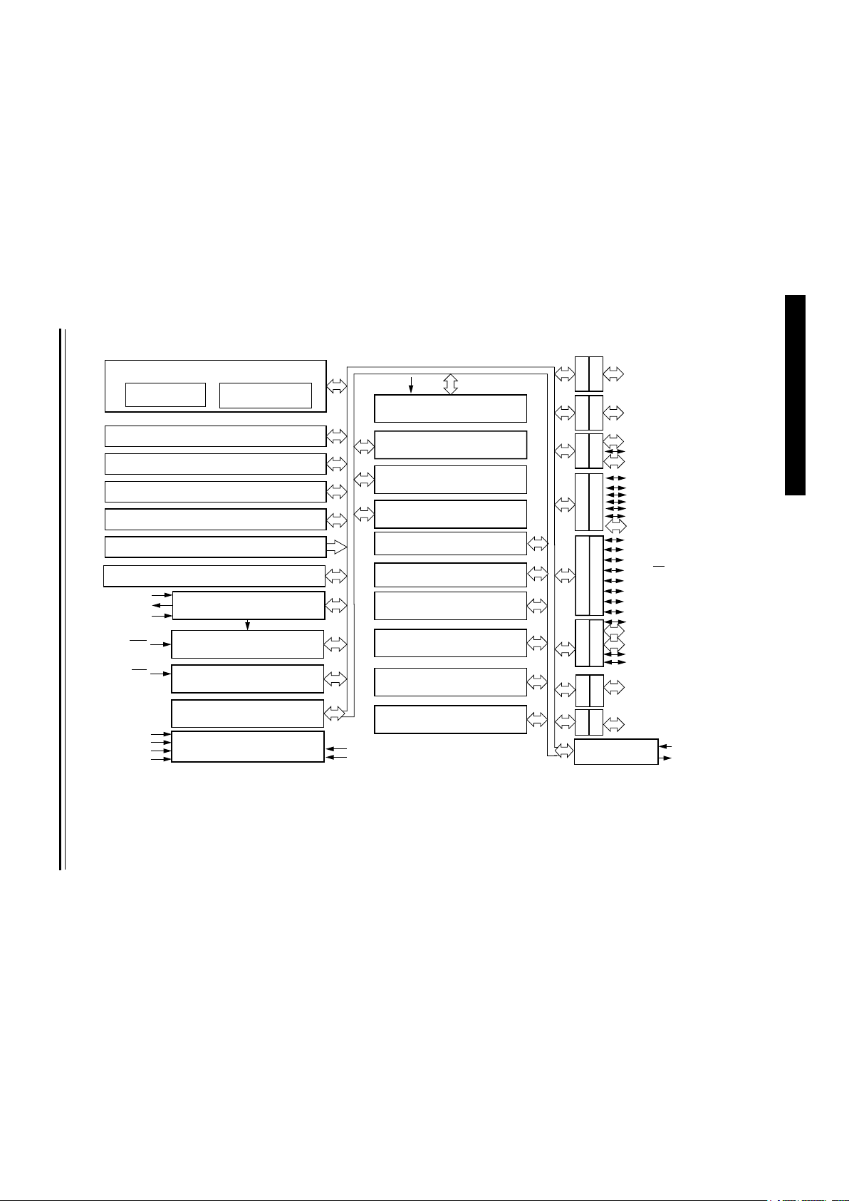
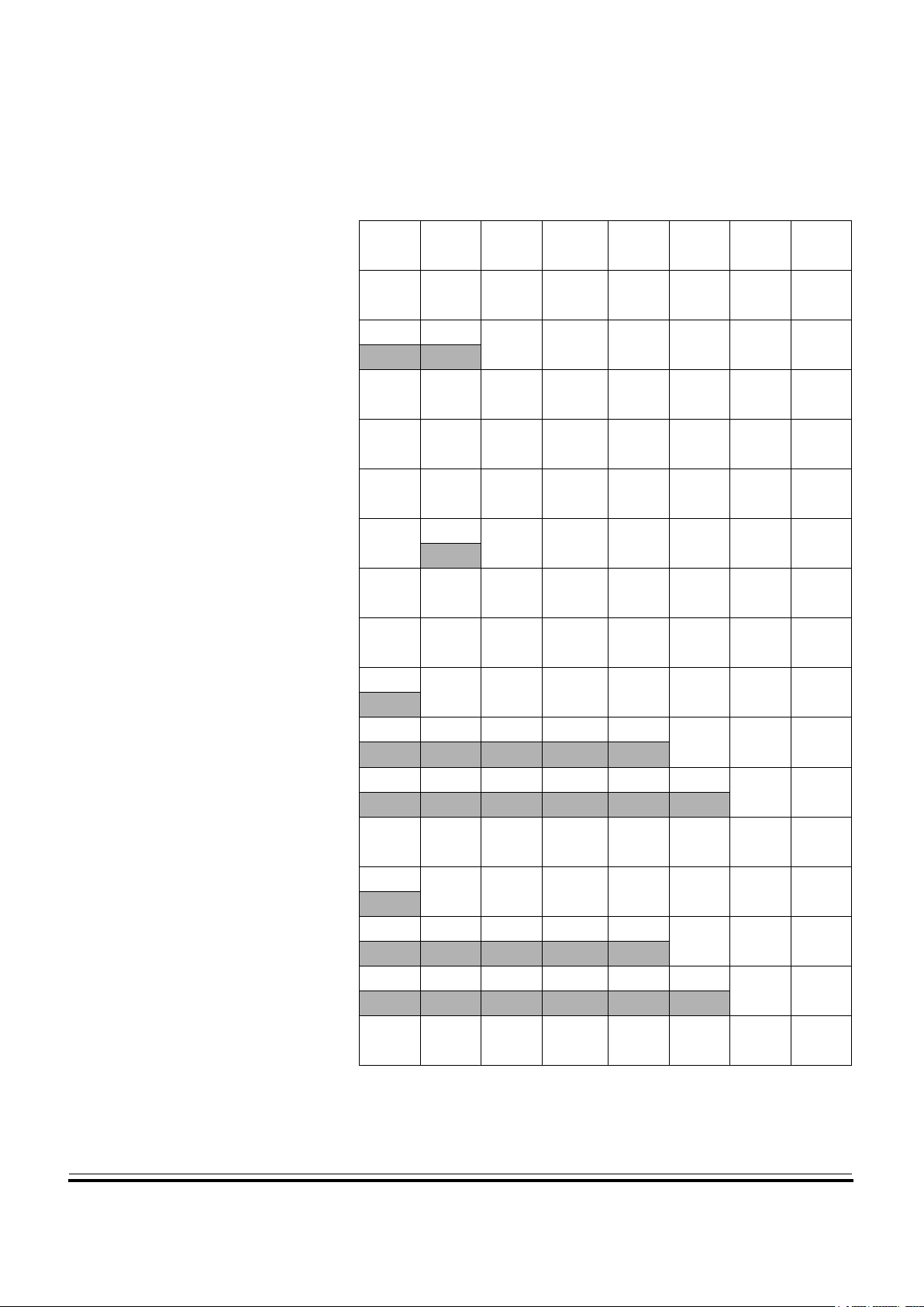
MCU Block Diagram
Figure 1 shows the structure of the MC68HC908AZ60.
3-gen
Page 16
General Description
MC68HC908AZ60 — Rev 2.0
14 General Description MOTOROLA
BREAK MODULE
CLOCK GENERATOR
MODULE
SYSTEM INTEGRATION
MODULE
ANALOG-TO-DIGITAL
MODULE
SERIAL COMMUNICATIONS
INTERFACE MODULE
SERIAL PERIPHERAL
INTERFACE MODULE
TIMER A 6 CHANNEL
INTERFACE MODULE
LOW-VOLTAGE INHIBIT
MODULE
POWER-ON RESET
MODULE
COMPUTER OPERATING
PROPERLY MODULE
ARITHMETIC/LOGIC
UNIT (ALU)
CPU
REGISTERS
M68HC08 CPU
CONTROL AND STATUS REGISTERS — 62 BYTES
USER FLASH — 60 kBYTES
USER RAM — 2048BYTES
USER EEPROM — 1024 BYTES
MONITOR ROM — 224 BYTES
IRQ MODULE
DDRD
PTD
DDRE
PTE
PTG
DDRG
OSC1
OSC2
CGMXFC
RST
IRQ
V
DD
V
DDA
V
SSA
PTE7/SPSCK
PTE6/MOSI
PTE5/MISO
PTE4/SS
PTE3/TACH1
PTE2/TACH0
PTE1/RxD
PTE0/TxD
PTF5/TBCH1–PTF4/TBCH0
PTF3/TACH5-PTF2/TACH4
PTF
DDRF
PTG2/KBD2–PTG0/KBD0
POWER
PTF1/TACH3
PTF0/TACH2
PTA
DDRA
DDRB
PTB
DDRC
PTC
PTA7–PTA0
PTB7/ATD7–PTB0/ATD0
PTC5–PTC3
PTC2/MCLK
PTC1–PTC0
V
REFH
MSCAN MODULE
TIMER B INTERFACE
MODULE
CANRx
CANTx
PTH
DDRH
PTH1/KBD4–PTH0/KBD3
KEYBOARD INTERRUPT
MODULE
V
SS
USER FLASH VECTOR SPACE — 52 BYTES
PTF6
V
DDAREF
AVSS/V
REFL
Figure 1. MCU Block Diagram for the MC68HC908AZ60 (64-Pin QFP)
PTD1/ATD9–PTD0/ATD8
PTD2/ATD10
PTD6/ATD14/TACLK
PTD5/ATD13
PTD3/ATD11
PTD4/ATD12/TBCLK
PTD7
PROGRAMMABLE INTERRUPT
TIMER (PIT) MODULE
4-gen
Page 17
General Description
Pin Assignments
MC68HC908AZ60 — Rev 2.0
MOTOROLA General Description 15
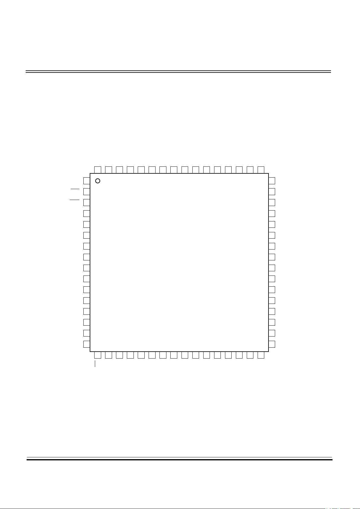
Pin Assignments
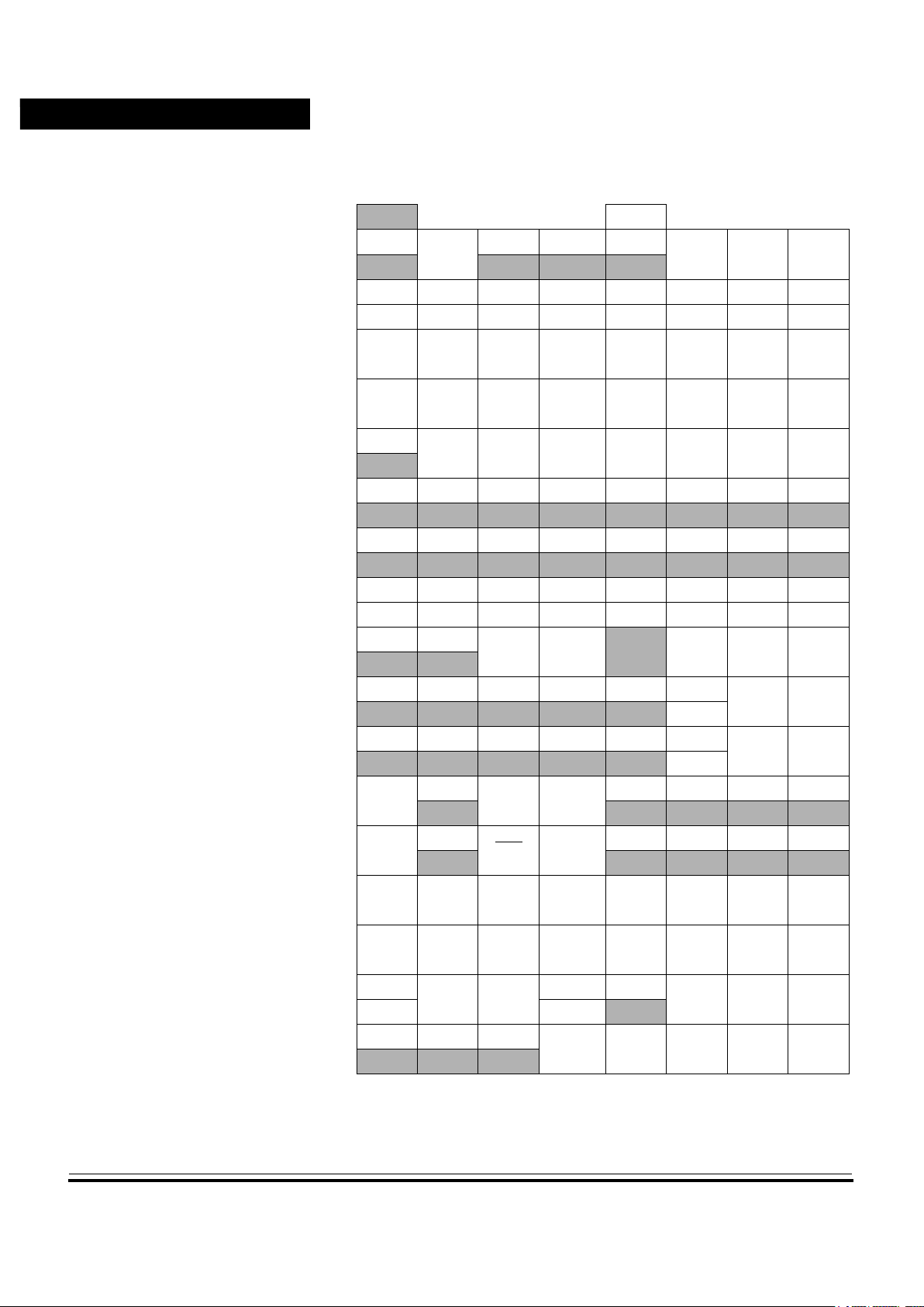
Figure 2 shows the MC68HC908AZ60 pin assignments.
Figure 2. MC68HC908AZ60 (64-Pin QFP)
NOTE:
The following pin descriptions are just a quick reference. For a more
detailed representation, see
I/O Ports
on page 305
.
PTF4/TBCH0
CGMXFC
PTB7/ATD7
PTF3/TACH5
PTF2/TACH4
PTF1/TACH3
PTF0/TACH2
RST
IRQ
PTC4
CANRx
CANTx
PTF5/TBCH1
PTE0/TxD
PTE1/RxD
PTE2/TACH0
PTE3/TACH1
PTH0/KBD3
PTD3/ATD11
PTD2/ATD10
AV
SS /VREFL
V
DDAREF
PTD1/ATD9
PTD0/ATD8
PTB6/ATD6
PTB5/ATD5
PTB4/ATD4
PTB3/ATD3
PTB2/ATD2
PTB1/ATD1
PTB0/ATD0
PTA7
V
SSAVDDA
V
REFH
PTD7
PTD6/ATD14/TACLK
PTD5/ATD13
PTD4/ATD12/TBCLK
PTH1/KBD4
PTC5
PTC3
PTC2/MCLK
PTC1
PTC0
OSC1
OSC2
PTE6/MOSI
PTE4/SS
PTE5/MISO
PTE7/SPSCK
V
SS
V
DD
PTG0/KBD0
PTG1/KBD1
PTG2/KBD2
PTA0
PTA1
PTA2
PTA3
PTA4
PTA5
PTA6
1
2
3
4
5
6
7
8
9
10
11
12
13
14
15
16
17
18
19
20
21
22
23
24
25
26
27
28
29
30
31
32
47
46
45
44
43
42
41
40
39
38
37
36
35
34
33
64
63
62
61
60
59
58
57
56
55
54
53
52
51
50
PTF6
48
49
5-gen
Page 18
General Description
MC68HC908AZ60 — Rev 2.0
16 General Description MOTOROLA
Power Supply Pins
(V
DD
and V
SS
)
V
DD
and V
SS
are the power supply and ground pins. The MCU operates
from a single power supply.
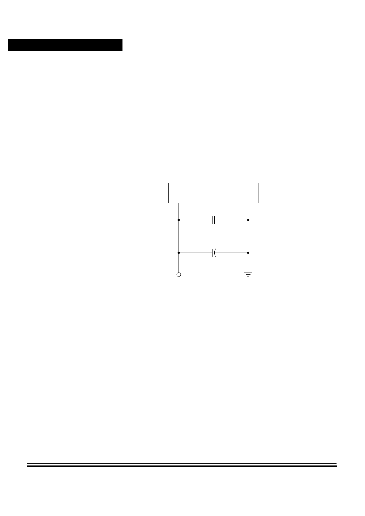
Fast signal transitions on MCU pins place high, short-duration current
demands on the power supply. To prevent noise problems, take special
care to provide power supply bypassing at the MCU as shown in Figure
3 . Place the C1 bypass capacitor as close to the MCU as possible. Use
a high-frequency response ceramic capacitor for C1. C2 is an optional
bulk current bypass capacitor for use in applications that require the port
pins to source high current levels.
V
SS
is also the ground for the port output buffers and the ground return
for the serial clock in the serial peripheral interface module (SPI). See
Serial Peripheral Interface Module (SPI) on page 237.
NOTE:
V
SS
must be grounded for proper MCU operation.
Oscillator Pins
(OSC1 and OSC2)
The OSC1 and OSC2 pins are the connections for the on-chip oscillator
circuit. See Clock Generator Module (CGM) on page 127.
Figure 3. Power supply bypassing
MCU
V
DD
C2
C1
0.1 µF
V
SS
V
DD
+
NOTE: Component values shown represent typical applications.
6-gen
Page 19

General Description
Pin Assignments
MC68HC908AZ60 — Rev 2.0
MOTOROLA General Description 17
External Reset Pin
(RST
)
A logic 0 on the RST
pin forces the MCU to a known startup state. RST
is bidirectional, allowing a reset of the entire system. It is driven low when
any internal reset source is asserted. See
System Integration Module (SIM) on page 105 for more information.
External Interrupt
Pin (IRQ
)
IRQ
is an asynchronous external interrupt pin. See
External Interrupt Module (IRQ) on page 191.
Analog Power
Supply Pin (V
DDA
)
V
DDA
is the power supply pin for the analog portion of the chip. This pin
will supply the clock generator module (CGM). See
Clock Generator Module (CGM) on page 127.
Analog Ground
Pin (V
SSA
)
The V
SSA
analog ground pin is used only for the ground connections for
the analog sections of the circuit and should be decoupled as per the
V
SS
digital ground pin. The analog sections consist of a clock generator
module (CGM). See Clock Generator Module (CGM) on page 127.
External Filter
Capacitor Pin
(CGMXFC)
CGMXFC is an external filter capacitor connection for the CGM. See
Clock Generator Module (CGM) on page 127
Port A
Input/Output (I/O)
Pins (PTA7
–
PTA0)
PTA7–PTA0 are general-purpose bidirectional I/O port pins. See I/O
Ports on page 305.
Port B I/O Pins
(PTB7/ATD7ÐPTB0/
ATD0)
Port B is an 8-bit special function port that shares all eight pins with the
analog-to-digital converter (ADC). See
Analog-to-Digital Converter (ADC-15) on page 421 and I/O Ports on
page 305.
Port C I/O Pins
(PTC5ÐPTC0)
PTC5–PTC3 and PTC1–PTC0 are general-purpose bidirectional I/O
port pins. PTC2/MCLK is a special function port that shares its pin with
7-gen
Page 20

General Description
MC68HC908AZ60 — Rev 2.0
18 General Description MOTOROLA
the system clock which has a frequency equivalent to the system clock.
See I/O Ports on page 305.
Port D I/O Pins
(PTD7ÐPTD0/ATD8)
Port D is an 8-bit special-function port that shares seven of its pins with
the analog-to-digital converter module (ADC-15), one of its pins with the
timer interface module (TIMA), and one more of its pins with the timer
interface module (TIMB). See Timer Interface Module A (TIMA-6) on
page 389, Analog-to-Digital Converter (ADC-15) on page 421 and I/O
Ports on page 305.
Port E I/O Pins
(PTE7/SPSCKÐPTE0/
TxD)
Port E is an 8-bit special function port that shares two of its pins with the
timer interface module (TIMA), four of its pins with the serial peripheral
interface module (SPI), and two of its pins with the serial communication
interface module (SCI). See
Serial Communications Interface Module (SCI) on page 199,
Serial Peripheral Interface Module (SPI) on page 237,
Timer Interface Module A (TIMA-6) on page 389, and I/O Ports on
page 305.
Port F I/O Pins
(PTF6ÐPTF0/TACH2)
Port F is a 7-bit special function port that shares its pins with the timer
interface module (TIMB). Six of its pins are shared with the timer
interface module (TIMA-6). See Timer Interface Module A (TIMA-6) on
page 389, Timer Interface Module B (TIMB) on page 269, and I/O
Ports on page 305.
Port G I/O Pins
(PTG2/KBD2ÐPTG0
/KBD0)
Port G is a 3-bit special function port that shares all of its pins with the
keyboard interrupt module (KBD). See Keyboard Module (KBD) on
page 381 and I/O Ports on page 305.
Port H I/O Pins
(PTH1/KBD4ÐPTH0/
KBD3)
Port H is a 2-bit special-function port that shares all of its pins with the
keyboard interrupt module (KBD). See Keyboard Module (KBD) on
page 381 and I/O Ports on page 305.
8-gen
Page 21

General Description
Pin Assignments
MC68HC908AZ60 — Rev 2.0
MOTOROLA General Description 19
CAN Transmit Pin
(CANTx)
This pin is the digital output from the CAN module (CANTx). See
MSCAN Controller (MSCAN08) on page 331.
CAN Receive Pin
(CANRx)
This pin is the digital input to the CAN module (CANRx). See MSCAN
Controller (MSCAN08) on page 331.
Table 1. External Pins Summary
Pin Name Function
Driver
Type
Hysteresis
(note 1)
Reset State
PTA7–PTA0 General-Purpose I/O Dual State No Input Hi-Z
PTB7/ATD7–PTB0/ATD0
General-Purpose I/O
ADC Channel
Dual State No Input Hi-Z
PTC5–PTC0 General-Purpose I/O Dual State No Input Hi-Z
PTD7 General Purpose I/O/ Dual State No Input Hi-Z
PTD6/ATD14/TACLK ADC Channel
General-Purpose I/O
ADC Channel/Timer
External Input Clock
Dual State No Input Hi-Z
PTD5/ATD13 ADC Channel General-Purpose I/O
ADC Channel
Dual State No Input Hi-Z
PTD4/ATD12/TBCLK ADC Channel
General-Purpose I/O
ADC Channel/Timer
External Input Clock
Dual State No
Input Hi-Z
PTD3/ATD11–PTD0/A TD8 ADC Channels
General-Purpose I/O
ADC Channel
Dual State
No
Input Hi-Z
PTE7/SPSCK
General-Purpose I/O
SPI Clock
Dual State
Open Drain
Yes Input Hi-Z
PTE6/MOSI
General-Purpose I/O
SPI Data Path
Dual State
Open Drain
Yes Input Hi-Z
PTE5/MISO
General-Purpose I/O
SPI Data Path
Dual State
Open Drain
Yes Input Hi-Z
PTE4/SS
General-Purpose I/O
SPI Slave Select
Dual State Yes Input Hi-Z
PTE3/TACH1
General-Purpose I/O
Timer Channel 1
Dual State Yes Input Hi-Z
PTE2/TACH0
General-Purpose I/O
Timer Channel 0
Dual State Yes Input Hi-Z
PTE1/RxD
General-Purpose I/O
SCI Receive Data
Dual State Yes Input Hi-Z
9-gen
Page 22
General Description
MC68HC908AZ60 — Rev 2.0
20 General Description MOTOROLA
PTE0/TxD
General-Purpose I/O
SCI Transmit Data
Dual State No Input Hi-Z
PTF6 General-Purpose I/O Dual State No Input Hi-Z
PTF5/TBCH1–PTF4/TBCH0
General-Purpose
I/O/Timer B Channel
Dual State Yes Input Hi-Z
PTF3/TACH5
General-Purpose I/O
Timer A Channel 5
Dual State Yes Input Hi-Z
PTF2/TACH4
General-Purpose I/O
Timer A Channel 4
Dual State Yes Input Hi-Z
PTF1/TACH3
General-Purpose I/O
Timer A Channel 3
Dual State Yes Input Hi-Z
PTF0/TACH2
General-Purpose I/O
Timer A Channel 2
Dual State Yes Input Hi-Z
PTG2/KBD2–PTG0/KBD0
General-Purpose I/O/
Keyboard W ak eup Pin
Dual State Yes Input Hi-Z
PTH1/KBD4 –PTH0/KBD3
General-Purpose I/O/
Keyboard W ak eup Pin
Dual State Yes Input Hi-Z
V
DD
Chip Power Supply N/A N/A N/A
V
SS
Chip Ground N/A N/A N/A
V
DDAREF
ADC Power Supply/
ADC Reference
Voltage
N/A N/A N/A
A
VSS/VREFL
ADC Ground/ADC
Reference V oltage
N/A N/A N/A
V
REFH
A/D Reference
Voltage
N/A N/A N/A
OSC1 External Clock In N/A N/A Input Hi-Z
OSC2 External Clock Out N/A N/A Output
CGMXFC PLL Loop Filter Cap N/A N/A N/A
IRQ
External Interrupt
Request
N/A N/A Input Hi-Z
RST Reset N/A N/A Output Low
CANRx CAN Serial Input N/A Yes Input Hi-Z
CANTx CAN Serial Output Output No Output
Table 1. External Pins Summary (Continued)
Pin Name Function
Driver
Type
Hysteresis
(note 1)
Reset State
10-gen
Page 23
General Description
Pin Assignments
MC68HC908AZ60 — Rev 2.0
MOTOROLA General Description 21
Note 1: Hysteresis is not 100% tested but is typically a minimum of
300mV
Table 2. Clock Source Summary
Module Clock Source
ADC CGMXCLK or Bus Clock
CAN CGMXCLK or CGMOUT
COP CGMXCLK
CPU Bus Clock
EEPROM RC OSC or Bus Clock
SPI Bus Clock/SPSCK
SCI CGMXCLK
TIMA-6 Bus Clock or PTD6/ATD14/TACLK
TIMB Bus Clock or PTD4/TBCLK
PIT Bus Clock
SIM CGMOUT and CGMXCLK
IRQ Bus Clock
BRK Bus Clock
LVI Bus Clock
CGM OSC1 and OSC2
11-gen
Page 24
General Description
MC68HC908AZ60 — Rev 2.0
22 General Description MOTOROLA
Ordering Information
This section contains instructions for ordering the MC68HC908AZ60.
MC Order
Numbers
Table 3. MC Order Numbers
MC Order Number
Operating
Temperature Range
MC68HC908AZ60CFU –40 °C to + 85°C
MC68HC908AZ60VFU –40
°C to + 105 °C
MC68HC908AZ60MFU –40 °C to + 125 °C
12-gen
Page 25

MC68HC908AZ60 — Rev 2.0
MOTOROLA Memory Map 23
Memory Map
Memory Map
Contents
Introduction . . . . . . . . . . . . . . . . . . . . . . . . . . . . . . . . . . . . . . . . . . . . .23
I/O Section . . . . . . . . . . . . . . . . . . . . . . . . . . . . . . . . . . . . . . . . . . . . .26
Introduction
The CPU08 can address 64 Kbytes of memory space. The memory
map, shown in Figure 1, includes:
• 60 Kbytes of FLASH EEPROM
• 2048 Bytes of RAM
• 1024 Bytes of EEPROM with Protect Option
• 52 Bytes of User-Defined Vectors
• 224 Bytes of Monitor ROM
The following definitions apply to the memory map representation of
reserved and unimplemented locations.
• Reserved — Accessing a reserved location can have
unpredictable effects on MCU operation.
• Unimplemented — Accessing an unimplemented location
causes an illegal address reset if illegal address resets are
enabled.
1-mem
Page 26

Memory Map
MC68HC908AZ60 — Rev 2.0
24 Memory Map MOTOROLA
Figure 1. Memory Map
$0000
I/O REGISTERS (64 BYTES)
$0000
↓↓
$003F $003F
$0040
I/O REGISTERS, 16 BYTES
$0040
↓↓
$004F $004F
$0050
RAM-1, 1024 BYTES
$0050
↓↓
$044F $044F
$0450
FLASH-2, 176 BYTES
$0450
↓↓
$04FF $04FF
$0500
CAN CONTROL AND MESSAGE
BUFFERS, 128 BYTES
$0500
↓↓
$057F $057F
$0580
FLASH-2, 128 BYTES
$0580
↓↓
$05FF $05FF
$0600
EEPROM-2, 512 BYTES
$0600
↓↓
$07FF $07FF
$0800
EEPROM-1, 512 BYTES
$0800
↓↓
$09FF $09FF
$0A00
RAM-2 , 1024 BYTES
$0A00
↓↓
$0DFF $0DFF
$0E00
FLASH-2, 29,184 BYTES
$0E00
↓↓
$7FFF $7FFF
$8000
FLASH-1, 32,256BYTES
$8000
↓↓
$FDFF $FDFF
$FE00 SIM BREAK STATUS REGISTER (SBSR) $FE00
$FE01 SIM RESET STATUS REGISTER (SRSR) $FE01
$FE02 RESERVED $FE02
$FE03 SIM BREAK FLAG CONTROL REGISTER (SBFCR) $FE03
2-mem
Page 27

Memory Map
Introduction
MC68HC908AZ60 — Rev 2.0
MOTOROLA Memory Map 25
$FE04 RESERVED $FE04
$FE05 RESERVED $FE05
$FE06 UNIMPLEMENTED $FE06
$FE07 RESERVED $FE07
$FE08 RESERVED $FE08
$FE09
CONFIGURA TION WRITE-ONCE REGISER
(CONFIG-2)
$FE09
$FE0A RESER VED $FE0A
$FE0B FLASH CONTROL REGISTER (FLCR1) $FE0B
$FE0C BREAK ADDRESS REGISTER HIGH (BRKH) $FE0C
$FE0D BREAK ADDRESS REGISTER LOW (BRKL) $FE0D
$FE0E BREAK STATUS AND CONTROL REGISTER (BSCR) $FE0E
$FE0F LVI STATUS REGISTER (LVISR) $FE0F
$FE10 RESERVED $FE10
$FE11 FLASH CONTROL REGISTER (FLCR2) $FE11
$FE12
UNIMPLEMENTED (5BYTES)
$FE12
↓↓
$FE17 $FE17
$FE18 EEPROM NON-VOLATILE REGISTER (EENVR2) $FE18
$FE19 EEPROM CONTROL REGISTER (EECR2) $FE19
$FE1A RESERVED $FE1A
$FE1B EEPROM ARRAY CONFIGURATION (EEACR2) $FE1B
$FE1C EEPROM NON-VOLATILE REGISTER (EENVR1) $FE1C
$FE1D EEPROM CONTROL REGISTER (EECR1) $FE1D
$FE1E RESERVED $FE1E
$FE1F EEPROM ARRAY CONFIGURATION (EEACR1) $FE1F
$FE20
MONITOR ROM (224 BYTES)
$FE20
↓↓
$FEFF $FEFF
$FF00
↓
$FF7F
UNIMPLEMENTED (128 BYTES)
$FF00
↓
$FF7F
$FF80 FLASH BLOCK PROTECT REGISTER (FLBPR1) $FF80
$FF81 FLASH BLOCK PROTECT REGISTER (FLBPR2) $FF81
$FF82
RESERVED (75 BYTES)
$FF82
↓↓
$FFCB $FFCB
Figure 1. Memory Map (Continued)
3-mem
Page 28

Memory Map
MC68HC908AZ60 — Rev 2.0
26 Memory Map MOTOROLA
I/O Section
Addresses $0000–$003F, shown in Figure 2, contain most of the
control, status, and data registers. Additional I/O registers have these
addresses:
• $FE00 (SIM break status register, SBSR)
• $FE01 (SIM reset status register, SRSR)
• $FE03 (SIM break flag control register, SBFCR)
• $FE09 (configuration write-once register, CONFIG-2)
• $FE0B (FLASH control register, FLCR1)
• $FE0C and $FE0D (break address registers, BRKH and BRKL)
• $FE0E (break status and control register, BRKSCR)
• $FE0F (LVI status register, LVISR)
• $FE11 (FLASH control register, FLCR2)
• $FE18 (EEPROM non-volatile register, EENVR2)
• $FE19 (EEPROM control register, EECR2)
• $FE1B (EEPROM array configuration register, EEACR2)
• $FE1C (EEPROM non-volatile register, EENVR1)
• $FE1D (EEPROM control register, EECR1)
• $FE1F (EEPROM array configuration register, EEACR1)
• $FF80 (FLASH block protect register, FLBPR1)
• $FF81 (FLASH block protect register, FLBPR2)
• $FFFF (COP control register, COPCTL)
Table 1 is a list of vector locations.
$FFCC
VECTORS (52BYTES)
$FFCC
↓↓
$FFFF $FFFF
Figure 1. Memory Map (Continued)
4-mem
Page 29
Memory Map
I/O Section
MC68HC908AZ60 — Rev 2.0
MOTOROLA Memory Map 27
Addr. Register Name Bit 7 6 5 4 3 2 1 Bit 0
$0000 Port A Data Register (PTA)
Read:
PTA7 PTA6 PTA5 PTA4 PTA3 PTA2 PTA1 PTA0
Write:
$0001 Port B Data Register (PTB)
Read:
PTB7 PTB6 PTB5 PTB4 PTB3 PTB2 PTB1 PTB0
Write:
$0002 Port C Data Register (PTC)
Read: 0 0
PTC5 PTC4 PTC3 PTC2 PTC1 PTC0
Write:
$0003 Port D Data Register (PTD)
Read:
PTD7 PTD6 PTD5 PTD4 PTD3 PTD2 PTD1 PTD0
Write:
$0004
Data Direction Register A
(DDRA)
Read:
DDRA7 DDRA6 DDRA5 DDRA4 DDRA3 DDRA2 DDRA1 DDRA0
Write:
$0005
Data Direction Register B
(DDRB)
Read:
DDRB7 DDRB6 DDRB5 DDRB4 DDRB3 DDRB2 DDRB1 DDRB0
Write:
$0006
Data Direction Register C
(DDRC)
Read:
MCLKEN
0
DDRC5 DDRC4 DDRC3 DDRC2 DDRC1 DDRC0
Write:
$0007
Data Direction Register D
(DDRD)
Read:
DDRD7 DDRD6 DDRD5 DDRD4 DDRD3 DDR2 DDRD1 DDRD0
Write:
$0008 Port E Data Register (PTE)
Read:
PTE7 PTE6 PTE5 PTE4 PTE3 PTE2 PTE1 PTE0
Write:
$0009 Port F Data Register (PTF)
Read: 0
PTF6 PTF5 PTF4 PTF3 PTF2 PTF1 PTF0
Write:
$000A Port G Data Register (PTG)
Read: 0 0 0 0 0
PTG2 PTG1 PTG0
Write:
$000B Port H Data Register (PTH)
Read: 0 0 0 0 0 0
PTH1 PTH0
Write:
$000C
Data Direction Register E
(DDRE)
Read:
DDRE7 DDRE6 DDRE5 DDRE4 DDRE3 DDRE2 DDRE1 DDRE0
Write:
$000D
Data Direction Register F
(DDRF)
Read: 0
DDRF6 DDRF5 DDRF4 DDRF3 DDRF2 DDRF1 DDRF0
Write:
$000E
Data Direction Register G
(DDRG)
Read: 0 0 0 0 0
DDRG2 DDRG1 DDRG0
Write:
$000F
Data Direction Register H
(DDRH)
Read: 0 0 0 0 0 0
DDRH1 DDRH0
Write:
$0010 SPI Control Register (SPCR)
Read:
SPRIE R SPMSTR CPOL CPHA SPWOM SPE SPTIE
Write:
Figure 2. Control, Status, and Data Registers (Sheet 1 of 6)
5-mem
Page 30
Memory Map
MC68HC908AZ60 — Rev 2.0
28 Memory Map MOTOROLA
= Unimplemented R = Reserved
$0011
SPI Status and Control
Register (SPSCR)
Read: SPRF
ERRIE
OVRF MODF SPTE
MODFE
N
SPR1 SPR0
Write:
$0012 SPI Data Register (SPDR)
Read: R7 R6 R5 R4 R3 R2 R1 R0
Write: T7 T6 T5 T4 T3 T2 T1 T0
$0013 SCI Control Register 1 (SCC1)
Read:
LOOPS ENSCI TXINV M WAKE ILTY PEN PTY
Write:
$0014 SCI Control Register 2 (SCC2)
Read:
SCTIE TCIE SCRIE ILIE TE RE RWU SBK
Write:
$0015 SCI Control Register 3 (SCC3)
Read: R8
T8 R R ORIE NEIE FEIE PEIE
Write:
$0016 SCI Status Register 1 (SCS1)
Read: SCTE TC SCRF IDLE OR NF FE PE
Write:
$0017 SCI Status Register 2 (SCS2)
Read: 0 0 0 0 0 0 BKF RPF
Write:
$0018 SCI Data Register (SCDR)
Read: R7 R6 R5 R4 R3 R2 R1 R0
Write: T7 T6 T5 T4 T3 T2 T1 T0
$0019 SCI Baud Rate Register (SCBR)
Read: 0 0
SCP1 SCP0 SCR2 SCR1 SCR0
Write:
$001A
IRQ Status and Control
Register (ISCR)
Read: 0 0 0 0 IRQF 0
IMASK1 MODE1
Write: ACK1
$001B
Keyboard Status and Control
Register (KBSCR)
Read: 0 0 0 0 KEYF 0
IMASKK MODEK
Write: ACKK
$001C PLL Control Register (PCTL)
Read:
PLLIE
PLLF
PLLON BCS
1111
Write:
$001D
PLL Bandwidth Control
Register (PBWC)
Read:
AUTO
LOCK
ACQ XLD
0000
Write:
$001E
PLL Programming Register
(PPG)
Read:
MUL7 MUL6 MUL5 MUL4 VRS7 VRS6 VRS5 VRS4
Write:
$001F
Configuration Write-Once
Register (CONFIG-1)
Read:
LVISTOP R LVIRST LVIPWR SSREC COPL STOP COPD
Write:
$0020
Timer A Status and Control
Register (TASC)
Read: TOF
TOIE TSTOP
00
PS2 PS1 PS0
Write: 0 TRST
$0021
Keyboard Interrupt Enable Register
(KBIE)
Read: 0 0 0
KBIE4 KBIE3 KBIE2 KBIE1 KBIE0
Write:
Addr. Register Name Bit 7 6 5 4 3 2 1 Bit 0
Figure 2. Control, Status, and Data Registers (Sheet 2 of 6)
6-mem
Page 31

Memory Map
I/O Section
MC68HC908AZ60 — Rev 2.0
MOTOROLA Memory Map 29
$0022
Timer A Counter Register
High (TACNTH)
Read: Bit 15 14 13 12 11 10 9 Bit 8
Write:
$0023
Timer A Counter Register
Low (TACNTL)
Read: Bit 7 6 5 4 3 2 1 Bit 0
Write:
$0024
Timer A Modulo Register
High (TAMODH)
Read:
Bit 15 14 13 12 11 10 9 Bit 8
Write:
$0025
Timer A Modulo Register
Low (TAMODL)
Read:
Bit 7 6 5 4 3 2 1 Bit 0
Write:
$0026
Timer A Channel 0 Status and
Control Register (TASC0)
Read: CH0F
CH0IE MS0B MS0A ELS0B ELS0A TOV0 CH0MAX
Write: 0
$0027
Timer A Channel 0 Register
High (TACH0H)
Read:
Bit 15 14 13 12 11 10 9 Bit 8
Write:
$0028
Timer A Channel 0 Register
Low (TACH0L)
Read:
Bit 7 6 5 4 3 2 1 Bit 0
Write:
$0029
Timer A Channel 1 Status and
Control Register (TASC1)
Read: CH1F
CH1IE
0
MS1A ELS1B ELS1A TOV1 CH1MAX
Write: 0
$002A
Timer A Channel 1 Register
High (TACH1H)
Read:
Bit 15 14 13 12 11 10 9 Bit 8
Write:
$002B
Timer A Channel 1 Register
Low (TACH1L)
Read:
Bit 7 6 5 4 3 2 1 Bit 0
Write:
$002C
Timer A Channel 2 Status and
Control Register (TASC2)
Read: CH2F
CH2IE MS2B MS2A ELS2B ELS2A TOV2 CH2MAX
Write: 0
$002D
Timer A Channel 2 Register
High (TACH2H)
Read:
Bit 15 14 13 12 11 10 9 Bit 8
Write:
$002E
Timer A Channel 2 Register
Low (TACH2L)
Read:
Bit 7 6 5 4 3 2 1 Bit 0
Write:
$002F
Timer A Channel 3 Status and
Control Register (TASC3)
Read: CH3F
CH3IE
0
MS3A ELS3B ELS3A TOV3 CH3MAX
Write: 0
$0030
Timer A Channel 3 Register
High (TACH3H)
Read:
Bit 15 14 13 12 11 10 9 Bit 8
Write:
$0031
Timer A Channel 3 Register
Low (TACH3L)
Read:
Bit 7 6 5 4 3 2 1 Bit 0
Write:
$0032
Timer A Channel 4 Status and
Control Register (TASC4)
Read: CH4F
CH4IE MS4B MS4A ELS4B ELS4A TOV4 CH4MAX
Write: 0
$0033
Timer A Channel 4 Register High
(TACH4H)
Read:
Bit 15 14 13 12 11 10 9 Bit 8
Write:
Addr. Register Name Bit 7 6 5 4 3 2 1 Bit 0
Figure 2. Control, Status, and Data Registers (Sheet 3 of 6)
7-mem
Page 32

Memory Map
MC68HC908AZ60 — Rev 2.0
30 Memory Map MOTOROLA
$0034
Timer A Channel 4 Register Low
(TACH4L)
Read:
Bit 7 6 5 4 3 2 1 Bit 0
Write:
$0035
Timer A Channel 5 Status and
Control Register (TASC5)
Read: CH5F
CH5IE
0
MS5A ELS5B ELS5A TOV5 CH5MAX
Write: 0
$0036
Timer A Channel 5 Register
High (TACH5H)
Read:
Bit 15 14 13 12 11 10 9 Bit 8
Write:
$0037
Timer A Channel 5 Register
Low (TACH5L)
Read:
Bit 7 6 5 4 3 2 1 Bit 0
Write:
$0038
Analog-to-Digital Status and
Control Register (ADSCR)
Read:
COCO AIEN ADCO ADCH4 ADCH3 ADCH2 ADCH1 ADCH0
Write:
$0039
Analog-to-Digital Data Register
(ADR)
Read: AD7 AD6 AD5 AD4 AD3 AD2 AD1 AD0
Write:
$003A
Analog-to-Digital Input Clock
Register (ADICLK)
Read:
ADIV2 ADIV1 ADIV0 ADICLK
0000
Write:
$0040
Timer B Status and Control
Register (TBSCR)
Read: TOF
TOIE TSTOP
00
PS2 PS1 PS0
Write: TRST
$0041
Timer B Counter Register High
(TBCNTH)
Read: Bit 15 14 13 12 11 10 9 Bit 8
Write:
$0042
Timer B Counter Register Low
(TBCNTL)
Read: Bit 7 6 5 4 3 2 1 Bit 0
Write:
$0043
Timer B Modulo Register High
(TBMODH)
Read:
Bit 15 14 13 12 11 10 9 Bit 8
Write:
$0044
Timer B Modulo Register Low
(TBMODL)
Read:
Bit 7 6 5 4 3 2 1 Bit 0
Write:
$0045
Timer B CH0 Status and Control
Register (TBSC0)
Read: CH0F
CH0IE MS0B MS0A ELS0B ELS0A TOV0 CH0MAX
Write: 0
$0046
Timer B CH0 Register High
(TBCH0H)
Read:
Bit 15 14 13 12 11 10 9 Bit 8
Write:
$0047
Timer B CH0 Register Low
(TBCH0L)
Read:
Bit 7 6 5 4 3 2 1 Bit 0
Write:
Timer B CH1 Status and Control
Register (TBSC1)
Read: CH1F
CH1IE
0
MS1A ELS1B ELS1A TOV1 CH1MAX
$0048 Write: 0
$0049
Timer B CH1 Register High
(TBCH1H)
Read:
Bit 15 14 13 12 11 10 9 Bit 8
Write:
$004A
Timer B CH1 Register Low
(TBCH1L)
Read:
Bit 7 6 5 4 3 2 1 Bit 0
Write:
Addr. Register Name Bit 7 6 5 4 3 2 1 Bit 0
Figure 2. Control, Status, and Data Registers (Sheet 4 of 6)
8-mem
Page 33

Memory Map
I/O Section
MC68HC908AZ60 — Rev 2.0
MOTOROLA Memory Map 31
$004B
PIT Status and Control Register
(PSC)
Read: POF
PIE PSTOP
00
PPS2 PPS1 PPS0
Write: PRST
$004C
PIT Counter Register High
(PCNTH)
Read: Bit 15 14 13 12 11 10 9 Bit 8
Write:
$004D PIT Counter Register Low (PCNTL)
Read: Bit 7 6 5 4 3 2 1 Bit 0
Write:
$004E
PIT Modulo Register High
(PMODH)
Read:
Bit 15 14 13 12 11 10 9 Bit 8
Write:
$004F PIT Modulo Register Low (PMODL)
Read:
Bit 7 6 5 4 3 2 1 Bit 0
Write:
$FE00
SIM Break Status Register
(SBSR)
Read:
R R R R R RBWR
Write:
$FE01 SIM Reset Status Register (SRSR)
Read: POR PIN COP ILOP ILAD 0 LVI 0
Write:
$FE03
SIM Break Flag Control Register
(SBFCR)
Read:
BCFE R R R R R R R
Write:
$FE09
Configuration Write-Once Register
(CONFIG-2)
Read:
0 0 0 MSCAND 0 0 0 AZxx
Write:
$FE0B
Flash Control Register
(FLCR1)
Read:
FDIV1 FDIV0 BLK1 BLK0 HVEN VERF ERASE PGM
Write:
$FE0C
Break Address Register High
(BRKH)
Read:
Bit 15 14 13 12 11 10 9 Bit 8
Write:
$FE0D
Break Address Register Low
(BRKL)
Read:
Bit 7 6 5 4 3 2 1 Bit 0
Write:
$FE0E
Break Status and Control
Register (BRKSCR)
Read:
BRKE BRKA
000000
Write:
$FE0F LVI Status Register (LVISR)
Read: LVIOUT 0 0 0 0 0 0 0
Write:
$FE11
Flash Control Register
(FLCR2)
Read:
FDIV1 FDIV0 BLK1 BLK0 HVEN VERF ERASE PGM
Write:
$FE18
EEPROM Nonvolatile Register
(EENVR2)
Read:
EERA CON2 CON1 EEPRTCT EEBP3 EEBP2 EEBP1 EEBP0
Write:
$FE19
EEPROM Control
Register (EECR2)
Read:
EEBCLK
0
EEOFF EERAS1 EERAS0 EELAT
0
EEPGM
Write:
$FE1A Reserved
Read:
RRRR RRRR
Write:
Addr. Register Name Bit 7 6 5 4 3 2 1 Bit 0
Figure 2. Control, Status, and Data Registers (Sheet 5 of 6)
9-mem
Page 34

Memory Map
MC68HC908AZ60 — Rev 2.0
32 Memory Map MOTOROLA
$FE1B
EEPROM Array Control Register
(EEACR2)
Read: EERA CON2 CON1 EEPRTCT EEBP3 EEBP2 EEBP1 EEBP0
Write:
$FE1C
EEPROM Nonvolatile Register
(EENVR1)
Read:
EERA CON2 CON1 EEPRTCT EEBP3 EEBP2 EEBP1 EEBP0
Write:
$FE1D
EEPROM Control
Register (EECR1)
Read:
EEBCLK
0
EEOFF EERAS1 EERAS0 EELAT
0
EEPGM
Write:
$FE1E Reserved
Read:
RRRR RRRR
Write:
$FE1F
EEPROM Array Control Register
(EEACR1)
Read: EERA CON2 CON1 EEPRTCT EEBP3 EEBP2 EEBP1 EEBP0
Write:
$FF80
FLASH Block Protect Register
(FLBPR1)
Read: BPR3 BPR2 BPR1 BPR0
Write:
$FF81
FLASH Block Protect Register
(FLBPR2)
Read: BPR3 BPR2 BPR1 BPR0
Write:
$FFFF COP Control Register (COPCTL)
Read: LOW BYTE OF RESET VECTOR
Write: WRITING TO $FFFF CLEARS COP COUNTER
Addr. Register Name Bit 7 6 5 4 3 2 1 Bit 0
Figure 2. Control, Status, and Data Registers (Sheet 6 of 6)
10-mem
Page 35

Memory Map
I/O Section
MC68HC908AZ60 — Rev 2.0
MOTOROLA Memory Map 33
Table 1. Vector Addresses
Address Vector
Low
$FFCC TIMA Channel 5 Vector (High)
$FFCD TIMA Channel 5 Vector (Low)
$FFCE TIMA Channel 4 Vector (High)
$FFCF TIMA Channel 4 Vector (Low)
$FFD0 ADC V ector (High)
$FFD1 ADC V ector (Low)
$FFD2 Keyboard Vector (High)
$FFD3 Keyboard Vector (Low)
$FFD4 SCI T r ansmit V ector (High)
$FFD5 SCI T r ansmit V ector (Low)
$FFD6 SCI Receive Vector (High)
$FFD7 SCI Receive Vector (Low)
$FFD8 SCI Error Vector (High)
$FFD9 SCI Error Vector (Low)
$FFDA CAN T ransmit V ector (High)
$FFDB CAN Transmit V ector (Low)
$FFDC CAN Receive Vector (High)
$FFDD CAN Receive Vector (Low)
$FFDE CAN Error Vector (High)
$FFDF CAN Error Vector (Low)
$FFE0 CAN Wakeup Vector (High)
$FFE1 CAN Wakeup Vector (Low)
$FFE2 SPI T ransmit Vector (High)
$FFE3 SPI T ransmit Vector (Low)
$FFE4 SPI Receive Vector (High)
$FFE5 SPI Receive Vector (Low)
$FFE6 TIMB Overflow Vector (High)
$FFE7 TIMB Overflow Vector (Low)
$FFE8 TIMB CH1 Vector (High)
$FFE9 TIMB CH1 Vector (Low)
$FFEA TIMB CH0 Vector (High)
$FFEB TIMB CH0 Vector (Low)
$FFEC TIMA Overflow Vector (High)
$FFED TIMA Overflow Vector (Low)
$FFEE TIMA CH3 Vector (High)
$FFEF TIMA CH3 Vector (Low)
Priority
11-mem
Page 36

Memory Map
MC68HC908AZ60 — Rev 2.0
34 Memory Map MOTOROLA
$FFF0 TIMA CH2 Vector (High)
$FFF1 TIMA CH2 Vector (Low)
$FFF2 TIMA CH1 Vector (High)
$FFF3 TIMA CH1 Vector (Low)
$FFF4 TIMA CH0 Vector (High)
$FFF5 TIMA CH0 Vector (Low)
$FFF6 PIT Vector (High)
$FFF7 PIT Vector (Low)
$FFF8 PLL Vector (High)
$FFF9 PLL Vector (Low)
$FFF A IRQ1 Vector (High)
$FFFB IRQ1 V ector (Low)
$FFFC SWI V ector (High)
$FFFD SWI V ector (Low)
High
$FFFE Reset V ector (High)
$FFFF Reset Vector (Low)
It is recommended that all vector addresses are defined.
Table 1. Vector Addresses (Continued)
Address Vector
Priority
12-mem
Page 37

MC68HC908AZ60 — Rev 2.0
MOTOROLA RAM 35
RAM
RAM
Contents
Introduction . . . . . . . . . . . . . . . . . . . . . . . . . . . . . . . . . . . . . . . . . . . . .35
Functional Description. . . . . . . . . . . . . . . . . . . . . . . . . . . . . . . . . . . . . 35
Introduction
This section describes the 2048 bytes of random-access memory
(RAM).
Functional Description
Addresses $0050 through $044F and $0A00 through $0DFF are RAM
locations. The location of the stack RAM is programmable with the reset
stack pointer instruction (RSP). The 16-bit stack pointer allows the stack
RAM to be anywhere in the 64K-byte memory space.
NOTE:
For correct operation, the stack pointer must point only to RAM
locations.
Within page zero are 176 bytes of RAM. Because the location of the
stack RAM is programmable, all page zero RAM locations can be used
for input/output (I/O) control and user data or code. When the stack
pointer is moved from its reset location at $00FF, direct addressing
mode instructions can access all page zero RAM locations efficiently.
Page zero RAM, therefore, provides ideal locations for frequently
accessed global variables.
Before processing an interrupt, the CPU uses five bytes of the stack to
save the contents of the CPU registers.
1-ram
Page 38

RAM
MC68HC908AZ60 — Rev 2.0
36 RAM MOTOROLA
NOTE:
For M68HC05, M6805, and M146805 compatibility, the H register is not
stacked.
During a subroutine call, the CPU uses two bytes of the stack to store
the return address. The stack pointer decrements during pushes and
increments during pulls.
NOTE:
Be careful when using nested subroutines. The CPU could overwrite
data in the RAM during a subroutine or during the interrupt stacking
operation.
2-ram
Page 39

MC68HC908AZ60 — Rev 2.0
MOTOROLA FLASH-1 Memory 37
FLASH-1 Memory
FLASH-1 Memory
Contents
Introduction . . . . . . . . . . . . . . . . . . . . . . . . . . . . . . . . . . . . . . . . . . . . .37
Future FLASH Memory. . . . . . . . . . . . . . . . . . . . . . . . . . . . . . . . . . . .37
Functional Description. . . . . . . . . . . . . . . . . . . . . . . . . . . . . . . . . . . . . 38
FLASH-1 Control Register . . . . . . . . . . . . . . . . . . . . . . . . . . . . . . . . .39
FLASH Charge Pump Frequency Control. . . . . . . . . . . . . . . . . . . . . .41
FLASH Erase Operation . . . . . . . . . . . . . . . . . . . . . . . . . . . . . . . . . . .41
FLASH Program/Margin Read Operation . . . . . . . . . . . . . . . . . . . . . .43
Smart Programming Algorithm . . . . . . . . . . . . . . . . . . . . . . . . . . . .45
FLASH Block Protection . . . . . . . . . . . . . . . . . . . . . . . . . . . . . . . . . . . 46
FLASH-1 Block Protect Register. . . . . . . . . . . . . . . . . . . . . . . . . . . . .47
FLASH-2 Block Protect Register. . . . . . . . . . . . . . . . . . . . . . . . . . . . .48
Low-Power Modes . . . . . . . . . . . . . . . . . . . . . . . . . . . . . . . . . . . . . . .50
WAIT Mode. . . . . . . . . . . . . . . . . . . . . . . . . . . . . . . . . . . . . . . . . . .50
STOP Mode . . . . . . . . . . . . . . . . . . . . . . . . . . . . . . . . . . . . . . . . . .50
Introduction
This section describes the operation of the embedded FLASH-1
memory. This memory can be read, programmed, and erased from a
single external supply. The program and erase operations are enabled
through the use of an internal charge pump.
Future FLASH Memory
Design is underway to introduce an improved Flash memory module.
The new module will offer improved write erase cycling and faster
programming times. However Flash program and erase algorithms will
3-flash-1
Page 40

FLASH-1 Memory
MC68HC908AZ60 — Rev 2.0
38 FLASH-1 Memory MOTOROLA
change, as will the block protection. The new silicon can be identified by
an ‘A’ suffix, i.e. 68HC908AZ60A, and by mask set.
NOTE:
In order that current software is compatible and also to prevent problems
if code should runaway, Flash program and erase algorithms should not
be embedded in software.
Functional Description
The FLASH memory physically consists of two independent arrays of 32K
bytes with an additional 52 bytes of user vectors and two bytes of block
protection. An erased bit reads as a logic 0 and a programmed bit reads
as a logic 1. Program and erase operations are facilitated through control
bits in a memory mapped register. Details for these operations appear
later in this section. Memory in the FLASH array is organized into pages
within rows. There are 8 pages of memory per row with 8 bytes per page.
The minimum erase block size is a single row, 64 bytes. Programming is
performed on a per page basis; eight bytes at a time. The address ranges
for the user memory, control register and vectors are:
• $8000–$FDFF
• $FF80–FF81 (Block Protect Registers)
• $FE0B FLASH Control Register
• $FFCC–$FFFF (These locations are reserved for user-defined
interrupt and reset vectors.)
When programming the FLASH, just enough program time must be used
to program a page. Too much program time can result in a program
disturb condition; in which case an erased bit on the row being
programmed becomes unintentionally programmed. Program disturb is
avoided by using an iterative program and margin read technique known
as the smart programming algorithm. The smart programming algorithm
is required whenever programming the FLASH (See FLASH
Program/Margin Read Operation on page 43). As well, to avoid the
program disturb issue, each storage page of the row should not be
programmed more than once before it is erased. The 8 program cycle
maximum per row aligns with the architecture’s 8 pages of storage per
4-flash-1
Page 41

FLASH-1 Memory
FLASH-1 Control Register
MC68HC908AZ60 — Rev 2.0
MOTOROLA FLASH-1 Memory 39
5-flash-1
row. The margin read step of the smart programming algorithm is used
to insure programmed bits are programmed to sufficient margin for data
retention over the device lifetime. The following is the row architecture
for this array:
• $8000–$803F (Row0)
• $8040–$807F (Row1)
• $8080–$80BF (Row2)
• ----------------------------
• $FFC0–$FFFF(Row 511)
Programming tools are available from Motorola. Contact your local
Motorola representative for more information.
NOTE:
A security feature prevents viewing of the FLASH contents.
1
FLASH-1 Control Register
The FLASH-1 control register controls FLASH-1 program, erase, and
margin read operations.
FDIV1 — Frequency Divide Control Bit
This read/write bit together with FDIV0 selects the factor by which the
charge pump clock is divided from the system clock. See FLASH
Charge Pump Frequency Control on page 41.
1. No security feature is absolutely secure. However, Motorola’s strategy is to make reading or
copying the FLASH difficult for unauthorized users.
Address: $FE0B
Bit 7 654321Bit 0
Read:
FDIV1 FDIV0 BLK1 BLK0 HVEN MARGIN ERASE PGM
Write:
Reset: 00000000
Figure 1. FLASH-1 Control Register (FLCR1)
Page 42

FLASH-1 Memory
MC68HC908AZ60 — Rev 2.0
40 FLASH-1 Memory MOTOROLA
FDIV0 — Frequency Divide Control Bit
This read/write bit together with FDIV1 selects the factor by which the
charge pump clock is divided from the system clock. See FLASH
Charge Pump Frequency Control on page 41.
BLK1— Block Erase Control Bit
This read/write bit together with BLK0 allows erasing of blocks of
varying size. See FLASH Erase Operation on page 41 for a
description of available block sizes.
BLK0 — Block Erase Control Bit
This read/write bit together with BLK1 allows erasing of blocks of
varying size. See FLASH Erase Operation on page 41 for a
description of available block sizes.
HVEN — High-Voltage Enable Bit
This read/write bit enables the charge pump to drive high voltages for
program and erase operations in the array. HVEN can only be set if
either PGM = 1 or ERASE = 1 and the proper sequence for
program/margin read or erase is followed.
1 = High voltage enabled to array and charge pump on
0 = High voltage disabled to array and charge pump off
MARGIN — Margin Read Control Bit
This read/write bit configures the memory for margin read operation.
MARGIN cannot be set if the HVEN = 1. MARGIN will automatically
return to unset (0) if asserted when HVEN = 1.
1 = Margin read operation selected
0 = Margin read operation unselected
ERASE — Erase Control Bit
This read/write bit configures the memory for erase operation.
ERASE is interlocked with the PGM bit such that both bits cannot be
set at the same time.
1 = Erase operation selected
0 = Erase operation unselected
6-flash-1
Page 43

FLASH-1 Memory
FLASH Charge Pump Frequency Control
MC68HC908AZ60 — Rev 2.0
MOTOROLA FLASH-1 Memory 41
7-flash-1
PGM — Program Control Bit
This read/write bit configures the memory for program operation.
PGM is interlocked with the ERASE bit such that both bits cannot be
set at the same time.
1 = Program operation selected
0 = Program operation unselected
FLASH Charge Pump Frequency Control
The internal charge pump, required for program, margin read, and erase
operations, is designed to operate most efficiently with a 2MHz clock.
The charge pump clock is derived from the bus clock. Table 1 shows
how the FDIV bits are used to select a charge pump frequency based on
the bus clock frequency. Program, margin read and erase operations
cannot be performed if the bus clock frequency is below 2 MHz.
NOTE:
FDIV0 and FDIV1 must be set to the same value in both flash arrays.
FLASH Erase Operation
Memory Characteristics on page 445 has a detailed description of the
times used in this algorithm. Use the following procedure to erase a
block of FLASH memory:
1. Set the ERASE bit, the BLK0, BLK1, FDIV0, and FDIV1 bits in the
FLASH-1 control register. See Table 2 for block sizes. See Table
1 for FDIV settings.
Table 1. Charge Pump Clock Frequency
FDIV1 FDIV0 Pump Clock Frequency Bus Clock Frequency
0 0 Bus Frequency ÷ 1 2 MHz ± 10%
0 1 Bus Frequency ÷ 2 4 MHz ± 10%
1 0 Bus Frequency ÷ 2 4 MHz ± 10%
1 1 Bus Frequency ÷ 4 8 MHz ± 10%
Page 44

FLASH-1 Memory
MC68HC908AZ60 — Rev 2.0
42 FLASH-1 Memory MOTOROLA
2. Insure target portion of array is unprotected, read the block protect
register: address $FF80. See FLASH Block Protection on page 46
and FLASH-1 Block Protect Register on page 47 for more
information.
3. Write to any FLASH address with any data within the block
address range desired.
4. Set the HVEN bit.
5. Wait for a time, t
ERASE
.
6. Clear the HVEN bit.
7. Wait for a time, t
KILL
, for the high voltages to dissipate.
8. Clear the ERASE bit.
9. After time t
HVD
, the memory can be accessed in read mode again.
NOTE:
While these operations must be performed in the order shown, other
unrelated operations may occur between the steps.
Table 2 shows the various block sizes which can be erased in one erase
operation.
In step 2 of the erase operation, the cared addresses are latched and
used to determine the location of the block to be erased. For instance,
with BLK0 = BLK1 = 0, writing to any Flash address in the range $8000
to $FFFF will enable the full-array erase.
Table 2. Erase Block Sizes
BLK1 BLK0 Block Size, Addresses Cared
0 0 Full Array: 24 Kbytes
0 1 One-Half Array: 16 Kbytes (A14 )
1 0 Eight Rows: 512 Bytes (A14–A9)
1 1 Single Row: 64 Bytes (A14–A6)
8-flash-1
Page 45

FLASH-1 Memory
FLASH Program/Margin Read Operation
MC68HC908AZ60 — Rev 2.0
MOTOROLA FLASH-1 Memory 43
9-flash-1
FLASH Program/Margin Read Operation
NOTE:
After a total of 8 program operations have been applied to a row, the row
must be erased before further programming in order to avoid program
disturb. An erased byte will read $00.
Programming of the FLASH memory is done on a page basis. A page
consists of eight consecutive bytes starting from address $XXX0 or
$XXX8. The purpose of the margin read mode is to ensure that data has
been programmed with sufficient margin for long-term data retention.
While performing a margin read the operation is the same as for ordinary
read mode except that a built-in counter stretches the data access for an
additional eight cycles to allow sensing of the lower cell current. Margin
read mode imposes a more stringent read condition on the bitcell to
insure the bitcell is programmed with enough margin for long-term data
retention. During these eight cycles the COP counter continues to run.
The user must account for these extra cycles within COP feed loops. A
margin read cycle can only follow a page programming operation. To
program and margin read the FLASH memory, use the following
algorithm. Memory Characteristics on page 445, has a detailed
description of the times used in this algorithm.
1. Set the PGM bit. This configures the memory for program
operation and enables the latching of address and data for
programming.
2. Read from the block protect register.
3. Write data to the eight bytes of the page being programmed. This
requires eight separate write operations.
4. Set the HVEN bit.
5. Wait for time, t
PROG
.
6. Clear the HVEN bit.
7. Wait for time, t
HVTV
.
8. Set the MARGIN bit.
9. Wait for time, t
VTP
.
10. Clear the PGM bit.
11. Wait for time, t
HVD
.
Page 46

FLASH-1 Memory
MC68HC908AZ60 — Rev 2.0
44 FLASH-1 Memory MOTOROLA
12. Read back data in margin read mode. This is done in eight
separate read operations which are each stretched by eight
cycles.
13. Clear the MARGIN bit.
NOTE:
While these operations must be performed in the order shown, other
unrelated operations may occur between the steps. It is highly
recommended that the interrupt mask is set during programming. Under
very controlled situations it may be possible to omit this step, but it
remains the user’s responsibility to ensure that any interrupts do not
interfere with the Flash being programmed properly.
This program/margin read sequence is repeated throughout the memory
until all data is programmed. The Smart Programming Algorithm is
always required when programming any part of the array. This algorithm
insures the minimum possible program time and avoids the deleterious
program disturb effect. (See FLASH Erase Operation on page 41).
NOTE:
In order to ensure proper FLASH read operation after completion of the
smart programming algorithm, a series of 500 dummy FLASH reads
must be performed of any address before accurate data is read from the
FLASH.
10-flash-1
Page 47

FLASH-1 Memory
FLASH Program/Margin Read Operation
MC68HC908AZ60 — Rev 2.0
MOTOROLA FLASH-1 Memory 45
11-flash-1
Smart
Programming
Algorithm
Program FLASH 2TS
Initialize Attempt Counter
Set PGM Bit and FDIV bits
Wait t
HVTV
Wait t
VTP
Set HVEN Bit
Clear PGM Bit
Set MARGIN Bit
Wait t
HVD
Increment Attempt Counter
Y
N
to Zero
Y
N
Programming Operation
Failed
Programming Operation
Complete
Write Data to
Selected Page
Wait t
STEP
Clear HVEN Bit
Margin Read Page of Data
Clear MARGIN Bit
Margin Read Data
Equal To
Write Data?
Attempt Count
Equal To
fls
PULSES
?
Read Flash Block Protect Register
Page Program/Margin Read Procedure
Note: This page program algorithm
assumes the page/s to be programmed
are initially erased.
Note: This algorithm is mandatory for
programming the FLASH 2TS.
Set Interrupt Mask: SEI Instruction
Clear MARGIN Bit
Clear Interrupt Mask: CLI Instr.
(see note above)
(see note above)
Page 48

FLASH-1 Memory
MC68HC908AZ60 — Rev 2.0
46 FLASH-1 Memory MOTOROLA
FLASH Block Protection
NOTE:
In performing a program or erase operation the FLASH Block Protect
Register must be read after setting the PGM or ERASE bit and before
asserting the HVEN bit.
Due to the ability of the on-board charge pump to erase and program the
FLASH memory in the target application, provision is made for protecting
blocks of memory from unintentional erase or program operations due to
system malfunction. This protection is done by reserving a location in the
memory for block protect information and requiring that this location be
read from to enable setting of the HVEN bit. When the block protect
register is read, its contents are latched by the FLASH control logic. If
the address range for an erase or program operation includes a
protected block, the PGM or ERASE bit is cleared which prevents the
HVEN bit in the FLASH control register from being set so that no high
voltage is allowed in the array.
When the block protect register is erased (all 0s), the entire memory is
accessible for program and erase. When bits within the register are
programmed, they lock blocks of memory address ranges as shown in
FLASH-1 Block Protect Register on page 47. The block protect register
itself can be erased or programmed only with an external voltage V
HI
present on the IRQ
pin. The presence of VHI on the IRQ pin also allows
entry in to monitor mode out of reset. Therefore, the ability to change the
block protect register is voltage dependent and can occur in either user
or monitor modes.
12-flash-1
Page 49

FLASH-1 Memory
FLASH-1 Block Protect Register
MC68HC908AZ60 — Rev 2.0
MOTOROLA FLASH-1 Memory 47
13-flash-1
FLASH-1 Block Protect Register
The block protect register is implemented as a byte within the FLASH-1
memory. Each bit, when programmed, protects a range of addresses in
the FLASH-1 array.
BPR3 — Block Protect Register Bit 3
This bit protects the memory contents in the address range $C000 to
$FFFF.
1 = Address range protected from erase or program
0 = Address range open to erase or program
BPR2 — Block Protect Register Bit 2
This bit protects the memory contents in the address range $A000 to
$FFFF.
1 = Address range protected from erase or program
0 = Address range open to erase or program
BPR1 — Block Protect Register Bit 1
This bit protects the memory contents in the address range $9000 to
$FFFF.
1 = Address range protected from erase or program
0 = Address range open to erase or program
Address: $FF80
Bit 7 654321Bit 0
Read: 0000
BPR3 BPR2 BPR1 BPR0
Write:
Reset: 00000000
= Unimplemented
Figure 2. FLASH-1 Block Protect Register (FLBPR1)
Page 50

FLASH-1 Memory
MC68HC908AZ60 — Rev 2.0
48 FLASH-1 Memory MOTOROLA
BPR0 — Block Protect Register Bit 0
This bit protects the memory contents in the address range $8000 to
$FFFF.
1 = Address range protected from erase or program
0 = Address range open to erase or program
By programming the block protect bits, a portion of the memory will be
locked so that no further erase or program operations may be
performed. Programming more than one bit at a time is redundant. If
both bit 1 and bit 2 are set, for instance, the address range $9000
through $FFFF is locked. If all bits are erased, then all of the memory is
available for erase and program. The presence of a voltage V
HI
on the
IRQ
pin will bypass the block protection so that all of the memory,
including the block protect register, is open for program and erase
operations.
FLASH-2 Block Protect Register
NOTE:
This block protect register controls the FLASH-2 array block protection.
However, since it is physically located in FLASH-1 array, the FLASH-1
control register must be used to program/erase this register.
The block protect register is implemented as a byte within the FLASH-1
memory. Each bit, when programmed, protects a range of addresses in
the FLASH-2 array.
Address: $FF81
Bit 7 654321Bit 0
Read: 0000
BPR3 BPR2 BPR1 BPR0
Write:
Reset: 00000000
= Unimplemented
Figure 3. FLASH-2 Block Protect Register (FLBPR2)
14-flash-1
Page 51

FLASH-1 Memory
FLASH-2 Block Protect Register
MC68HC908AZ60 — Rev 2.0
MOTOROLA FLASH-1 Memory 49
15-flash-1
BPR3 — Block Protect Register Bit 3
This bit protects the memory contents in the address range $4000 to
$7FFF.
1 = Address range protected from erase or program
0 = Address range open to erase or program
BPR2 — Block Protect Register Bit 2
This bit protects the memory contents in the address range $2000 to
$7FFF.
1 = Address range protected from erase or program
0 = Address range open to erase or program
BPR1 — Block Protect Register Bit 1
This bit protects the memory contents in the address range $1000 to
$7FFF.
1 = Address range protected from erase or program
0 = Address range open to erase or program
BPR0 — Block Protect Register Bit 0
This bit protects the memory contents in the address range $0450 to
$7FFF.
1 = Address range protected from erase or program
0 = Address range open to erase or program
By programming the block protect bits, a portion of the memory will be
locked so that no further erase or program operations may be
performed. Programming more than one bit at a time is redundant. If
both bit 1 and bit 2 are set, for instance, the address range $1000
through $FFFF is locked. If all bits are erased, then all of the memory is
available for erase and program. The presence of a voltage V
HI
on the
IRQ
pin will bypass the block protection so that all of the memory,
including the block protect register, is open for program and erase
operations.
Page 52

FLASH-1 Memory
MC68HC908AZ60 — Rev 2.0
50 FLASH-1 Memory MOTOROLA
Low-Power Modes
The WAIT and STOP instructions put the MCU in low power
consumption standby modes.
WAIT Mode Putting the MCU into wait mode while the FLASH is in read mode does
not affect the operation of the FLASH memory directly, but there will not
be any memory activity since the CPU is inactive.
The WAIT instruction should not be executed while performing a
program or erase operation on the FLASH. When the MCU is put into
wait mode, the charge pump for the FLASH is disabled so that either a
program or erase operation will not continue. If the memory is in either
program mode (PGM = 1, HVEN = 1) or erase mode (ERASE = 1, HVEN
= 1), then it will remain in that mode during wait. Exit from wait must now
be done with a reset rather than an interrupt because if exiting wait with
an interrupt, the memory will not be in read mode and the interrupt vector
cannot be read from the memory.
STOP Mode When the MCU is put into stop mode, if the FLASH is in read mode, it
will be put into low power standby.
The STOP instruction should not be executed while performing a
program or erase operation on the FLASH. When the MCU is put into
stop mode, the charge pump for the FLASH is disabled so that either a
program or erase operation will not continue. If the memory is in either
program mode (PGM = 1, HVEN = 1) or erase mode (ERASE = 1, HVEN
= 1), then it will remain in that mode during stop. Exit from stop must now
be done with a reset rather than an interrupt because if exiting stop with
an interrupt, the memory will not be in read mode and the interrupt vector
cannot be read from the memory.
16-flash-1
Page 53

MC68HC908AZ60 — Rev 2.0
MOTOROLA FLASH-2 Memory 51
FLASH-2 Memory
FLASH-2 Memory
Contents
Introduction . . . . . . . . . . . . . . . . . . . . . . . . . . . . . . . . . . . . . . . . . . . . .51
Future FLASH Memory. . . . . . . . . . . . . . . . . . . . . . . . . . . . . . . . . . . .51
Functional Description. . . . . . . . . . . . . . . . . . . . . . . . . . . . . . . . . . . . . 52
FLASH Control Register . . . . . . . . . . . . . . . . . . . . . . . . . . . . . . . . . . . 53
FLASH Charge Pump Frequency Control. . . . . . . . . . . . . . . . . . . . . .55
FLASH Erase Operation . . . . . . . . . . . . . . . . . . . . . . . . . . . . . . . . . . .55
FLASH Program/Margin Read Operation . . . . . . . . . . . . . . . . . . . . . .57
Smart Programming Algorithm . . . . . . . . . . . . . . . . . . . . . . . . . . . .59
FLASH Block Protection . . . . . . . . . . . . . . . . . . . . . . . . . . . . . . . . . . . 60
FLASH Block Protect Register . . . . . . . . . . . . . . . . . . . . . . . . . . . . . . 60
Low-Power Modes . . . . . . . . . . . . . . . . . . . . . . . . . . . . . . . . . . . . . . .61
WAIT Mode. . . . . . . . . . . . . . . . . . . . . . . . . . . . . . . . . . . . . . . . . . .61
STOP Mode . . . . . . . . . . . . . . . . . . . . . . . . . . . . . . . . . . . . . . . . . .61
Introduction
This section describes the operation of the embedded FLASH-2
memory. This memory can be read, programmed, and erased from a
single external supply. The program and erase operations are enabled
through the use of an internal charge pump.
Future FLASH Memory
Design is underway to introduce an improved Flash memory module.
The new module will offer improved write erase cycling and faster
programming times. However Flash program and erase algorithms will
1-flash-2
Page 54

FLASH-2 Memory
MC68HC908AZ60 — Rev 2.0
52 FLASH-2 Memory MOTOROLA
change, as will the block protection. The new silicon can be identified by
mask set.
NOTE:
In order that current software is compatible and also to prevent problems
if code should runaway, Flash program and erase algorithms should not
be embedded in software.
Functional Description
The FLASH-2 memory is an array of up to 29,488 bytes. An erased bit
reads as a logic 0 and a programmed bit reads as a logic 1. Program and
erase operations are facilitated through control bits in a memory mapped
register. Details for these operations appear later in this section. Memory
in the FLASH array is organized into pages within rows. There are 8
pages of memory per row with 8 bytes per page. The minimum erase
block size is a single row, 64 bytes. Programming is performed on a per
page basis; eight bytes at a time. The address ranges for the user
memory and the control register are:
• $0450–$04FF
• $0580–$05FF
• $0E00–$7FFF
• $FE11 FLASH-2 Control Register
When programming the FLASH, just enough program time must be used
to program a page. Too much program time can result in a program
disturb condition; in which case an erased bit on the row being
programmed becomes unintentionally programmed. Program disturb is
avoided by using an iterative program and margin read technique known
as the smart programming algorithm. The smart programming algorithm
is required whenever programming the FLASH (See FLASH
Program/Margin Read Operation on page 57). As well, to avoid the
program disturb issue each storage page of the row should not be
programmed more than once before it is erased. The 8 program cycle
maximum per row aligns with the architecture’s 8 pages of storage per
row. The margin read step of the smart programming algorithm is used
to insure programmed bits are programmed to sufficient margin for data
2-flash-2
Page 55

FLASH-2 Memory
FLASH Control Register
MC68HC908AZ60 — Rev 2.0
MOTOROLA FLASH-2 Memory 53
3-flash-2
retention over the device lifetime. The following is the row architecture
for this array:
• $7F40–$7F7F (Row 509)
• $7F80–$7FBF (Row 510)
• $7FC0–$7FFF (Row 511)
Programming tools are available from Motorola. Contact your local
Motorola representative for more information.
NOTE:
A security feature prevents viewing of the FLASH contents.
1
FLASH Control Register
The FLASH-2 control register controls FLASH-2 program, erase, and
margin read operations.
FDIV1 — Frequency Divide Control Bit
This read/write bit together with FDIV0 selects the factor by which the
charge pump clock is divided from the system clock. See FLASH
Charge Pump Frequency Control on page 55.
FDIV0 — Frequency Divide Control Bit
This read/write bit together with FDIV1 selects the factor by which the
charge pump clock is divided from the system clock. See FLASH
Charge Pump Frequency Control on page 55.
1. No security feature is absolutely secure. However, Motorola’s strategy is to make reading or
copying the FLASH difficult for unauthorized users.
Address: $FE11
Bit 7 654321Bit 0
Read:
FDIV1 FDIV0 BLK1 BLK0 HVEN MARGIN ERASE PGM
Write:
Reset: 00000000
Figure 1. FLASH-2 Control Register (FLCR2)
Page 56

FLASH-2 Memory
MC68HC908AZ60 — Rev 2.0
54 FLASH-2 Memory MOTOROLA
BLK1— Block Erase Control Bit
This read/write bit together with BLK0 allows erasing of blocks of
varying size. See FLASH Erase Operation on page 55 for a
description of available block sizes.
BLK0 — Block Erase Control Bit
This read/write bit together with BLK1 allows erasing of blocks of
varying size. See FLASH Erase Operation on page 55 for a
description of available block sizes.
HVEN — High-Voltage Enable Bit
This read/write bit enables the charge pump to drive high voltages for
program and erase operations in the array. HVEN can only be set if
either PGM = 1 or ERASE = 1 and the proper sequence for
program/margin read or erase is followed.
1 = High voltage enabled to array and charge pump on
0 = High voltage disabled to array and charge pump off
MARGIN — Margin Read Control Bit
This read/write bit configures the memory for margin read operation.
MARGIN cannot be set if the HVEN = 1. MARGIN will automatically
return to unset (0) if asserted when HVEN = 1.
1 = Margin read operation selected
0 = Margin read operation unselected
ERASE — Erase Control Bit
This read/write bit configures the memory for erase operation.
ERASE is interlocked with the PGM bit such that both bits cannot be
set at the same time.
1 = Erase operation selected
0 = Erase operation unselected
PGM — Program Control Bit
This read/write bit configures the memory for program operation.
PGM is interlocked with the ERASE bit such that both bits cannot be
set at the same time.
1 = Program operation selected
0 = Program operation unselected
4-flash-2
Page 57

FLASH-2 Memory
FLASH Charge Pump Frequency Control
MC68HC908AZ60 — Rev 2.0
MOTOROLA FLASH-2 Memory 55
5-flash-2
FLASH Charge Pump Frequency Control
The internal charge pump, required for program, margin read, and erase
operations, is designed to operate most efficiently with a 2MHz clock.
The charge pump clock is derived from the bus clock. Table 1 shows
how the FDIV bits are used to select a charge pump frequency based on
the bus clock frequency. Program, margin read and erase operations
cannot be performed if the bus clock frequency is below 2 MHz.
NOTE:
FDIV0 and FDIV1 must be set to the same value in both flash arrays.
FLASH Erase Operation
Memory Characteristics on page 445 has a detailed description of the
times used in this algorithm. Use the following procedure to erase a
block of FLASH-2 memory:
1. Set the ERASE bit, the BLK0, BLK1, FDIV0, and FDIV1 bits in the
FLASH control register. See Table 2 for block sizes. See Table 1
for FDIV settings.
2. Insure target portion of array is unprotected, read the block protect
register: address $FF81. See Section FLASH Block Protection
on page 60 and Section FLASH Block Protect Register on page
60 for more information.
3. Write to any FLASH address with any data within the block
address range desired.
4. Set the HVEN bit.
5. Wait for a time, t
ERASE
.
Table 1. Charge Pump Clock Frequency
FDIV1 FDIV0 Pump Clock Frequency Bus Clock Frequency
0 0 Bus Frequency ÷ 1 2 MHz ± 10%
0 1 Bus Frequency ÷ 2 4 MHz ± 10%
1 0 Bus Frequency ÷ 2 4 MHz ± 10%
1 1 Bus Frequency ÷ 4 8 MHz ± 10%
Page 58

FLASH-2 Memory
MC68HC908AZ60 — Rev 2.0
56 FLASH-2 Memory MOTOROLA
6. Clear the HVEN bit.
7. Wait for a time, t
KILL
, for the high voltages to dissipate.
8. Clear the ERASE bit.
9. After time t
HVD
, the memory can be accessed in read mode again.
NOTE:
While these operations must be performed in the order shown, other
unrelated operations may occur between the steps.
Table 2 shows the various block sizes which can be erased in one erase
operation.
In step 2 of the erase operation, the cared addresses are latched and
used to determine the location of the block to be erased. For instance,
with BLK0 = BLK1 = 0, writing to any Flash address in the range
$0450-$05FF or $0E00-$7FFF will enable the full-array erase.
Table 2. Erase Block Sizes
BLK1 BLK0 Block Size, Addresses Cared
0 0 Full Array: 24 Kbytes
0 1 One-Half Array: 16 Kbytes (A14 )
1 0 Eight Rows: 512 Bytes (A14–A9)
1 1 Single Row: 64 Bytes (A14–A6)
6-flash-2
Page 59

FLASH-2 Memory
FLASH Program/Margin Read Operation
MC68HC908AZ60 — Rev 2.0
MOTOROLA FLASH-2 Memory 57
7-flash-2
FLASH Program/Margin Read Operation
NOTE:
After a total of 8 program operations have been applied to a row, the row
must be erased before further programming in order to avoid program
disturb. An erased byte will read $00.
Programming of the FLASH memory is done on a page basis. A page
consists of eight consecutive bytes starting from address $XXX0 or
$XXX8. The purpose of the margin read mode is to ensure that data has
been programmed with sufficient margin for long-term data retention.
While performing a margin read the operation is the same as for ordinary
read mode except that a built-in counter stretches the data access for an
additional eight cycles to allow sensing of the lower cell current. Margin
read mode imposes a more stringent read condition on the bitcell to
insure the bitcell is programmed with enough margin for long-term data
retention. During these eight cycles the COP counter continues to run.
The user must account for these extra cycles within COP feed loops. A
margin read cycle can only follow a page programming operation. To
program and margin read the FLASH memory, use the following
algorithm. Memory Characteristics on page 445 has a detailed
description of the times used in this algorithm.
1. Set the PGM bit. This configures the memory for program
operation and enables the latching of address and data for
programming.
2. Read from the block protect register.
3. Write data to the eight bytes of the page being programmed. This
requires eight separate write operations.
4. Set the HVEN bit.
5. Wait for time, t
PROG
.
6. Clear the HVEN bit.
7. Wait for time, t
HVTV
.
8. Set the MARGIN bit.
9. Wait for time, t
VTP
.
10. Clear the PGM bit.
11. Wait for time, t
HVD
.
Page 60

FLASH-2 Memory
MC68HC908AZ60 — Rev 2.0
58 FLASH-2 Memory MOTOROLA
12. Read back data in margin read mode. This is done in eight
separate read operations which are each stretched by eight
cycles.
13. Clear the MARGIN bit.
NOTE:
While these operations must be performed in the order shown, other
unrelated operations may occur between the steps. It is highly
recommended that the interrupt mask is set during programming. Under
very controlled situations it may be possible to omit this step, but it
remains the user’s responsibility to ensure that any interrupts do not
interfere with the Flash being programmed properly.
This program/margin read sequence is repeated throughout the memory
until all data is programmed. The Smart Programming Algorithm is
always required when programming any part of the array. This algorithm
insures the minimum possible program time and avoids the deleterious
program disturb effect. (See FLASH Erase Operation on page 55).
NOTE:
In order to ensure proper FLASH read operation after completion of the
smart programming algorithm, a series of 500 dummy FLASH reads
must be performed of any address before accurate data is read from the
FLASH.
8-flash-2
Page 61

FLASH-2 Memory
FLASH Program/Margin Read Operation
MC68HC908AZ60 — Rev 2.0
MOTOROLA FLASH-2 Memory 59
9-flash-2
Smart
Programming
Algorithm
Program FLASH 2TS
Initialize Attempt Counter
Set PGM Bit and FDIV bits
Wait t
HVTV
Wait t
VTP
Set HVEN Bit
Clear PGM Bit
Set MARGIN Bit
Wait t
HVD
Increment Attempt Counter
Y
N
to Zero
Y
N
Programming Operation
Failed
Programming Operation
Complete
Write Data to
Selected Page
Wait t
STEP
Clear HVEN Bit
Margin Read Page of Data
Clear MARGIN Bit
Margin Read Data
Equal To
Write Data?
Attempt Count
Equal To
fls
PULSES
?
Read Flash Block Protect Register
Page Program/Margin Read Procedure
Note: This page program algorithm
assumes the page/s to be programmed
are initially erased.
Note: This algorithm is mandatory for
programming the FLASH 2TS.
Set Interrupt Mask: SEI Instruction
Clear MARGIN Bit
Clear Interrupt Mask: CLI Instr.
(see note above)
(see note above)
Page 62

FLASH-2 Memory
MC68HC908AZ60 — Rev 2.0
60 FLASH-2 Memory MOTOROLA
FLASH Block Protection
NOTE:
In performing a program or erase operation the FLASH Block Protect
Register must be read after setting the PGM or ERASE bit and before
asserting the HVEN bit.
Due to the ability of the on-board charge pump to erase and program the
FLASH memory in the target application, provision is made for protecting
blocks of memory from unintentional erase or program operations due to
system malfunction. This protection is done by reserving a location in the
memory for block protect information and requiring that this location be
read before setting the HVEN bit. When the block protect register is
read, its contents are latched by the FLASH control logic. If the address
range for an erase or program operation includes a protected block, the
PGM or ERASE bit is cleared which prevents the HVEN bit in the FLASH
control register from being set so that no high voltage is allowed in the
array.
When the block protect register is erased (all 0s), the entire memory is
accessible for program and erase. When bits within the register are
programmed, they lock blocks of memory address ranges as shown in
FLASH Block Protect Register on page 60. The block protect register
itself can be erased or programmed only with an external voltage V
HI
present on the IRQ
pin. The presence of VHI on the IRQ pin also allows
entry in to monitor mode out of reset. Therefore, the ability to change the
block protect register is voltage dependent and can occur in either user
or monitor modes.
FLASH Block Protect Register
The block protect register for FLASH-2 is physically implemented as a
byte within the FLASH-1 memory. Please refer to the FLASH-1 memory
section, FLASH-2 Block Protect Register on page 48 for definition of this
register. Each bit, when programmed, protects a range of addresses in
the FLASH-2 array.
10-flash-2
Page 63

FLASH-2 Memory
Low-Power Modes
MC68HC908AZ60 — Rev 2.0
MOTOROLA FLASH-2 Memory 61
11-flash-2
Low-Power Modes
The WAIT and STOP instructions put the MCU in low power
consumption standby modes.
WAIT Mode Putting the MCU into wait mode while the FLASH is in read mode does
not affect the operation of the FLASH memory directly, but there will not
be any memory activity since the CPU is inactive.
The WAIT instruction should not be executed while performing a
program or erase operation on the FLASH. When the MCU is put into
wait mode, the charge pump for the FLASH is disabled so that either a
program or erase operation will not continue. If the memory is in either
program mode (PGM = 1, HVEN = 1) or erase mode (ERASE = 1, HVEN
= 1), then it will remain in that mode during wait. Exit from wait must now
be done with a reset rather than an interrupt because if exiting wait with
an interrupt, the memory will not be in read mode and the interrupt vector
cannot be read from the memory.
STOP Mode When the MCU is put into stop mode, if the FLASH is in read mode, it
will be put into low power standby.
The STOP instruction should not be executed while performing a
program or erase operation on the FLASH. When the MCU is put into
stop mode, the charge pump for the FLASH is disabled so that either a
program or erase operation will not continue. If the memory is in either
program mode (PGM = 1, HVEN = 1) or erase mode (ERASE = 1, HVEN
= 1), then it will remain in that mode during wait. Exit from stop must now
be done with a reset rather than an interrupt because if exiting stop with
an interrupt, the memory will not be in read mode and the interrupt vector
cannot be read from the memory.
Page 64

FLASH-2 Memory
MC68HC908AZ60 — Rev 2.0
62 FLASH-2 Memory MOTOROLA
12-flash-2
Page 65

MC68HC908AZ60 — Rev. 2.0
MOTOROLA EEPROM-1 63
EEPROM-1
EEPROM-1
Contents
Introduction . . . . . . . . . . . . . . . . . . . . . . . . . . . . . . . . . . . . . . . . . . . . .63
Future EEPROM Memory. . . . . . . . . . . . . . . . . . . . . . . . . . . . . . . . . .64
Features . . . . . . . . . . . . . . . . . . . . . . . . . . . . . . . . . . . . . . . . . . . . . . . 64
Functional Description. . . . . . . . . . . . . . . . . . . . . . . . . . . . . . . . . . . . . 65
EEPROM Programming . . . . . . . . . . . . . . . . . . . . . . . . . . . . . . . . .65
EEPROM Erasing. . . . . . . . . . . . . . . . . . . . . . . . . . . . . . . . . . . . . .67
EEPROM Block Protection . . . . . . . . . . . . . . . . . . . . . . . . . . . . . . . 68
MCU Configuration . . . . . . . . . . . . . . . . . . . . . . . . . . . . . . . . . . . . . 69
MC68HC908AZ60 EEPROM Protection. . . . . . . . . . . . . . . . . . . . .69
EEPROM Control Register . . . . . . . . . . . . . . . . . . . . . . . . . . . . . . . 70
EEPROM Nonvolatile Register. . . . . . . . . . . . . . . . . . . . . . . . . . . .72
Low-Power Modes . . . . . . . . . . . . . . . . . . . . . . . . . . . . . . . . . . . . . . .74
Wait Mode. . . . . . . . . . . . . . . . . . . . . . . . . . . . . . . . . . . . . . . . . . . .74
Stop Mode. . . . . . . . . . . . . . . . . . . . . . . . . . . . . . . . . . . . . . . . . . . .74
Introduction
This section describes the electrically erasable programmable read-only
memory (EEPROM). The 1024 bytes available on the
MC68HC908AZ60 are physically located in two 512byte arrays. This
chapter details the array covering the address range $0800 to $09FF.
For information relating to the array covering address range $0600 to
$07FF (see EEPROM-2 on page 75).
1-eeprom-1
Page 66

EEPROM-1
MC68HC908AZ60 — Rev. 2.0
64 EEPROM-1 MOTOROLA
Future EEPROM Memory
Design is underway to introduce an improved EEPROM module, which
will simplify programming and erase. Current read, write and erase
algorithms are fully compatible with the new EEPROM design. The new
EEPROM module requires a constant timebase through the set up of
new timebase control registers. If more information is required for code
compatibility please contact the factory. The silicon differences will be
identified by mask set. Please read Appendix A: Future EEPROM
Registers for preliminary details.
NOTE:
This new silicon will not allow multiple writes before erase. EEPROM
bytes must be erased before reprogramming.
Features
EEPROM features include:
• Byte, Block, or Bulk Erasable
• Nonvolatile Block Protection Option
• Nonvolatile MCU Configuration Bits
• On-Chip Charge Pump for Programming/Erasing
• Security Option
2-eeprom-1
Page 67

EEPROM-1
Functional Description
MC68HC908AZ60 — Rev. 2.0
MOTOROLA EEPROM-1 65
Functional Description
The 512 bytes of EEPROM-1 can be programmed or erased without an
external voltage supply. The EEPROM has a lifetime of 10,000
write-erase cycles. EEPROM cells are protected with a nonvolatile block
protection option. These options are stored in the EEPROM nonvolatile
register (EENVR1) and are loaded into the EEPROM array configuration
register after reset (EEACR1) or a read of EENVR1. Hardware interlocks
are provided to protect stored data corruption from accidental
programming/erasing.
The EEPROM-1 array will leave the factory in the erased state. All
addresses will be logic 1 and bit 4 of the EENVR1 register will be
programmed to 1 such that the full array can be available and
unprotected.
EEPROM
Programming
The unprogrammed state is a logic 1. Programming changes the state
to a logic 0. Only valid EEPROM bytes in the non-protected blocks and
EENVR1 can be programmed. It is recommended that all bits should
be erased before being programmed.
Follow this procedure to program a byte of EEPROM after first ensuring
the block protect feature is not set on the address block of the byte to be
programmed:
1. Clear EERAS1 and EERAS0 and set EELAT in the EECR1. (See
note A and B.)
2. Write the desired data to any user EEPROM address.
3. Set the EEPGM bit. (See note C.)
4. Wait for a time, t
EEPGM
, to program the byte.
5. Clear EEPGM bit.
6. Wait for a time, t
EEFPV
, for the programming voltage to fall.
7. Clear EELAT bits. (See note D.)
8. Repeat steps 1 to 7 for more EEPROM programming.
3-eeprom-1
Page 68

EEPROM-1
MC68HC908AZ60 — Rev. 2.0
66 EEPROM-1 MOTOROLA
NOTES:
a. EERAS1 and EERAS0 must be cleared for programming.
Otherwise, the part will be in erase mode.
b. Setting EELAT bit configures the address and data buses to
latch data for programming the array. Only data with valid
EEPROM address will be latched. If another consecutive valid
EEPROM write occurs, this address and data will override the
previous address and data. Any attempts to read other
EEPROM data will read the latched data. If EELAT is set,
other writes to the EECR1 will only be allowed after a valid
EEPROM write.
c. To ensure proper programming sequence, the EEPGM bit
cannot be set if the EELAT bit is cleared and a non-EEPROM
write has occurred. When EEPGM is set, the onboard charge
pump generates the program voltage and applies it to the user
EEPROM array. When the EEPGM bit is cleared, the program
voltage is removed from the array and the internal charge
pump is turned off.
d. Any attempt to clear both EEPGM and EELAT bits with a
single instruction will only clear EEPGM. This is to allow time
for removal of high voltage from the EEPROM array.
4-eeprom-1
Page 69

EEPROM-1
Functional Description
MC68HC908AZ60 — Rev. 2.0
MOTOROLA EEPROM-1 67
EEPROM Erasing The unprogrammed state is a logic 1. Only the valid EEPROM bytes in
the nonprotected blocks and EENVR1 can be erased.
Use this procedure to erase EEPROM after first ensuring the block
protect feature is not set on the address block of the byte to be erased:
1. Clear/set EERAS1 and EERAS0 to select byte/block/bulk erase,
and set EELAT in EECR1. (See note A.)
2. Write any data to the desired address for byte erase, to any
address in the desired block for block erase, or to any array
address for bulk erase.
3. Set the EEPGM bit. (See note B.)
4. Wait for a time, t
EEPGM
,/t
EEBLOCK/tEEBULK.
.
5. Clear EEPGM bit.
6. Wait for a time, t
EEFPV
, for the erasing voltage to fall.
7. Clear EELAT bits. (See note C.)
8. Repeat steps 1 to 7 for more EEPROM byte/block erasing.
EEBPx bit must be cleared to erase EEPROM data in the corresponding
block. If any EEBPx is set, the corresponding block can not be erased
and bulk erase mode does not apply.
NOTES:
a. Setting EELAT bit configures the address and data buses to
latch data for erasing the array. Only valid EEPROM
addresses with their data will be latched. If another
consecutive valid EEPROM write occurs, this address and
data will override the previous address and data. In block
erase mode, any EEPROM address in the block may be used
in step 2. All locations within this block will be erased. In bulk
erase mode, any EEPROM address may be used to erase the
whole EEPROM. EENVR1 is not affected with block or bulk
erase. Any attempts to read other EEPROM data will read the
latched data. If EELAT is set, other writes to the EECR1 will
only be allowed after a valid EEPROM write.
b. The EEPGM bit cannot be set if the EELAT bit is cleared and
a non-EEPROM write has occurred. This is to ensure proper
erasing sequence. Once EEPGM is set, the type of erase
5-eeprom-1
Page 70

EEPROM-1
MC68HC908AZ60 — Rev. 2.0
68 EEPROM-1 MOTOROLA
mode cannot be modified. If EEPGM is set, the onboard
charge pump generates the erase voltage and applies it to the
user EEPROM array. When the EEPGM bit is cleared, the
erase voltage is removed from the array and the internal
charge pump is turned off.
c. Any attempt to clear both EEPGM and EELAT bits with a
single instruction will only clear EEPGM. This is to allow time
for removal of high voltage from the EEPROM array.
All bits should be erased before being programmed.
EEPROM Block
Protection
The 512 bytes of EEPROM are divided into four 128-byte blocks. Each
of these blocks can be separately protected by EEBPx bit. Any attempt
to program or erase memory locations within the protected block will not
allow the program/erase voltage to be applied to the array. Table 1
shows the address ranges within the blocks.
If EEBPx bit is set, that corresponding address block is protected. These
bits are effective after a reset or a read to EENVR1 register. The block
protect configuration can be modified by erasing/programming the
corresponding bits in the EENVR1 register and then reading the
EENVR1 register.
Table 1. EEPROM Array Address Blocks
Block Number (EEBPx) Address Range
EEBP0 $0800–$087F
EEBP1 $0880–$08FF
EEBP2 $0900–$097F
EEBP3 $0980–$09FF
6-eeprom-1
Page 71

EEPROM-1
Functional Description
MC68HC908AZ60 — Rev. 2.0
MOTOROLA EEPROM-1 69
MCU
Configuration
The EEPROM nonvolatile register (EENVR1) also contains
general-purpose bits which can be used to enable/disable functions
within the MCU which, for safety reasons, need to be controlled from
nonvolatile memory. On reset, this special register loads the MCU
configuration into the volatile EEPROM array configuration register
(EEACR1). Thereafter, all reads to the EENVR1 will reload EEACR1.
The MCU configuration can be changed by programming/erasing the
EENVR1 like a normal EEPROM byte. Please note that it is the user’s
responsibility to erase and program the EENVR1 register to the
correct system requirements and verify it prior to use. The new
array configuration will take affect after a system reset or a read of the
EENVR1.
MC68HC908AZ60
EEPROM
Protection
The MC68HC908AZ60 has a special protection option which prevents
program/erase access to memory locations $08F0 to $08FF. This
protect function is enabled by programming the EEPRTCT bit in the
EENVR to 0.
In addition to the disabling of the program and erase operations on
memory locations $08F0 to $08FF the enabling of the protect option has
the following effects.
• Bulk and block erase modes are disabled.
• Programming and erasing of the EENVR is disabled.
• Unsecure locations ($0800–$08EF) can be erased using the
single byte erase function as normal.
• Secured locations can be read as normal.
• Writing to a secure location no longer qualifies as a “valid
EEPROM write” as detailed in (see EEPROM Programming) Note
B and
(see EEPROM Erasing) Note A.
NOTE:
Once armed, the protect option is permanently enabled. As a
consequence, all functions in the EENVR will remain in the state they
were in immediately before the security was enabled.
7-eeprom-1
Page 72

EEPROM-1
MC68HC908AZ60 — Rev. 2.0
70 EEPROM-1 MOTOROLA
EEPROM Control
Register
This read/write register controls programming/erasing of the array.
EEBCLK — EEPROM Bus Clock Enable
This read/write bit determines which clock will be used to drive the
internal charge pump for programming/erasing. Reset clears this bit.
1 = Bus clock drives charge pump
0 = Internal RC oscillator drives charge pump
NOTE:
It is recommended that the internal RC oscillator is used to drive the
internal charge pump for applications that have a bus frequency of less
than 8 MHz.
EEOFF — EEPROM Power Down
This read/write bit disables the EEPROM module for lower power
consumption. Any attempts to access the array will give unpredictable
results. Reset clears this bit.
1 = Disable EEPROM array
0 = Enable EEPROM array
NOTE:
The EEPROM requires a recovery time, t
EEOFF
, to stabilize after clearing
the EEOFF bit.
Address: $FE1D
Bit 7 654321Bit 0
Read:
EEBCLK
0
EEOFF EERAS1 EERAS0 EELAT
0
EEPGM
Write:
Reset: 00000000
= Unimplemented
Figure 1. EEPROM-1 Control Register (EECR1)
8-eeprom-1
Page 73

EEPROM-1
Functional Description
MC68HC908AZ60 — Rev. 2.0
MOTOROLA EEPROM-1 71
EERAS1 and EERAS0 — Erase Bits
These read/write bits set the erase modes. Reset clears these bits.
EELAT — EEPROM Latch Control
This read/write bit latches the address and data buses for
programming the EEPROM array. EELAT cannot be cleared if
EEPGM is still set. Reset clears this bit.
1 = Buses configured for EEPROM programming
0 = Buses configured for normal read operation
EEPGM — EEPROM Program/Erase Enable
This read/write bit enables the internal charge pump and applies the
programming/erasing voltage to the EEPROM array if the EELAT bit
is set and a write to a valid EEPROM location has occurred. Reset
clears the EEPGM bit.
1 = EEPROM programming/erasing power switched on
0 = EEPROM programming/erasing power switched off
NOTE:
Writing logic 0s to both the EELAT and EEPGM bits with a single
instruction will clear EEPGM only to allow time for the removal of high
voltage.
Table 2. EEPROM Program/Erase Mode Select
EEBPx EERAS1 EERAS0 MODE
0 0 0 Byte Program
0 0 1 Byte Erase
0 1 0 Block Erase
0 1 1 Bulk Erase
1 X X No Erase/Program
X = don’t care
9-eeprom-1
Page 74

EEPROM-1
MC68HC908AZ60 — Rev. 2.0
72 EEPROM-1 MOTOROLA
EEPROM
Nonvolatile
Register
The EEPROM nonvolatile register (EENVR1) is shown in Figure 2.
EERA — EEPROM Redundant Array
This bit is reserved for future use and should always be equal to 0.
CONx — MCU Configuration Bits
These read/write bits can be used to enable/disable functions within
the MCU. Reset loads CONx from EENVR1 to EEACR1.
CON2 — Unused
CON1— Unused
NOTE:
This feature is a write-once feature. Once the protection is enabled it
may not be disabled.
EEPRTCT — EEPROM Protection
This one-time programmable bit can be used to protect 16 bytes
($8F0–$8FF) from being erased or programmed.
1 = EEPROM protection disabled
0 = EEPROM protection enabled
EEBP3–EEBP0 — EEPROM Block Protection Bits
These read/write bits select blocks of EEPROM array from being
programmed or erased. Reset loads EEBP[3:0] from EENVR1 to
EEACR1.
1 = EEPROM array block is protected
0 = EEPROM array block is unprotected
Address: $FE1C
Bit 7 6 5 4 3 2 1 Bit 0
Read:
EERA CON2 CON1 EEPRTCT EEBP3 EEBP2 EEBP1 EEBP0
Write:
Reset: PV
= Unimplemented PV = Programmed value or 1 in the erased state.
Figure 2. EEPROM-1 Nonvolatile Register (EENVR1)
10-eeprom-1
Page 75

EEPROM-1
Functional Description
MC68HC908AZ60 — Rev. 2.0
MOTOROLA EEPROM-1 73
EEPROM Array
Configuration
Register
The EEPROM array configration register (EEACR1) is shown in Figure
3.
EERA — EEPROM Redundant Array
This bit is reserved for future use and should always be equal to 0.
CONx — MCU Configuration Bits
These read/write bits can be used to enable/disable functions within
the MCU. Reset loads CONx from EENVR1 to EEACR1.
CON2 — Unused
CON1— Unused
NOTE:
This feature is a write-once feature. Once the protection is enabled it
may not be disabled.
EEPRTCT — EEPROM Protection
This one-time programmable bit can be used to protect 16 bytes
($8F0–$8FF) from being erased or programmed.
1 = EEPROM protection disabled
0 = EEPROM protection enabled
EEBP3–EEBP0 — EEPROM Block Protection Bits
These read/write bits select blocks of EEPROM array from being
programmed or erased. Reset loads EEBP[3:0] from EENVR1 to
EEACR1.
1 = EEPROM array block is protected
0 = EEPROM array block is unprotected
Address: $FE1F
Bit 7 6 5 4 3 2 1 Bit 0
Read: EERA CON2 CON1 EEPRTCT EEBP3 EEBP2 EEBP1 EEBP0
Write:
Reset: EENVR
= Unimplemented
Figure 3. EEPROM-1 Array Control Register (EEACR1)
11-eeprom-1
Page 76

EEPROM-1
MC68HC908AZ60 — Rev. 2.0
74 EEPROM-1 MOTOROLA
Low-Power Modes
The WAIT and STOP instructions can put the MCU in low
power-consumption standby modes.
Wait Mode The WAIT instruction does not affect the EEPROM. It is possible to
program the EEPROM and put the MCU in wait mode. However, if the
EEPROM is inactive, power can be reduced by setting the EEOFF bit
before executing the WAIT instruction.
Stop Mode The STOP instruction reduces the EEPROM power consumption to a
minimum. The STOP instruction should not be executed while the high
voltage is turned on (EEPGM = 1).
If stop mode is entered while program/erase is in progress, high voltage
will be automatically turned off. However, the EEPGM bit will remain set.
When stop mode is terminated, and if EEPGM is still set, the high voltage
will be automatically turned back on. Program/erase time will need to be
extended if program/erase is interrupted by entering stop mode.
The module requires a recovery time, t
EESTOP
, to stabilize after leaving
stop mode. Attempts to access the array during the recovery time will
result in unpredictable behavior.
12-eeprom-1
Page 77

MC68HC908AZ60 — Rev 2.0
MOTOROLA EEPROM-2 75
EEPROM-2
EEPROM-2
Contents
Introduction . . . . . . . . . . . . . . . . . . . . . . . . . . . . . . . . . . . . . . . . . . . . .75
Future EEPROM Memory. . . . . . . . . . . . . . . . . . . . . . . . . . . . . . . . . .76
Features . . . . . . . . . . . . . . . . . . . . . . . . . . . . . . . . . . . . . . . . . . . . . . . 76
Functional Description. . . . . . . . . . . . . . . . . . . . . . . . . . . . . . . . . . . . . 77
EEPROM Programming . . . . . . . . . . . . . . . . . . . . . . . . . . . . . . . . .77
EEPROM Erasing. . . . . . . . . . . . . . . . . . . . . . . . . . . . . . . . . . . . . .79
EEPROM Block Protection . . . . . . . . . . . . . . . . . . . . . . . . . . . . . . . 80
MCU Configuration . . . . . . . . . . . . . . . . . . . . . . . . . . . . . . . . . . . . . 81
MC68HC908AZ60 EEPROM Protection. . . . . . . . . . . . . . . . . . . . .81
EEPROM Control Register . . . . . . . . . . . . . . . . . . . . . . . . . . . . . . . 82
EEPROM Nonvolatile Register. . . . . . . . . . . . . . . . . . . . . . . . . . . .84
Low-Power Modes . . . . . . . . . . . . . . . . . . . . . . . . . . . . . . . . . . . . . . .86
Wait Mode. . . . . . . . . . . . . . . . . . . . . . . . . . . . . . . . . . . . . . . . . . . .86
Stop Mode. . . . . . . . . . . . . . . . . . . . . . . . . . . . . . . . . . . . . . . . . . . .86
Introduction
This section describes the electrically erasable programmable read-only
memory (EEPROM). The 1024 bytes available on the
MC68HC908AZ60 are physically located in two 512byte arrays. This
chapter details the array covering the address range $0600 to $07FF.
For information relating to the array covering address range $0800 to
$09FF (see EEPROM-1 on page 63).
1-eeprom-2
Page 78

EEPROM-2
MC68HC908AZ60 — Rev 2.0
76 EEPROM-2 MOTOROLA
Future EEPROM Memory
Design is underway to introduce an improved EEPROM module, which
will simplify programming and erase. Current read, write and erase
algorithms are fully compatible with the new EEPROM design. The new
EEPROM module requires a constant timebase through the set up of
new timebase control registers. If more information is required for code
compatibility please contact the factory. The silicon differences will be
identified by mask set. Please read Appendix A: Future EEPROM
Registers for preliminary details.
NOTE:
This new silicon will not allow multiple writes before erase. EEPROM
bytes must be erased before reprogramming.
Features
EEPROM features include:
• Byte, Block, or Bulk Erasable
• Nonvolatile Block Protection Option
• Nonvolatile MCU Configuration Bits
• On-Chip Charge Pump for Programming/Erasing
• Security Option
2-eeprom-2
Page 79

EEPROM-2
Functional Description
MC68HC908AZ60 — Rev 2.0
MOTOROLA EEPROM-2 77
Functional Description
The 512 bytes of EEPROM-2 can be programmed or erased without an
external voltage supply. The EEPROM has a lifetime of 10,000
write-erase cycles. EEPROM cells are protected with a nonvolatile block
protection option. These options are stored in the EEPROM nonvolatile
register (EENVR2) and are loaded into the EEPROM array configuration
register after reset (EEACR2) or a read of EENVR2. Hardware interlocks
are provided to protect stored data corruption from accidental
programming/erasing.
The EEPROM-2 array will leave the factory in the erased state. All
addresses will be logic 1 and bit 4 of the EENVR2 register will be
programmed to 1 such that the full array can be available and
unprotected.
EEPROM
Programming
The unprogrammed state is a logic 1. Programming changes the state
to a logic 0. Only valid EEPROM bytes in the non-protected blocks and
EENVR2 can be programmed. It is recommended that all bits should
be erased before being programmed.
Follow this procedure to program a byte of EEPROM after first ensuring
the block protect feature is not set on the address block of the byte to be
programmed:
1. Clear EERAS1 and EERAS0 and set EELAT in the EECR2. (See
note A and B.)
2. Write the desired data to any user EEPROM address.
3. Set the EEPGM bit. (See note C.)
4. Wait for a time, t
EEPGM
, to program the byte.
5. Clear EEPGM bit.
6. Wait for a time, t
EEFPV
, for the programming voltage to fall.
7. Clear EELAT bits. (See note D.)
8. Repeat steps 1 to 7 for more EEPROM programming.
3-eeprom-2
Page 80

EEPROM-2
MC68HC908AZ60 — Rev 2.0
78 EEPROM-2 MOTOROLA
NOTES:
a. EERAS1 and EERAS0 must be cleared for programming.
Otherwise, the part will be in erase mode.
b. Setting EELAT bit configures the address and data buses to
latch data for programming the array. Only data with valid
EEPROM address will be latched. If another consecutive valid
EEPROM write occurs, this address and data will override the
previous address and data. Any attempts to read other
EEPROM data will read the latched data. If EELAT is set,
other writes to the EECR2 will only be allowed after a valid
EEPROM write.
c. To ensure proper programming sequence, the EEPGM bit
cannot be set if the EELAT bit is cleared and a non-EEPROM
write has occurred. When EEPGM is set, the onboard charge
pump generates the program voltage and applies it to the user
EEPROM array. When the EEPGM bit is cleared, the program
voltage is removed from the array and the internal charge
pump is turned off.
d. Any attempt to clear both EEPGM and EELAT bits with a
single instruction will only clear EEPGM. This is to allow time
for removal of high voltage from the EEPROM array.
4-eeprom-2
Page 81

EEPROM-2
Functional Description
MC68HC908AZ60 — Rev 2.0
MOTOROLA EEPROM-2 79
EEPROM Erasing The unprogrammed state is a logic 1. Only the valid EEPROM bytes in
the nonprotected blocks and EENVR2 can be erased.
Use this procedure to erase EEPROM after first ensuring the block
protect feature is not set on the address block of the byte to be erased:
1. Clear/set EERAS1 and EERAS0 to select byte/block/bulk erase,
and set EELAT in EECR2. (See note A.)
2. Write any data to the desired address for byte erase, to any
address in the desired block for block erase, or to any array
address for bulk erase.
3. Set the EEPGM bit. (See note B.)
4. Wait for a time, t
EEPGM
,/t
EEBLOCK/tEEBULK.
.
5. Clear EEPGM bit.
6. Wait for a time, t
EEFPV
, for the erasing voltage to fall.
7. Clear EELAT bits. (See note C.)
8. Repeat steps 1 to 7 for more EEPROM byte/block erasing.
EEBPx bit must be cleared to erase EEPROM data in the corresponding
block. If any EEBPx is set, the corresponding block can not be erased
and bulk erase mode does not apply.
NOTES:
a. Setting EELAT bit configures the address and data buses to
latch data for erasing the array. Only valid EEPROM
addresses with their data will be latched. If another
consecutive valid EEPROM write occurs, this address and
data will override the previous address and data. In block
erase mode, any EEPROM address in the block may be used
in step 2. All locations within this block will be erased. In bulk
erase mode, any EEPROM address may be used to erase the
whole EEPROM. EENVR2 is not affected with block or bulk
erase. Any attempts to read other EEPROM data will read the
latched data. If EELAT is set, other writes to the EECR2 will
only be allowed after a valid EEPROM write.
b. The EEPGM bit cannot be set if the EELAT bit is cleared and
a non-EEPROM write has occurred. This is to ensure proper
erasing sequence. Once EEPGM is set, the type of erase
5-eeprom-2
Page 82

EEPROM-2
MC68HC908AZ60 — Rev 2.0
80 EEPROM-2 MOTOROLA
mode cannot be modified. If EEPGM is set, the onboard
charge pump generates the erase voltage and applies it to the
user EEPROM array. When the EEPGM bit is cleared, the
erase voltage is removed from the array and the internal
charge pump is turned off.
c. Any attempt to clear both EEPGM and EELAT bits with a
single instruction will only clear EEPGM. This is to allow time
for removal of high voltage from the EEPROM array.
All bits should be erased before being programmed.
EEPROM Block
Protection
The 512 bytes of EEPROM are divided into four 128-byte blocks. Each
of these blocks can be separately protected by EEBPx bit. Any attempt
to program or erase memory locations within the protected block will not
allow the program/erase voltage to be applied to the array. Table 1
shows the address ranges within the blocks.
If EEBPx bit is set, that corresponding address block is protected. These
bits are effective after a reset or a read to EENVR2 register. The block
protect configuration can be modified by erasing/programming the
corresponding bits in the EENVR2 register and then reading the
EENVR2 register.
Table 1. EEPROM Array Address Blocks
Block Number (EEBPx) Address Range
EEBP0 $0600–$067F
EEBP1 $0680–$06FF
EEBP2 $0700–$077F
EEBP3 $0780–$07FF
6-eeprom-2
Page 83

EEPROM-2
Functional Description
MC68HC908AZ60 — Rev 2.0
MOTOROLA EEPROM-2 81
MCU
Configuration
The EEPROM nonvolatile register (EENVR2) also contains
general-purpose bits which can be used to enable/disable functions
within the MCU which, for safety reasons, need to be controlled from
nonvolatile memory. On reset, this special register loads the MCU
configuration into the volatile EEPROM array configuration register
(EEACR2). Thereafter, all reads to the EENVR2 will reload EEACR2.
The MCU configuration can be changed by programming/erasing the
EENVR2 like a normal EEPROM byte. Please note that it is the user’s
responsibility to erase and program the EENVR2 register to the
correct system requirements and verify it prior to use. The new
array configuration will take affect after a system reset or a read of the
EENVR2.
MC68HC908AZ60
EEPROM
Protection
The MC68HC908AZ60 has a special protection option which prevents
program/erase access to memory locations $08F0 to $08FF. This
protect function is enabled by programming the EEPRTCT bit in the
EENVR to 0.
In addition to the disabling of the program and erase operations on
memory locations $08F0 to $08FF the enabling of the protect option has
the following effects.
• Bulk and block erase modes are disabled.
• Programming and erasing of the EENVR is disabled.
• Unsecure locations ($0800–$08EF) can be erased using the
single byte erase function as normal.
• Secured locations can be read as normal.
• Writing to a secure location no longer qualifies as a “valid
EEPROM write” as detailed in (see EEPROM Programming) Note
B and
(see EEPROM Erasing) Note A.
NOTE:
Once armed, the protect option is permanently enabled. As a
consequence, all functions in the EENVR will remain in the state they
were in immediately before the security was enabled.
7-eeprom-2
Page 84

EEPROM-2
MC68HC908AZ60 — Rev 2.0
82 EEPROM-2 MOTOROLA
EEPROM Control
Register
This read/write register controls programming/erasing of the array.
EEBCLK — EEPROM Bus Clock Enable
This read/write bit determines which clock will be used to drive the
internal charge pump for programming/erasing. Reset clears this bit.
1 = Bus clock drives charge pump
0 = Internal RC oscillator drives charge pump
NOTE:
It is recommended that the internal RC oscillator is used to drive the
internal charge pump for applications that have a bus frequency of less
than 8 MHz.
EEOFF — EEPROM Power Down
This read/write bit disables the EEPROM module for lower power
consumption. Any attempts to access the array will give unpredictable
results. Reset clears this bit.
1 = Disable EEPROM array
0 = Enable EEPROM array
NOTE:
The EEPROM requires a recovery time, t
EEOFF
, to stabilize after clearing
the EEOFF bit.
Address: $FE19
Bit 7 654321Bit 0
Read:
EEBCLK
0
EEOFF EERAS1 EERAS0 EELAT
0
EEPGM
Write:
Reset: 00000000
= Unimplemented
Figure 1. EEPROM-2 Control Register (EECR2)
8-eeprom-2
Page 85

EEPROM-2
Functional Description
MC68HC908AZ60 — Rev 2.0
MOTOROLA EEPROM-2 83
EERAS1 and EERAS0 — Erase Bits
These read/write bits set the erase modes. Reset clears these bits.
EELAT — EEPROM Latch Control
This read/write bit latches the address and data buses for
programming the EEPROM array. EELAT cannot be cleared if
EEPGM is still set. Reset clears this bit.
1 = Buses configured for EEPROM programming
0 = Buses configured for normal read operation
EEPGM — EEPROM Program/Erase Enable
This read/write bit enables the internal charge pump and applies the
programming/erasing voltage to the EEPROM array if the EELAT bit
is set and a write to a valid EEPROM location has occurred. Reset
clears the EEPGM bit.
1 = EEPROM programming/erasing power switched on
0 = EEPROM programming/erasing power switched off
NOTE:
Writing logic 0s to both the EELAT and EEPGM bits with a single
instruction will clear EEPGM only to allow time for the removal of high
voltage.
Table 2. EEPROM Program/Erase Mode Select
EEBPx EERAS1 EERAS0 MODE
0 0 0 Byte Program
0 0 1 Byte Erase
0 1 0 Block Erase
0 1 1 Bulk Erase
1 X X No Erase/Program
X = don’t care
9-eeprom-2
Page 86

EEPROM-2
MC68HC908AZ60 — Rev 2.0
84 EEPROM-2 MOTOROLA
EEPROM
Nonvolatile
Register
The EEPROM nonvolatile register (EENVR2) is shown in Figure 2.
EERA — EEPROM Redundant Array
This bit is reserved for future use and should always be equal to 0.
CONx — MCU Configuration Bits
These read/write bits can be used to enable/disable functions within
the MCU. Reset loads CONx from EENVR2 to EEACR2.
CON2 — Unused
CON1— Unused
NOTE:
This feature is a write-once feature. Once the protection is enabled it
may not be disabled.
EEPRTCT — EEPROM Protection
This one-time programmable bit can be used to protect 16 bytes
($8F0–$8FF) from being erased or programmed.
1 = EEPROM protection disabled
0 = EEPROM protection enabled
EEBP3–EEBP0 — EEPROM Block Protection Bits
These read/write bits select blocks of EEPROM array from being
programmed or erased. Reset loads EEBP[3:0] from EENVR2 to
EEACR2.
1 = EEPROM array block is protected
0 = EEPROM array block is unprotected
Address: $FE18
Bit 7 6 5 4 3 2 1 Bit 0
Read:
EERA CON2 CON1 EEPRTCT EEBP3 EEBP2 EEBP1 EEBP0
Write:
Reset: PV
= Unimplemented PV = Programmed value or 1 in the erased state.
Figure 2. EEPROM-2 Nonvolatile Register (EENVR2)
10-eeprom-2
Page 87

EEPROM-2
Functional Description
MC68HC908AZ60 — Rev 2.0
MOTOROLA EEPROM-2 85
EEPROM Array
Configuration
Register
The EEPROM array configration register (EEACR2) is shown in Figure
3.
EERA — EEPROM Redundant Array
This bit is reserved for future use and should always be equal to 0.
CONx — MCU Configuration Bits
These read/write bits can be used to enable/disable functions within
the MCU. Reset loads CONx from EENVR2 to EEACR2.
CON2 — Unused
CON1— Unused
NOTE:
This feature is a write-once feature. Once the protection is enabled it
may not be disabled.
EEPRTCT — EEPROM Protection
This one-time programmable bit can be used to protect 16 bytes
($8F0–$8FF) from being erased or programmed.
1 = EEPROM protection disabled
0 = EEPROM protection enabled
EEBP3–EEBP0 — EEPROM Block Protection Bits
These read/write bits select blocks of EEPROM array from being
programmed or erased. Reset loads EEBP[3:0] from EENVR2 to
EEACR2.
1 = EEPROM array block is protected
0 = EEPROM array block is unprotected
Address: $FE1B
Bit 7 6 5 4 3 2 1 Bit 0
Read: EERA CON2 CON1 EEPRTCT EEBP3 EEBP2 EEBP1 EEBP0
Write:
Reset: EENVR
= Unimplemented
Figure 3. EEPROM-2 Array Control Register (EEACR2)
11-eeprom-2
Page 88

EEPROM-2
MC68HC908AZ60 — Rev 2.0
86 EEPROM-2 MOTOROLA
Low-Power Modes
The WAIT and STOP instructions can put the MCU in low
power-consumption standby modes.
Wait Mode The WAIT instruction does not affect the EEPROM. It is possible to
program the EEPROM and put the MCU in wait mode. However, if the
EEPROM is inactive, power can be reduced by setting the EEOFF bit
before executing the WAIT instruction.
Stop Mode The STOP instruction reduces the EEPROM power consumption to a
minimum. The STOP instruction should not be executed while the high
voltage is turned on (EEPGM = 1).
If stop mode is entered while program/erase is in progress, high voltage
will be automatically turned off. However, the EEPGM bit will remain set.
When stop mode is terminated, and if EEPGM is still set, the high voltage
will be automatically turned back on. Program/erase time will need to be
extended if program/erase is interrupted by entering stop mode.
The module requires a recovery time, t
EESTOP
, to stabilize after leaving
stop mode. Attempts to access the array during the recovery time will
result in unpredictable behavior.
12-eeprom-2
Page 89

MC68HC908AZ60 — Rev 2.0
MOTOROLA Central Processor Unit (CPU) 87
Central Processor Unit (CPU)
Central Processor Unit (CPU)
Contents
Introduction . . . . . . . . . . . . . . . . . . . . . . . . . . . . . . . . . . . . . . . . . . . . .87
Features . . . . . . . . . . . . . . . . . . . . . . . . . . . . . . . . . . . . . . . . . . . . . . . 88
CPU registers . . . . . . . . . . . . . . . . . . . . . . . . . . . . . . . . . . . . . . . . . . .89
Accumulator (A) . . . . . . . . . . . . . . . . . . . . . . . . . . . . . . . . . . . . . . .89
Index register (H:X). . . . . . . . . . . . . . . . . . . . . . . . . . . . . . . . . . . . .90
Stack pointer (SP). . . . . . . . . . . . . . . . . . . . . . . . . . . . . . . . . . . . . .90
Program counter (PC). . . . . . . . . . . . . . . . . . . . . . . . . . . . . . . . . . .91
Condition code register (CCR) . . . . . . . . . . . . . . . . . . . . . . . . . . . .91
Arithmetic/logic unit (ALU). . . . . . . . . . . . . . . . . . . . . . . . . . . . . . . . . . 94
Low-power modes. . . . . . . . . . . . . . . . . . . . . . . . . . . . . . . . . . . . . . . .94
WAIT mode. . . . . . . . . . . . . . . . . . . . . . . . . . . . . . . . . . . . . . . . . . .94
STOP mode . . . . . . . . . . . . . . . . . . . . . . . . . . . . . . . . . . . . . . . . . .94
CPU during break interrupts . . . . . . . . . . . . . . . . . . . . . . . . . . . . . . . . 95
Instruction Set Summary. . . . . . . . . . . . . . . . . . . . . . . . . . . . . . . . . . .96
Opcode Map . . . . . . . . . . . . . . . . . . . . . . . . . . . . . . . . . . . . . . . . . . . 103
Introduction
This section describes the central processor unit (CPU8). The M68HC08
CPU is an enhanced and fully object-code-compatible version of the
M68HC05 CPU. The
CPU08 Reference Manual
(Motorola document
number CPU08RM/AD) contains a description of the CPU instruction
set, addressing modes, and architecture.
1-cpu
Page 90

Central Processor Unit (CPU)
MC68HC908AZ60 — Rev 2.0
88 Central Processor Unit (CPU) MOTOROLA
Features
Features of the CPU include the following:
• Full upward, object-code compatibility with M68HC05 family
• 16-bit stack pointer with stack manipulation instructions
• 16-bit index register with X-register manipulation instructions
• 8.4MHz CPU internal bus frequency
• 64K byte program/data memory space
• 16 addressing modes
• Memory-to-memory data moves without using accumulator
• Fast 8-bit by 8-bit multiply and 16-bit by 8-bit divide instructions
• Enhanced binary-coded decimal (BCD) data handling
• Low-power STOP and WAIT Modes
2-cpu
Page 91

Central Processor Unit (CPU)
CPU registers
MC68HC908AZ60 — Rev 2.0
MOTOROLA Central Processor Unit (CPU) 89
CPU registers
Figure 1 shows the five CPU registers. CPU registers are not part of the
memory map.
Figure 1. CPU registers
Accumulator (A) The accumulator is a general-purpose 8-bit register. The CPU uses the
accumulator to hold operands and the results of arithmetic/logic
operations.
ACCUMULATOR (A)
INDEX REGISTER (H:X)
STACK POINTER (SP)
PROGRAM COUNTER (PC)
CONDITION CODE REGISTER (CCR)
CARRY/BORROW FLAG
ZERO FLAG
NEGATIVE FLAG
INTERRUPT MASK
HALF-CARRY FLAG
TWO’S COMPLEMENT OVERFLOW FLAG
V11HINZC
H X
0
0
0
0
7
15
15
15
70
Bit 7 654321Bit 0
A
Read:
Write:
Reset: Unaffected by reset
Figure 2. Accumulator (A)
3-cpu
Page 92

Central Processor Unit (CPU)
MC68HC908AZ60 — Rev 2.0
90 Central Processor Unit (CPU) MOTOROLA
Index register
(H:X)
The 16-bit index register allows indexed addressing of a 64K byte
memory space. H is the upper byte of the index register and X is the
lower byte. H:X is the concatenated 16-bit index register.
In the indexed addressing modes, the CPU uses the contents of the
index register to determine the conditional address of the operand.
The index register can also be used as a temporary data storage
location.
Stack pointer (SP) The stack pointer is a 16-bit register that contains the address of the next
location on the stack. During a reset, the stack pointer is preset to
$00FF. The reset stack pointer (RSP) instruction sets the least
significant byte to $FF and does not affect the most significant byte. The
stack pointer decrements as data is pushed onto the stack and
increments as data is pulled from the stack.
In the stack pointer 8-bit offset and 16-bit offset addressing modes, the
stack pointer can function as an index register to access data on the
stack. The CPU uses the contents of the stack pointer to determine the
conditional address of the operand.
Bit
151413121110987654321
Bit
0
H:X
Read:
Write:
Reset: 00000000XXXXXXXX
X = Indeterminate
Figure 3. Index register (H:X)
Bit
151413121110987654321
Bit
0
SP
Read:
Write:
Reset: 0000000011111111
Figure4. Stack pointer (SP)
4-cpu
Page 93

Central Processor Unit (CPU)
CPU registers
MC68HC908AZ60 — Rev 2.0
MOTOROLA Central Processor Unit (CPU) 91
NOTE:
The location of the stack is arbitrary and may be relocated anywhere in
RAM. Moving the SP out of page zero ($0000 to $00FF) frees direct
address (page zero) space. For correct operation, the stack pointer must
point only to RAM locations.
Program counter
(PC)
The program counter is a 16-bit register that contains the address of the
next instruction or operand to be fetched.
Normally, the program counter automatically increments to the next
sequential memory location every time an instruction or operand is
fetched. Jump, branch, and interrupt operations load the program
counter with an address other than that of the next sequential location.
During reset, the program counter is loaded with the reset vector
address located at $FFFE and $FFFF. The vector address is the
address of the first instruction to be executed after exiting the reset state.
Condition code
register (CCR)
The 8-bit condition code register contains the interrupt mask and five
flags that indicate the results of the instruction just executed. Bits 6 and
5 are set permanently to ‘1’. The following paragraphs describe the
functions of the condition code register.
Bit
151413121110987654321
Bit
0
PC
Read:
Write:
Reset: Loaded with vector from $FFFE and $FFFF
Figure 5. Program counter (PC)
Bit 7 654321Bit 0
CCR
Read:
V11HINZC
Write:
Reset: X 1 1X1XXX
X = Indeterminate
Figure 6. Condition code register (CCR)
5-cpu
Page 94

Central Processor Unit (CPU)
MC68HC908AZ60 — Rev 2.0
92 Central Processor Unit (CPU) MOTOROLA
V — Overflow flag
The CPU sets the overflow flag when a two's complement overflow
occurs. The signed branch instructions BGT, BGE, BLE, and BLT use
the overflow flag.
1 = Overflow
0 = No overflow
H — Half-carry flag
The CPU sets the half-carry flag when a carry occurs between
accumulator bits 3 and 4 during an ADD or ADC operation. The
half-carry flag is required for binary-coded decimal (BCD) arithmetic
operations. The DAA instruction uses the states of the H and C flags
to determine the appropriate correction factor.
1 = Carry between bits 3 and 4
0 = No carry between bits 3 and 4
I — Interrupt mask
When the interrupt mask is set, all maskable CPU interrupts are
disabled. CPU interrupts are enabled when the interrupt mask is
cleared. When a CPU interrupt occurs, the interrupt mask is set
automatically after the CPU registers are saved on the stack, but
before the interrupt vector is fetched.
1 = Interrupts disabled
0 = Interrupts enabled
NOTE:
To maintain M6805 compatibility, the upper byte of the index register (H)
is not stacked automatically. If the interrupt service routine modifies H,
then the user must stack and unstack H using the PSHH and PULH
instructions.
After the I bit is cleared, the highest-priority interrupt request is
serviced first.
A return from interrupt (RTI) instruction pulls the CPU registers from the
stack and restores the interrupt mask from the stack. After any reset, the
interrupt mask is set and can only be cleared by the clear interrupt mask
software instruction (CLI).
6-cpu
Page 95

Central Processor Unit (CPU)
CPU registers
MC68HC908AZ60 — Rev 2.0
MOTOROLA Central Processor Unit (CPU) 93
N — Negative flag
The CPU sets the negative flag when an arithmetic operation, logic
operation, or data manipulation produces a negative result, setting bit
7 of the result.
1 = Negative result
0 = Non-negative result
Z — Zero flag
The CPU sets the zero flag when an arithmetic operation, logic
operation, or data manipulation produces a result of $00.
1 = Zero result
0 = Non-zero result
C — Carry/borrow flag
The CPU sets the carry/borrow flag when an addition operation
produces a carry out of bit 7 of the accumulator or when a subtraction
operation requires a borrow. Some instructions - such as bit test and
branch, shift, and rotate - also clear or set the carry/borrow flag.
1 = Carry out of bit 7
0 = No carry out of bit 7
7-cpu
Page 96

Central Processor Unit (CPU)
MC68HC908AZ60 — Rev 2.0
94 Central Processor Unit (CPU) MOTOROLA
Arithmetic/logic unit (ALU)
The ALU performs the arithmetic and logic operations defined by the
instruction set.
Refer to the
CPU08 Reference Manual
(Motorola document number
CPU08RM/AD) for a description of the instructions and addressing
modes and more detail about CPU architecture.
Low-power modes
The WAIT and STOP instructions put the MCU in low--power
consumption standby modes.
WAIT mode The WAIT instruction:
• clears the interrupt mask (I bit) in the condition code register,
enabling interrupts. After exit from WAIT mode by interrupt, the I
bit remains clear. After exit by reset, the I bit is set.
• Disables the CPU clock
STOP mode The STOP instruction:
• clears the interrupt mask (I bit) in the condition code register,
enabling external interrupts. After exit from STOP mode by
external interrupt, the I bit remains clear. After exit by reset, the I
bit is set.
• Disables the CPU clock
After exiting STOP mode, the CPU clock begins running after the
oscillator stabilization delay.
8-cpu
Page 97

Central Processor Unit (CPU)
CPU during break interrupts
MC68HC908AZ60 — Rev 2.0
MOTOROLA Central Processor Unit (CPU) 95
CPU during break interrupts
If the break module is enabled, a break interrupt causes the CPU to
execute the software interrupt instruction (SWI) at the completion of the
current CPU instruction. See Break Module on page 161. The program
counter vectors to $FFFC–$FFFD ($FEFC–$FEFD in monitor mode).
A return-from-interrupt instruction (RTI) in the break routine ends the
break interrupt and returns the MCU to normal operation if the break
interrupt has been deasserted.
9-cpu
Page 98

Central Processor Unit (CPU)
MC68HC908AZ60 — Rev 2.0
96 Central Processor Unit (CPU) MOTOROLA
Instruction Set Summary
Table 1 provides a summary of the M68HC08 instruction set.
Table 1. Instruction Set Summary
Source
Form
Operation Description
Effect on
CCR
Address
Mode
Opcode
Operand
Cycles
VHI NZC
ADC #
opr
ADC
opr
ADC
opr
ADC
opr
,X
ADC
opr
,X
ADC ,X
ADC
opr
,SP
ADC
opr
,SP
Add with Carry A ← (A) + (M) + (C) ↕↕– ↕↕↕
IMM
DIR
EXT
IX2
IX1
IX
SP1
SP2
A9
B9
C9
D9
E9
F9
9EE9
9ED9
ii
dd
hh ll
ee ff
ff
ff
ee ff
2
3
4
4
3
2
4
5
ADD #
opr
ADD
opr
ADD
opr
ADD
opr
,X
ADD
opr
,X
ADD ,X
ADD
opr
,SP
ADD
opr
,SP
Add without Carry A ← (A) + (M) ↕↕– ↕↕↕
IMM
DIR
EXT
IX2
IX1
IX
SP1
SP2
AB
BB
CB
DB
EB
FB
9EEB
9EDB
ii
dd
hh ll
ee ff
ff
ff
ee ff
2
3
4
4
3
2
4
5
AIS #
opr
Add Immediate Value (Signed) to SP SP ← (SP) + (16 « M) ––––––IMM A7 ii 2
AIX #
opr
Add Immediate V alue (Signed) to H:X H:X ← (H:X) + (16 « M) ––––––IMM AF ii 2
AND #
opr
AND
opr
AND
opr
AND
opr
,X
AND
opr
,X
AND ,X
AND
opr
,SP
AND
opr
,SP
Logical AND A ← (A) & (M) 0 – – ↕↕–
IMM
DIR
EXT
IX2
IX1
IX
SP1
SP2
A4
B4
C4
D4
E4
F4
9EE4
9ED4
ii
dd
hh ll
ee ff
ff
ff
ee ff
2
3
4
4
3
2
4
5
ASL
opr
ASLA
ASLX
ASL
opr
,X
ASL ,X
ASL
opr
,SP
Arithmetic Shift Left
(Same as LSL)
↕ ––↕↕↕
DIR
INH
INH
IX1
IX
SP1
38
48
58
68
78
9E68
dd
ff
ff
4
1
1
4
3
5
ASR
opr
ASRA
ASRX
ASR
opr
,X
ASR
opr
,X
ASR
opr
,SP
Arithmetic Shift Right ↕ ––↕↕↕
DIR
INH
INH
IX1
IX
SP1
37
47
57
67
77
9E67
dd
ff
ff
4
1
1
4
3
5
BCC
rel
Branch if Carry Bit Clear PC ← (PC) + 2 + rel ? (C) = 0 ––––––REL 24 rr 3
C
b0
b7
0
b0
b7
C
10-cpu
Page 99

Central Processor Unit (CPU)
Instruction Set Summary
MC68HC908AZ60 — Rev 2.0
MOTOROLA Central Processor Unit (CPU) 97
BCLR n,
opr
Clear Bit n in M Mn ← 0 ––––––
DIR (b0)
DIR (b1)
DIR (b2)
DIR (b3)
DIR (b4)
DIR (b5)
DIR (b6)
DIR (b7)
11
13
15
17
19
1B
1D
1F
dd
dd
dd
dd
dd
dd
dd
dd
4
4
4
4
4
4
4
4
BCS
rel
Branch if Carry Bit Set (Same as BLO) PC ← (PC) + 2 +
rel
? (C) = 1 ––––––REL 25 rr 3
BEQ
rel
Branch if Equal PC ← (PC) + 2 +
rel
? (Z) = 1 ––––––REL 27 rr 3
BGE
opr
Branch if Greater Than or Equal To
(Signed Operands)
PC ← (PC) + 2 +
rel
? (N ⊕ V) = 0 ––––––REL 90 rr 3
BGT
opr
Branch if Greater Than (Signed
Operands)
PC ← (PC) + 2 +
rel
? (Z) | (N ⊕ V) = 0 ––––––REL 92 rr 3
BHCC
rel
Branch if Half Carry Bit Clear PC ← (PC) + 2 +
rel
? (H) = 0 ––––––REL 28 rr 3
BHCS
rel
Branch if Half Carry Bit Set PC ← (PC) + 2 +
rel
? (H) = 1 ––––––REL 29 rr 3
BHI
rel
Branch if Higher PC ← (PC) + 2 +
rel
? (C) | (Z) = 0 ––––––REL 22 rr 3
BHS
rel
Branch if Higher or Same
(Same as BCC)
PC ← (PC) + 2 +
rel
? (C) = 0 ––––––REL 24 rr 3
BIH
rel
Branch if IRQ Pin High PC ← (PC) + 2 +
rel
? IRQ = 1 ––––––REL 2F rr 3
BIL
rel
Branch if IRQ Pin Low PC ← (PC) + 2 +
rel
? IRQ = 0 ––––––REL 2E rr 3
BIT #
opr
BIT
opr
BIT
opr
BIT
opr
,X
BIT
opr
,X
BIT ,X
BIT
opr
,SP
BIT
opr
,SP
Bit Test (A) & (M) 0 – – ↕↕–
IMM
DIR
EXT
IX2
IX1
IX
SP1
SP2
A5
B5
C5
D5
E5
F5
9EE5
9ED5
ii
dd
hh ll
ee ff
ff
ff
ee ff
2
3
4
4
3
2
4
5
BLE
opr
Branch if Less Than or Equal To
(Signed Operands)
PC ← (PC) + 2 +
rel
? (Z) | (N ⊕ V) = 1––––––REL 93 rr 3
BLO
rel
Branch if Lower (Same as BCS) PC ← (PC) + 2 +
rel
? (C) = 1 ––––––REL 25 rr 3
BLS
rel
Branch if Lower or Same PC ← (PC) + 2 +
rel
? (C) | (Z) = 1 ––––––REL 23 rr 3
BLT
opr
Branch if Less Than (Signed Operands) PC ← (PC) + 2 +
rel
? (N ⊕ V) =1 ––––––REL 91 rr 3
BMC
rel
Branch if Interrupt Mask Clear PC ← (PC) + 2 +
rel
? (I) = 0 ––––––REL 2C rr 3
BMI
rel
Branch if Minus PC ← (PC) + 2 +
rel
? (N) = 1 ––––––REL 2B rr 3
BMS
rel
Branch if Interrupt Mask Set PC ← (PC) + 2 +
rel
? (I) = 1 ––––––REL 2D rr 3
Table 1. Instruction Set Summary (Continued)
Source
Form
Operation Description
Effect on
CCR
Address
Mode
Opcode
Operand
Cycles
VHI NZC
11-cpu
Page 100

Central Processor Unit (CPU)
MC68HC908AZ60 — Rev 2.0
98 Central Processor Unit (CPU) MOTOROLA
BNE
rel
Branch if Not Equal PC ← (PC) + 2 +
rel
? (Z) = 0 ––––––REL 26 rr 3
BPL
rel
Branch if Plus PC ← (PC) + 2 +
rel
? (N) = 0 ––––––REL 2A rr 3
BRA
rel
Branch Always PC ← (PC) + 2 +
rel
––––––REL 20 rr 3
BRCLR
n,opr,rel
Branch if Bit n in M Clear PC ← (PC) + 3 +
rel
? (Mn) = 0 –––––↕
DIR (b0)
DIR (b1)
DIR (b2)
DIR (b3)
DIR (b4)
DIR (b5)
DIR (b6)
DIR (b7)
01
03
05
07
09
0B
0D
0F
dd rr
dd rr
dd rr
dd rr
dd rr
dd rr
dd rr
dd rr
5
5
5
5
5
5
5
5
BRN
rel
Branch Never PC ← (PC) + 2 ––––––REL 21 rr 3
BRSET n,
opr,rel
Branch if Bit n in M Set PC ← (PC) + 3 +
rel
? (Mn) = 1 –––––↕
DIR (b0)
DIR (b1)
DIR (b2)
DIR (b3)
DIR (b4)
DIR (b5)
DIR (b6)
DIR (b7)
00
02
04
06
08
0A
0C
0E
dd rr
dd rr
dd rr
dd rr
dd rr
dd rr
dd rr
dd rr
5
5
5
5
5
5
5
5
BSET n,
opr
Set Bit n in M Mn ← 1 ––––––
DIR (b0)
DIR (b1)
DIR (b2)
DIR (b3)
DIR (b4)
DIR (b5)
DIR (b6)
DIR (b7)
10
12
14
16
18
1A
1C
1E
dd
dd
dd
dd
dd
dd
dd
dd
4
4
4
4
4
4
4
4
BSR
rel
Branch to Subroutine
PC ← (PC) + 2; push (PCL)
SP ← (SP) – 1; push (PCH)
SP ← (SP) – 1
PC ← (PC) +
rel
––––––REL AD rr 4
CBEQ
opr,rel
CBEQA #
opr,rel
CBEQX #
opr,rel
CBEQ
opr,X+,rel
CBEQ X+
,rel
CBEQ
opr,SP,rel
Compare and Branch if Equal
PC ← (PC) + 3 + rel ? (A) – (M) = $00
PC ← (PC) + 3 + rel ? (A) – (M) = $00
PC ← (PC) + 3 + rel ? (X) – (M) = $00
PC ← (PC) + 3 + rel ? (A) – (M) = $00
PC ← (PC) + 2 + rel ? (A) – (M) = $00
PC ← (PC) + 4 + rel ? (A) – (M) = $00
––––––
DIR
IMM
IMM
IX1+
IX+
SP1
31
41
51
61
71
9E61
dd rr
ii rr
ii rr
ff rr
rr
ff rr
5
4
4
5
4
6
CLC Clear Carry Bit C ← 0 –––––0INH 98 1
CLI Clear Interrupt Mask I ← 0 ––0–––INH 9A 2
CLR
opr
CLRA
CLRX
CLRH
CLR
opr
,X
CLR ,X
CLR
opr
,SP
Clear
M ← $00
A ← $00
X ← $00
H ← $00
M ← $00
M ← $00
M ← $00
0––01–
DIR
INH
INH
INH
IX1
IX
SP1
3F
4F
5F
8C
6F
7F
9E6F
dd
ff
ff
3
1
1
1
3
2
4
Table 1. Instruction Set Summary (Continued)
Source
Form
Operation Description
Effect on
CCR
Address
Mode
Opcode
Operand
Cycles
VHI NZC
12-cpu
 Loading...